Science Arts & Métiers (SAM)
is an open access repository that collects the work of Arts et Métiers Institute of
Technology researchers and makes it freely available over the web where possible.
This is an author-deposited version published in:
https://sam.ensam.eu
Handle ID: .
http://hdl.handle.net/10985/14017
To cite this version :
Boudjemaa BOUAOUINA, Cédric MASTAIL, Aurélien BESNARD, Rubenson MAREUS, Florin
NITA, Anny MICHEL, Grégory ABADIAS - Nanocolumnar TiN thin film growth by oblique angle
sputterdeposition: Experiments vs. simulations Materials ans Design Vol. 160, p.338349
-2018
Any correspondence concerning this service should be sent to the repository
Science Arts & Métiers (SAM)
is an open access repository that collects the work of Arts et Métiers ParisTech
researchers and makes it freely available over the web where possible.
This is an author-deposited version published in:
https://sam.ensam.eu
Handle ID: .
http://hdl.handle.net/null
To cite this version :
Boudjemaa BOUAOUINA, Cédric MASTAIL, Aurélien BESNARD, Rubenson MAREUS, Florin
NITA, Anny MICHEL, Grégory ABADIAS - Nanocolumnar TiN thin filmgrowth by oblique angle
sputterdeposition: Experiments vs. simulations Materials ans Design Vol. 160, p.338349
-2018
Any correspondence concerning this service should be sent to the repository
Nanocolumnar TiN thin
film growth by oblique angle sputter-deposition:
Experiments vs. simulations
Boudjemaa Bouaouina
a,b, Cédric Mastail
a, Aurélien Besnard
c, Rubenson Mareus
a, Florin Nita
a,
Anny Michel
a, Grégory Abadias
a,⁎
a
Institut Pprime, Département Physique et Mécanique des Matériaux, UPR 3346, CNRS-Université de Poitiers-ENSMA, SP2MI, Téléport 2, 86962 Futuroscope-Chasseneuil, France b
Département de Physique, Unité de Recherche Matériaux, Procédés et Environnement (UR-MPE), Université de Boumerdès, 35000, Algeria c
Arts et Métiers ParisTech–LaBoMaP, Rue porte de Paris, 71250 Cluny, France
H I G H L I G H T S
• Understanding of column development is achieved for TiNfilms by combining thinfilm deposition and computational modelling at different pressures • The particle flux angular distribution
reaching the substrate is the key param-eter dictating growth morphology and column tilt angleβ
• TiN columns appear less tilted with increasing pressure for substrate tilt anglesα ≥ 35°
• Saturation of column tilt angle β around 25–30° is observed for α ≥ 65° due to the broadening of the angular distribu-tion
• Crossover phenomena of the layer den-sity, surface roughness and resistivity versus angleα are revealed between 0.3 and 0.5 Pa G R A P H I C A L A B S T R A C T
a b s t r a c t
a r t i c l e i n f o
Article history: Received 23 July 2018Received in revised form 7 September 2018 Accepted 10 September 2018
Available online xxxx
Nanostructured columnar titanium nitride (TiN) thinfilms were produced by oblique angle deposition using re-active magnetron sputtering. The influence of the angular distribution of the incoming particle flux on the resultingfilm morphology (column tilt angle, porosity, surface roughness) was studied by varying the inclination angleα of the substrate at two different working pressures, 0.3 and 0.5 Pa. The microstructural features and col-umns tilt anglesβexpdetermined experimentally were compared to those simulated from two kinetic Monte Carlo (KMC) models. With increasing pressure, the TiN columns were found to be less defined but no significant changes inβexpwere revealed. Both KMC models satisfactorily reproduced the experimentalfindings, the agree-ment being closer at 0.5 Pa. The evolution ofβ angle is also discussed with respect to the resulting incidence angle θresof the incomingflux, this latter quantity accounting for the local incidence angle of individual particles, which may greatly differ from the geometrical angleα, especially at high working pressure due to the incoming particle – gas collisions. Crossover phenomena between the 0.3 and 0.5 Pa series were revealed from the evolution of the film resistivity, as well as simulated layer density and surface roughness versus α angle.
Keywords: TiN
Reactive magnetron sputtering Monte Carlo simulations Particleflux
1. Introduction
Oblique angle deposition (OAD) and glancing angle deposition (GLAD) techniques have emerged as attractive physical vapor deposi-tion routes to synthesize nanostructured and sculptured thinfilms with dedicated open porosity, large surface area, controlled texture and anisotropic properties [1–5]. By taking advantage of the highly di-rectional vaporflux obtained from thermal or electron-beam evapora-tion of a solid target in ultra-high vacuum condievapora-tions, the producevapora-tion of thinfilms with well-defined tilted columnar structures is achievable. By employing an additional substrate motion during GLAD, more com-plexfilm architectures, like nanorods, zig-zag or spiral structures, can be fabricated [2–4,6–9].
Under stationary mode,films produced under OAD conditions form columns which are oriented towards the incoming vaporflux, making an angleβ with the substrate normal [1,2,10]. Experimentally, the col-umns tilt angleβ is ordinarily lower than the angle θ formed by the sub-strate normal and the source direction [1,2,11–13]. The development of such tilted columnar structures is mainly governed by shadowing effect as well as surface diffusion if the experimental conditions allow alleviat-ing from kinetics limitations and ensure sufficient adatom mobility. Although the trend ofβ increasing monotonically with θ was claimed to follow one of the two empirical tangent and cosine rules [14,15], re-cent experimental works and numerical simulations have shown that theβ-θ relationship is not universal and depends on the material type and growth conditions [11,13,16,17].
It is of prime importance to understand how these columnar struc-tures develop depending on the deposition conditions. Indeed, the col-umns tilt angle β affects the overall film microstructure (surface roughness, porosity degree) and the resulting optical [9], electrical [18,19] or tribological [20] properties. Such nanostructured thinfilms find widespread applications in diverse fields, such as gas sensing [7,21], optical devices and photonics [22,23], thermal protective coatings, photo-voltaics and fuel cell components, catalysis and electrochemistry, as well as surfaces with controlled wettability [24] and biocompatibility [25]. For most applications implying OADfilms, evaporation is the method of choice and has been successfully applied to various materials, including elemental metals and semiconductors (Si, Ge) [26,27], as well as oxide compoundfilms [28,29]. Although less employed for such microstructural design, plasma-based and ion beam-assisted deposition techniques can provide a better control/flexibility in terms of process parameters, offer-ing further routes to tailor the development of columnar structures and expand the panel of their physical characteristics.
While oxide thinfilms produced at glancing angle incidence have occupied a central position in recent years for their integration as anti-reflective and conductive layers in solar cells, OAD of nitride thin films has been comparatively much less explored. Titanium nitride (TiN) is one of the most well-established engineering materials today that has broad technological applications due to its unique combination of me-tallic, covalent and ionic bonding character. It has long been employed as a protective, hard and decorative coating [30] but its electronic prop-erties and low thermal conductivity make it also useful as diffusion bar-riers in microelectronic devices or solar cells [31,32]. Recently, it has emerged as a promising material for plasmonic applications requiring thermal stability (such as photothermal or hot electron devices) due to its high melting point (Tm= 3563 K) combined with high electron conductivity and mobility [33,34]. Therefore, there is a growing interest in synthesizing nanostructured TiN layers, which motivates the imple-mentation of OAD approaches to achieve such goals [35].
Polycrystalline TiN thinfilms are routinely fabricated by magnetron sputtering (MS) at substrate temperature Tsin the range of 300–600 K, and working pressure in the 0.2–0.5 Pa range. Such conditions result in a typical columnar growth at normal incidence, corresponding to either ‘Zone-I’ or ‘Zone-T’ of structure zone diagrams [36]. However, only few works exist in the literature regarding the growth and properties of TiNfilms produced by oblique angle MS [37,38].
The particleflux generated from the sputtering of a solid target possesses two main distinctive features with respect to a thermally emitted vaporflux: (1) a much higher kinetic energy of the incoming particles, in the 1–10 eV range and (2) a broader angular distribution due to scattering in the gas phase, as a much higher working pres-sure, typically in the 0.1–1.0 Pa range, is required to sustain the plasma discharge. The influence of the working gas pressure on the growth morphology of metallic thinfilms deposited by oblique angle MS has been reported for Ti and Au [4,17,18,39], while the impact of an ionized off-normalflux on the column tilt angle of Cr thin films has been investigated by Elofsson et al. [40] and Greczynski et al. [41] using high power impulse magnetron sputtering discharge. However, to the best of our knowledge, no prior work has been dedicated to investigate the influence of deposition conditions on the column formation and tilt angle of TiN thinfilms grown by MS at oblique angle incidence.
In this work, we combine an experimental and computational re-search strategy to systematically study the influence of the angular dis-tribution of the particleflux on the development of columnar TiN thin films. To this end, TiN films were grown by reactive MS at various sub-strate inclination angles and working pressures, and their microstruc-tural features analyzed by X-ray diffraction, scanning electron microscopy and atomic force microscopy. Experimental data are com-pared to Monte Carlo (MC) simulation results obtained taking into ac-count the whole deposition process, from ejection of sputtered atoms from the target, transport in the gas phase and three-dimensional (3D) ballistic deposition models.
2. Methodology 2.1. Thinfilm deposition
TiN coatings were deposited by direct current reactive MS on (001) Si substrates (size 2.5 cm × 1 cm) inclined at different tilt anglesα = 5°, 35°, 65°, 75° and 85° with respect to the surface normal of the target (cathode) material. The cathode is a 75 mm diameter disk of pure tita-nium (purity 99.995%), located at 18 cm from the substrate holder in a confocal configuration, and making a fixed angle of 25° with respect to the vertical axis, seeFig.1a. The power density on the target wasfixed at 6.8 W·cm−2and the substrate was polarized by an rf power supply to maintain a constant bias voltage of ~−30 V during deposition. Before the deposition process, the Ti target was sputter-cleaned for 3 min in pure Ar discharge, while the substrate was shielded by a shutter. The inert gas (Ar) and the reactive gas (N2) were introduced into the cham-ber through separate massflow controllers, N2being injected in the vi-cinity of the substrate using a specific gas ring. Two film series were investigated depending on the total working pressure: P = 0.3 Pa, cor-responding to 16 sccm of Ar and 0.3 sccm of N2, and P = 0.5 Pa, corre-sponding to 28 sccm of Ar and 0.4 sccm of N2. The N2flow rate was adjusted to obtain stoichiometric TiNfilms, based on our previous work [42].
All depositions were carried at room temperature (300 K) and in sta-tionary mode, i.e. atfixed azimuthal angle ϕ. To vary the tilt angle α of the substrate, custom-made individual holders having different inclina-tions with respect to the main plate holder were used, as schematically shown inFig. 1a. The zenithal angleα, defined as the angle between the surface normal to the substrate and the surface normal to the target, is therefore the geometrical angle of the substrate inclination. The case α = 0 corresponds to a substrate surface being parallel to the target surface.
To minimize the effect of thefilm thickness on the development of columns, the deposition time was adjusted between 83 and 133 min, so as to obtain TiNfilms with similar layer thicknesses (~1 μm) at differ-ent inciddiffer-ent anglesα. A reference TiN film, with fully dense microstruc-ture and 1:1 stoichiometry, was also deposited using the following condition: P = 0.3 Pa, T = 723 K andα = 5°.
2.2. Microstructural characterization
Cross-section and top-view micrographs of the as-deposited TiN coatings were observed by scanning electron microscopy (SEM) using afield emission gun JEOL 7001F-TTLS microscope operating at 10 and 20 kV, respectively. From the cross-section images, the thickness and the (experimental) column tilt angle βexp of the TiN films were determined. The deposition rate was calculated from the thickness and deposition time.
The surface roughness was measured for selected samples using a Nanoscope III Multimode atomic force microscope (AFM) from Digital Instrument, operating at ambient air in tapping mode.
The elemental composition of the coatings was determined using wavelength-dispersive X-ray spectroscopy (WDS) unit (Oxford Instru-ments) attached to the JEOL microscope operating at an accelerating voltage and probe current of 10 kV and 20 nA, respectively. Quanti fica-tion was performed for nitrogen, oxygen and titanium elements, using the INCA Energy+software. Overlap between Ti Lαand N Kαlines was accounted for using a correction procedure described elsewhere [43]. Reported atomic fraction values were an average of three measurements.
The crystal structure was examined by X-ray diffraction (XRD) using a Bruker D8 diffractometer operating in Bragg-Brentanoθ/2θ configuration using a Cu Kα wavelength (1.5418 Å). XRD patterns were measured along two angular 2θ ranges, from 30° to 65° and 72° to 90°. These ranges cover the main diffraction lines of TiN, namely 111, 200, 220, 311 and 222, while avoiding the intense 400 Bragg reflection from the single-crystal Si substrate at 2θ = 69.13°. XRD polefigure measurements were additionally carried out, using a four circle Seifert XRD 3000 diffractometer, to determine the texture of the TiN thinfilms.
Electrical properties were assessed by standard four-point probe technique. The average value of the electrical resistivity was calcu-lated from measurements taken along two orthogonal in-plane directions of the coating (longitudinal and perpendicular to the projectedflux).
2.3. Computational simulations
2.3.1. Particleflux reaching the substrate: SIMTRA code
The computer code SIMTRA [44] was used to simulate the trans-port of Ti particleflux from the Ti target towards the substrate. This code provides the angular (θ, Φ) and energy distribution of neutral particles (sputtered Ti atoms and backscattered Ar) reaching the substrate, where θ and Φ represent the incidence angle and azimuthal angle, respectively. The model assumes binary elastic collisions with neutral gas atoms (Ar) until deposition on a surface occurs. Depending on the Ar working pressure, particles experience a different number of collisional events in the gas phase, which affect both their kinetic energy as well as their trajectories. Therefore, for an individual particle, the (local) incident angleθ may differ from the (geometrical) tilt angleα, as illustrated inFig. 1b. Such charac-teristics also depend on the geometry of the vacuum chamber, espe-cially at higher working pressure. Thus, the geometric specification of our chamber was included into the code.
The SIMTRA simulations were carried out using a total of 107Ti particles to ensure sufficient statistics of the particles captured by the substrate surface. The nascent angular and energy distributions of Ti sputtered atoms leaving the target were obtained using SRIM calculations [45], assuming the Ti target is bombarded with 350 eV Ar+ions, which corresponds to the plasma discharge characteristics of the present experimental conditions. The racetrack profile used to create the initial position of the particles is of axial symmetry type,fitted to the experimental erosion profile of the Ti target. A Molière screened Coulomb potential was used to describe Ti-Ar interaction. Note that interactions between Ti atoms and N2gas molecules are ignored in the SIMTRA code, but these marginally affect the computed angular distributions since the fraction of N2 molecules amounts tob2% of the gas mixture under the present experimental deposition conditions. To avoid capturing particles arriving at the back side of the substrate, a cuboid box with dimen-sions of 3 × 3 × 0.1 cm3was used as substrate object. To vary the substrate tilt angleα, the substrate was rotated around its x axis, see Fig. 1b.
Fig. 1. a) Schematic illustration of the substrate holder configurations used to produce TiN thin films at various tilt angles α. The normal to the target surface (cylindrical cathode) makes an angle of 25° with respect to the vertical axis (solid line). The angleα is referred with respect to the normal of the substrate surface. b) Schematic showing that the incident angle θ of a given particle reaching the substrate may differ from the geometrical tilt angleα due to collisions during transport in the gas phase.
Other parameters of the simulations, such as the substrate temperature and working pressure, were chosen correspondingly to the experimental conditions: 300 K and P = 0.3 or P = 0.5 Pa, respectively. As a reference for a collision-less transport, SIMTRA calcu-lations were also performed at afictitious pressure of 0.0 Pa.
2.3.2. Kinetic Monte Carlo modeling of thinfilm growth: Simul3D and MODENA codes
Two independent kinetic Monte Carlo (KMC) models have been used in simulations to grow TiN thinfilms at various oblique angles. Both are based on a 3D rigid lattice but consider different types of in-cident particles: either individual Ti and N species, or an ensemble of TiN molecules. Independently of the nature of the particles, the an-gular distributions of sputtered Ti atoms generated by SIMTRA were used as input parameters in both KMC codes. Note that the en-ergy of the incoming particles is not explicitly taken into account at this stage. Also, the contribution of backscattered Ar was neglected since their fraction is relatively low (~2–3%) for the case of sputter-deposited TiNfilms [46] due to similar mass between Ti and Ar species [47].
Thefirst model, implemented in the Simul3D code, uses a simple cubic lattice based on the informatics pixel grid [48]. A cell repre-sents a certain number of atoms and not a single one; in this work a pixel (px) has a dimension of 5 nm, i.e. approximately 12.5 TiN lattice parameters. Say differently, a voxel corresponds to a cubic volume of about 103TiN elementary cells. Consequently, surface dif-fusion could not be taken into account, and this simple model only mimics the growth morphology driven by the incident particleflux. The calculations are here performed at a nano/microscopic scale and allow computing a large number of particles (10 × 106) in a very short time. All simulations are performed in a cubic box of 250 × 250 × 200 px3, i.e. 1.56μm3. The layer density was calculated from the numbers of pixelsfilled with a particles normalized to the overall numbers of pixel in the plane.
The second KMC code, named MODENA (MOdelling DEposition of Nitridefilms and their Alloys), has been specifically developed to study the TiN system. Unlike the previous code, individual Ti and N species are taken into account. MODENA employs the super-position of two fcc sub-lattices (metal and nitrogen) to model the cubic rock-salt structure of TiN, with unit cell dimensions equal to half of the TiN bulk lattice parameter, i.e. a0/2 = 0.212 nm. A complete description of the KMC model can be found elsewhere [49]. In the present work, we apply our model to predict the growth morphologies of TiNfilms at varying oblique angles and at a fixed substrate temperature of 300 K. Both deposition and diffusion events are considered in the model. However, surface diffusion events were never observed to occur at 300 K, taking into account the relatively large activation barrier of 1.0 eV chosen for both N and Ti diffusing species. For deposition events, the interaction parameter between the incoming particle and the 3D surface was fixed at a distance r0¼
ffiffi 2 p
2a0. It allows mimicking incoming particles trapping due to short-range interactions with the film surface, similarly to the procedure employed by Alvarez et al. [39]. Both de-position and diffusion events occur on stable sites defined as sites obeying a well-defined surface contact rule, i.e. having a minimum number of nearest (Nnn) and next-nearest (Nnnn) neighbours. Here, the surface contact rule is fulfilled when Nnn≥ 1 and Nnnn≥ 3. This set of parameters allows reproducing more realistic film properties, as shown in our previous work [49]. All simulations are performed in a cubic box with lateral dimensions equal to 200 unit cells, leading to a simulated volume of ~(42.4)3nm3.
The simulated column tilt angle,β, is taken as the average of the tilt angle from a sampling of 10 columns and then the error bar corresponds to the root-mean-square value. The analysis was performed in the middle part of the simulated TiN cross-section
images to avoid effects from the substrate interface as well as the influence of column bending at larger film thickness, as also ob-served experimentally. The density of the simulated TiNfilms was calculated from the sites occupancy in each layer, and the average
Fig. 2. Angular distributions of Ti particles reaching the substrate, as computed from SIMTRA, at three different Ar working pressures: a) 0.0, b) 0.3 and c) 0.5 Pa. Distributions are shown for distinct tilt anglesα of the substrate: 5°, 35°, 65°, 75° and 85°.
performed throughout the bulk of thefilm, i.e., excluding the contri-butions from the substrate interface andfilm surface (growth front) regions.
3. Results
3.1. Particleflux reaching the substrate
The angular distributions of Ti particles at the substrate position are shown inFig. 2for various tilt anglesα of the substrate and at three dif-ferent pressures P = 0.0, 0.3 and 0.5 Pa. A clear angular broadening of the particleflux is observed with increasing pressure. In the absence of collisions (P = 0.0 Pa,Fig. 2a), the particleflux is highly directional, with a mean angular valueθ corresponding approximately to the geo-metrical angleα. However, as the target is not a point source, one can observe a typical distribution width of ~15 to 20° (at half maximum). The angular distribution profile becomes asymmetric for α ≥ 65° due to geometrical effects arising from the target race-track. Atα = 5°, the distribution is centered at 9°, which is expected taking into account the finite target size (race-track radius = 3.5 cm and target-to-substrate distance = 18 cm). At P = 0.3 Pa (Fig. 2b), the shape of the an-gular distribution changes with increasingα: it has a large tail extend-ing towards higher (resp. lower) angles at low (resp. high)α values. One can also notice that at glancing angles,α = 75° and 85°, the angular distribution is almost the same. This effect is more pronounced at higher pressure, P = 0.5 Pa, see curves obtained atα = 65°, 75° and 85°. At this pressure, the number of collisions becomes quite significant: Ti particles experience, in average, between 40 and 60 collisions with increasing substrate tilt angleα (in comparison the number of collision is about 12 to 25 at 0.3 Pa, and no collision occurs at 0.0 Pa). Therefore, trajecto-ries are much scattered, and particles may impinge on the substrate from a very broad range of incident angles, which explains the results observed inFig. 2c. It is worth noting that the distributions presented in Fig. 2 are those of the incidence angleθ for the computed trajectories of all particles reaching the substrate (for all azimuthal angles corre-sponding to these trajectories).
To describe more accurately the impinging particlesflux, polar plots are shown at different pressures inFig. 3for the caseα = 85°. At P = 0.0 Pa, 99.5% of theflux is centered at an incidence angle θ = 76° and azimuthal angleϕ = 180° with little dispersion: 15° in θ and 25° inϕ. This dispersion is purely geometric and comes from the dimension of the race-track, which is clear from the presence of the two lobes. In-creasing the pressure leads, as mentioned before, to more scattering events during transport in the gas phase, and consequently to a broader distribution. At P = 0.3 Pa, 45% of the incomingflux is comprised in a small area centered at 76° with few dispersion: 10° inθ and 15° in ϕ. The next 40% of theflux takes angles in a large area with θ being comprised between 40° and 90° andϕ between 140° and 220°. The remaining 15% has an incidence angleθ mainly around 40°, but the az-imuthal angles could take values from 0° to 360°. At P = 0.5 Pa, these three zones are still present but the amount of particles in each ones has changed. Thefirst zone is yet only composed by 25% of the incoming particles, the second zone by the next 35% and the remaining 40% arises from all the space with incidence anglesθ centered around 40° but with a very broad azimuthal dispersion.
A full description of the angular distribution of the incoming particle flux needs also to account for the azimuthal angle ϕ distribution: it is well known that, whatever the incidence angleθ is, opposite azimuthal contributions will result in the development of a vertical column. For
Fig. 3. Polar plots of the angular distribution of Ti particles reaching the substrate, as computed from SIMTRA, at three different Ar working pressures: a) 0.0, b) 0.3 and c) 0.5 Pa. The intensity scale is normalized to the maximum probability for each series. Distributions are shown for a substrate tilt angleα = 85°.
Table 1
Influence of the working pressure P and substrate tilt angle α on the resulting incidence angleθrescalculated from individual particle trajectories computed by SIMTRA code.
Substrate tilt angle
5° 35° 65° 75° 85° P (Pa) 0.0 5.0° 34.6° 63.8° 72.9° 80.0° 0.3 3.1 ° 24.1° 38.1° 37.7° 32.7° 0.5 2.1° 15.4° 21.2° 19.6° 15.6° α
this purpose, the resulting incidence angle,θres,has to be introduced in the analysis [16]. This angle represents the average incidence angle taking into account each individual particle with its specific coordinates {θ, ϕ}. The [x,y,z] direction vectors are summed and normalized and the angles {θ, ϕ} are calculated from this resulting vector.Table 1lists the θresvalues for the three pressures and the different substrate tilt angles α. In all cases, θresis smaller thanα. At 0 Pa, the difference remains small,b5%. At 0.3 Pa, the difference is between 30 and 60% and between 50 and 80% at 0.5 Pa. It is worth pointing out that the maximumθres value is reached at 0.3 and 0.5 Pa for a substrate tilt angleα = 65°.
The evolution of the normalized number of particles collected at the substrate position is displayed inFig.4as a function of substrate tilt angleα. As expected for a purely directional flux (P = 0.0 Pa), the evo-lution follows exactly a cosine law: the projected substrate area on a plane parallel to the target scales with cosα. At low substrate tilt angles (below approx. 30°), and at realistic pressure, scattering in the gas phase induces necessarily less particles on the substrate compared to the case P = 0.0 Pa. Indeed, a fraction of theflux that was impinging the sub-strate at P = 0.0 Pa is lost on the chamber walls. However, an increase of the pressure from 0.3 to 0.5 Pa leads to more scattering in the gas phase, and in this case to an increase of the number of particles on the substrate. The substrate receives particles that come from all directions
Fig. 4. Evolution of the number of Ti particles reaching the substrate with substrate tilt angleα, at different Ar pressures: 0.0, 0.3 and 0.5 Pa. Values were normalized to the Ti flux obtained at α = 5° and 0.0 Pa.
Fig. 5. Cross-section (a, c) and plan-view (b, d) SEM images of TiNfilms deposited at various tilt angles (5°, 35°, 65°, 75° and 85°), and two different working pressures: 0.3 Pa (a,b) and 0.5 Pa (c, d). In panel (b), the white arrows indicate the direction of the incidentflux. For α ≥ 65°, it is observed that the triangular shaped grains with facets facing the projection flux form the resulting in-plane alignements.
in the azimuthal plane and with lower incidence angle. One can notice that, at high pressure (0.5 Pa), the evolution of the number of particles with the substrate tilt angle is upper the cosine law forα N 30°. The more the substrate is tilted, the higher the fraction of theflux impinging the substrate at low incidence angle and from all azimuthal directions is. Consequently, the number of particles increases and the resulting inci-dent angleθresdecreases (seeTable 1).
3.2. Growth morphology and microstructural evolution 3.2.1. Experimental results
The growth morphology of TiNfilms sputter-deposited at 0.3 and 0.5 Pa is shown inFig. 5a and c, respectively. Allfilms exhibit a well-defined columnar growth, as commonly observed for sputter-deposited TiNfilms [50]. With increasing substrate tilt angleα, the inclination of the TiN columns with respect to the substrate normal increases. It is noteworthy that, at 0.3 Pa, the boundaries between col-umns become more distinctive with increasing substrate tilt angleα, while at 0.5 Pa the contrast in the cross-sectional SEM micrographs is fuzzier. One can observe that the cleavage occurs at distinct through-thickness locations for the TiNfilms deposited at 0.5 Pa. At 0.3 Pa, straight columns can be distinguished, extending throughout the entirefilm thickness, and having a relatively constant diameter, except atα = 85° where the TiN columns tend to enlarge and bend with in-creasingfilm thickness. It is also found that the column density is higher close to the substrate interface.
Insights on the morphological growth development can be gleaned from plane-view SEM micrographs. The surface topography of the films is considerably influenced by the oblique angle deposition and the working pressure. At 0.3 Pa, the column tops emerge at the surface with triangular facets, typical for [111]-textured sputter-deposited TiN films [51]. While these pyramids have a corner pointing upwards for the caseα = 5°, they become tilted with increasing α values. It is ob-served that the in-plane arrangement of the columns is such that they have their side facing the projection of the particleflux (indicated by ar-rows). This is especially visible atα = 65° and 75°, for which some bun-dling phenomenon [29] is also noticeable (association of columns in the direction transverse to the incomingflux). At α = 85°, this in-plane ar-rangement is less obvious, and the columns tops show manifold facets. Finally, the gap between columns is found to significantly increase with increasingα, suggesting a higher fraction of inter-columnar porosity. AFM measurements (representative images are shown in Fig. S1 of Sup-plementary Materialfile) confirm the existence of coalesced domains at α = 65°, as well as a drastic increase in the root-mean-square (rms) surface roughness, from 9 to 43 nm, whenα increases from 5° to 85°. This evolution will be further discussed inSection 4together with the results obtained from KMC simulations.
With increasing pressure, the lateral features decrease in size: compare images shown inFig. 5b (0.3 Pa) and 5d (0.5 Pa). At 0.5 Pa, if columns with a triangular shape are still visible atα = 5°, this is no longer the case at higher tilt angles, where the column tops seem to be constituted of many different facets (some having a star-like shape) and exhibit some budding. No specific in-plane alignment of the columns could be revealed at this pressure, see also AFM images of Fig. S1. The surface rms-roughness obtained from AFM imaging for the 0.5 Pa series is lower than at 0.3 Pa, with values ranging from 9 to 19 nm withα increasing from 5° to 85°.
Fig. 6a shows the evolution of the oxygen content in the TiNfilms, together with the N/Ti ratio, determined from WDS analysis. The ox-ygen content in thefilms is in the 12–28 at.% range. These values are significantly larger compared to the amount (2–3%) found in the ref-erence and fully-dense TiNfilm deposited at 723 K, suggesting that the presence of oxygen for the OAD TiNfilm series deposited at 300 K is primarily due to post-growth contamination at ambient air. Indeed, one can observe fromFig.6a that the oxygen content increases with tilt angleα, the effect being more pronounced at
0.3 Pa. A higher degree of oxidation is expected to occur for increas-ingfilm porosity. Therefore, the trends depicted inFig.6a in terms of oxygen content evolution withα could bear witness of a higher po-rosity fraction, and related lowerfilm density, for TiN films deposited at increasing tilt angles. Note that an accurate determination of the film density, e.g. from X-ray reflectivity, is still a challenging issue forfilms deposited at GLAD conditions. The observation of a sharper increase in the oxygen content atα = 85° for the 0.3 Pa series sounds in fair agreement with the higher void fraction evidenced from SEM observations (Fig. 5b). TiNfilms deposited at 0.5 Pa contain system-atically higher oxygen content, and the relative increase withα is less pronounced than for the lower pressure series.
The evolution of N/Ti ratio is rather constant withα (with a mean value around 0.9), as expected from the constant N2flow supplied dur-ing deposition, which corroborates that the observed variations in oxy-gen content are unlikely attributable to contamination during growth.
These changes infilm microstructure and chemical composition with working pressure and substrate tilt angle also manifest themselves by variations in the room temperature electrical resistivity (ρ) over sev-eral orders of magnitude, seeFig. 6b. Compared to the reference TiN
0 20 40 60 80 10 15 20 25 30 35 40 45 0.3 Pa 0.5 Pa
Substrate angle
α(°)
0.0 0.2 0.4 0.6 0.8 1.0N/
Ti
r
ati
o
O
xygen concent
rat
ion
at
.%
(a) 0 20 40 60 80 103 104 105 0.3 Pa 0.5 PaE
le
ct
rica
l re
si
st
ivit
y (µ
Ω.c
m
)
Substrate angle
α(°)
(b)Fig. 6. Evolution with substrate tilt angleα of (a) oxygen concentration (left axis) and N/Ti ratio (right axis) and (b) electrical resistivity of TiNfilms sputter-deposited at two different working pressures: 0.3 Pa and 0.5 Pa.
film, for which ρ = 30 μΩ·cm, the resistivity of the OAD TiN films ranges from 5.9 × 10²to 2.6 × 10⁴μΩ·cm, indicative of highly-defective films. Theρ values for the TiN series at 0.3 Pa span a larger range, and a cross-over is observed between the 0.3 and 0.5 Pa series with increasingα. The higherρ values for the 0.5 Pa series for α below 40° could be as-cribed to higher oxygen contamination, while the larger degree offilm
porosity at higherα angles for the 0.3 Pa series could be the dominant contribution to the loss of conductivity for this series.
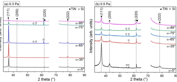
For bothfilm series, the XRD patterns reported inFig. 7show the presence of relatively sharp diffraction lines corresponding to those ex-pected for the cubic (Na-Cl type) structure of TiN. Several reflections, corresponding to (111), (200), (220) and (222) planes, are identified
Fig. 7. XRD patterns of TiNfilms deposited on Si at various tilt angles α and two different working pressures (a) 0.3 Pa and (b) 0.5 Pa. Parasitic reflections from the Si substrate are marked with empty squares.
Fig. 8. Cross-sectional views (in the yz plane) of the computed TiN growth morphology at different Ar pressures and substrate tilt anglesα. For each pressure, results of Simul3D are shown on the left, while those obtained by MODENA are displayed on the right.
at 2θ = 36.8°, 42.5°, 61.8 and 78.3°, respectively, attesting of the forma-tion of polycrystallinefilms. However, compared to reference powder diffraction data (ICDD card n°38-1420), the relative intensity of the 111 diffraction line is much higher, suggesting that TiNfilms develop a [111] preferred orientation. XRD polefigure measurements (not shown here) confirm that the texture is along the [111] direction, but depending on the substrate tilt angleα, they exhibit either a fiber or a biaxial texture [36]. The biaxial texture, found for the TiNfilms series at 0.3 Pa andα ≥ 65°, is in line with the SEM observations ofFig. 5b. The correlation between texture evolution and substrate/column tilt an-gles will be the focus of another work.
Comparing the intensity and width of the XRD lines between both films series, it can be concluded that increasing the working pressure to 0.5 Pa deteriorates the crystalline quality of thefilms. The larger width is contributed to reduction in grain size and/or increase in microstrain. The higher fraction of oxygen uptake found in thesefilms could also explain the lower diffracted intensity. Finally, no significant shift in the diffraction peak position was observed with varyingα for both films series, suggesting minimal change in the residual stress withα. 3.2.2. Computational results
The cross-section views of the TiN thinfilm morphologies computed at 0.3 and 0.5 Pa, but also at thefictitious 0.0 Pa, are shown inFig. 8using the angular distributions ofFig. 2. For the MODENA code, these angular distributions were used for both N and Ti species. The Simul3D and MODENA simulation boxes are respectively 200 px∗ 5 nm and 200 unit cell∗ 0.212 nm, so their lateral size cannot be directly compared. Note that for better visualization of columns, contrast has been enhanced for images obtained by MODENA (original images showing layer density projection can be found in Fig. S2 of Supplementary material).
Both simulations clearly reproduce a columnar growth, in fairly good agreement with the SEM observations. The nature of the arriving spe-cies (individual Ti and N particles in MODENA code and TiN building blocks in Simul3D code) does not seem to significantly alter the results. For the three sets of pressure, there is an increase of the column tilt angleβ with increasing substrate tilt angle α. At fixed α, the columns appear less tilted with increasing pressure forα N 35°.
We can also observe at low pressure, i.e., 0.0 Pa and 0.3 Pa, that the columns within thefilm are qualitatively larger, better defined and the inter-columnar space increases whenα increases. This trend is in line with experimentalfindings at 0.3 Pa (seeFig. 5a). Straight columns, extending throughout the entirefilm thickness, and having a relatively constant diameter are visible, except atα = 85° where the TiN columns tend to enlarge with increasingfilm thickness. This last trend, columns enlargement with increasingα, is not observed at 0.5 Pa; moreover, the columns exhibit qualitatively a similar profile from a tilt angle of 35°. Some branching between columns can be observed at this higher pressure.Fig. 8also reveals that the columns diameter and inter-columnar spacing tend to increase with increasing pressure at lowα angle, i.e. at 5° and 35°. At higher angles, i.e. 65°and 85°, an opposite be-havior is observed. Simulated structures also reveal bundling phenome-non of some nano-columns in the transverse direction of the particle flux [29], which is further enhanced at highα angles.
4. Discussion
4.1. Influence of working pressure on column tilt angle
The simulated (β) and experimental (βexp) column tilt angles at two different working pressures (0.3 and 0.5 Pa) are plotted against each other inFig. 9. Both KMC models give, qualitatively, similar trends: i) an increment of the column tilt angleβ with respect to the substrate inclina-tion angle, ii) a saturainclina-tion phenomenon observed at highα values and iii) lowerβ values at higher pressure. Computed values reproduce fairly well the experimental evolution, which attests of the reliability of our KMC models. However, it can be noticed that overall simulatedβ values are
closer to the experimental values at higher working pressure (0.5 Pa). Be-cause in the simulations, diffusion events are close to zero at the growing temperature of 300 K, the obtained TiN morphologies are essentially dictated by atomic shadowing. This suggests that at 0.5 Pa thefinal nano-structures are mostly driven by the geometricalflux distribution, while at 0.3 Pa other phenomena occur and influence the growth. This is certainly due to the change in the crystallographic structure and orientation [52] (Fig. 7), which is not taken into account in the simulations. Another contribution which can explain the higher computedβ values compared toβexpat lower pressure is the influence of the deposited energy. As pro-posed by Alvarez et al. [39], at low pressure, hyperthermal particles will transfer, upon impingement on the surface, part of their kinetic energy and momentum to adatoms, favoring preferential displacement in the forward direction of the vaporflux (biased diffusion). Due to both glanc-ing incidence condition and the appearance of new surfaces (the side of the columns) this additional mechanism affects the otherwise tilted co-lumnar growth, straightening the columns up, and making them cast a larger shadow over the substrate. This mechanism, not yet taken into account in the present simulations, likely explains the overestimation of the column tilt angle at 0.3 Pa compared toβexpand the increase of the columns diameter and inter-columnar space.
Experimentally, an increase of the pressure from 0.3 Pa to 0.5 Pa does not have a significant influence on the βexpvalues. Based on the work of Alvarez et al. on Ti OAD MSfilms, increasing the working pressure from 0.3 to 0.5 Pa corresponds to an increase of the thermalization degreeΞ from 0.7 to 1.2, and should result in columns being less inclined at higher pressure [39]. Dervaux et al. [4] reported a monotonous decrease ofβexp from 52.7° to 13.8° in Ti GLADfilms (α = 85°) with increasing sputtering pressure in the 0.13–1.3 Pa range. Similar trends of decreasing column tilt angle with increasing pressure have been reported for other metallic systems in pure Ar discharge [17,18]. In the case of reactive MS, sputtered metal atoms and nitrogen species may present different angular distribu-tions; especially adsorption of nitrogen can be the result of dissociative adsorption of N2molecule, impingement of N+ions or sputtered N atoms when target is operated under compound mode.
Fig. 10compares the dependences of the computed column tilt angle β of TiN films on substrate tilt angle α (Fig. 10a) and on resulting inci-dence angleθres(Fig. 10b) at different working pressures: 0.0, 0.3 and 0.5 Pa. In the absence of collisions between particles (at 0 Pa), the evolution ofβ follows perfectly the tangent rule at low substrate angle (α ≤ 65°) and the Tait's cosine law at high substrate angle (α N 65°). This behavior is commonly reported in the literature [1,2,14,15]. At higher pressure, a deviation from these trends is observed, and the
Fig. 9. Correlation between simulated (β) and experimental (βexp) column tilt angle at two different working pressures: 0.3 and 0.5 Pa. Filled symbols refer to Simul3D, and empty ones to MODENA.
column tilt angle is found to saturate at highα angles, as mentioned above. However, if we plot the computedβ data versus θres, as intro-duced inSection 3.1, then an evolution consistent with the two empir-ical laws is recovered. This indicates thatθresis a relevant parameter to describe and predict the columns tilt angle, and points out to the im-portance of accurately determining the local incidence angle of particle flux reaching the substrate. For evaporation, in the absence of gas scat-tering and using small-size vapor sources, the assumptionα = θresis reasonable, which is no longer the case for MS processes, especially when targets with large dimensions are used as sources and are oper-ated at high working pressure.
4.2. Influence of working pressure on morphological evolution of deposited structures
Fig. 11shows the average layer density evolution of the simulated structures with the substrate tilt angle and working pressure. Data ex-tracted from both KMC models display the same trend, even if Simul3D produces in all cases denserfilms (around 10% more) than MODENA. A decrease of the layer density is observed with the increase ofα, the ef-fect being more pronounced at 0.0 Pa, wherefilm densities as low as 30% are obtained forα = 85°. This trend is in good agreement with both experimental and computed data reported for Ti MSfilms grown
at 0.15 Pa [39]. Less variations of the layer density vs.α are found at higher pressures, the lowest values being in the 60–80% range, again in agreement with the data of ref. [39]. This is a direct consequence of the less directional particleflux (seeFig. 2). However, a cross-over phe-nomenon is observed as a function of substrate tilt angle: at low angles (α b 35°), the films at 0.3 Pa are denser than the ones at 0.5 Pa, while at high angles (α N 65°), the opposite situation holds. Such crossover was also reflected in the resistivity evolution with α (seeFig. 6b). Interest-ingly, it can be noticed that the crossover occurs for the maximum value of the resulting incidence angleθres(seeTable 1) meaning there is a critical angle in the interval region 35°b α b 65°, as also revealed for other physical features of OAD metallicfilms [16]. This crossover could be related to the bundling of nano-columns [29], which is en-hanced at higherα angles due to increased shadow length but also de-pends on the surface trapping probability (a higher trapping efficiency being favored at higher pressure). The association of columns in the di-rection transverse to the incomingflux leads to the formation of inter-columnar voids. The larger decrease of thefilm density at 0.3 Pa is likely
Fig. 11. Evolution of the simulated average layer density of TiNfilms with substrate tilt angleα and working pressure. Filled symbols refer to Simul3D, and empty ones to MODENA.
Fig. 12. Evolution of the rms-roughness of TiNfilms with substrate tilt angle α and working pressure. Filled symbols refer to Simul3D, empty ones to MODENA, and the stars refer to experimental data.
Fig. 10. a) Dependence of the computed column tilt angleβ of TiN films a) on substrate tilt angleα and b) resultant incidence angle θresat different working pressures: 0.0, 0.3 and 0.5 Pa. Filled symbols refer to Simul3D, and empty ones to MODENA. The cosine (dotted line) and tangent (dashed line) law-dependences are also indicated.
attributed to the larger inter-columnar spacing (seeFig. 8) associated with higher column tilt anglesβ (seeFig. 10a) and wider coalescing do-mains along the transverse direction. This is supported by the sharper evolution of the resistivity and oxygen content forα N 65° (seeFig. 6). At low substrate angle, alteration of thefilm density is dominated by intra-column vacancies, which in the absence of atom diffusion at 300 K, are formed by shadowing effect.
Fig. 12plots the simulated and experimental surface rms-roughness for the two working pressures investigated as a function of substrate tilt angle. The simulated roughness is calculated in pxs and then converted in nanometers with the corresponding resolution: 4 nm/px for Simul3D and 0.212 nm/px for MODENA. Experimentally and numerically, the roughness always increases with the substrate tilt angle. Again, a cross-over phenomenon between the 0.3 and 0.5 Pa series is observed in the simulations with increasingα. Experimentally, such crossover is not ob-served, but there is evidence of a stronger roughness increment with substrate tilt angle at 0.3 Pa compared to the values obtained at 0.5 Pa. 5. Conclusions
In this study we have investigated the microstructures of TiN thin films deposited by reactive magnetron sputtering at various oblique inci-dence angles. The effect of the discharge pressure on the column forma-tion, their inclination with respect to the substrate normal and their surface topography were systematically analyzed and compared to nu-merical KMC simulations on a 3D rigid lattice and using two different bal-listic models. Increasing the substrate tilt angleα resulted to an increase in the surface roughness and TiN columns tilt angleβ. The in-plane ar-rangement of the columns was affected by the angular distribution of the particleflux, resulting in less tilted TiN columns at higher pressure and to a saturation phenomenon at substrate tilt anglesα ≥ 65°.
The increase of the electrical resistivity as a function of the substrate angleα was attributed to the higher post-growth oxidation of TiN films due to increasing inter-columnarfilm porosity at high α angles, this effect being more pronounced at lower pressure. A good agreement between experimentalfindings and KMC modeling of the TiN film growth by Simul3D and MODENA codes was achieved. Atomistic simulations also revealed crossover phenomena between the 0.3 and 0.5 Pa series from the evolution of the layer density and surface roughness versusα angle. This opens route tofinely tune the physical attributes of nanostructures produced by GLAD techniques by optimization of the working pressure. Data availability
The raw/processed data required to reproduce thesefindings cannot be shared at this time as the data also forms part of an ongoing study. Acknowledgements
This work has been performed within the M.ERA-NET project MC2 “Multi-scale Computational-driven design of novel hard nanostructured Coatings” and funded by the French ANR program (Project No. ANR-13-MERA-0002-02). BB acknowledges thefinancial support from the Algerian Ministry of Higher Education and Scientific Research through the grant n°173 of the PNE 2016-17 program.
Appendix A. Supplementary data
Supplementary data to this article can be found online athttps://doi. org/10.1016/j.matdes.2018.09.023.
References
[1] M.M. Hawkeye, M.J. Brett, Glancing angle deposition: fabrication, properties, and applications of micro- and nanostructured thinfilms, J. Vac. Sci. Technol. A 25 (2007) 1317–1335,https://doi.org/10.1116/1.2764082.
[2] A. Barranco, A. Borras, A.R. Gonzalez-Elipe, A. Palmero, Perspectives on oblique angle deposition of thinfilms: from fundamentals to devices, Prog. Mater. Sci. 76 (2016) 59–153,https://doi.org/10.1016/j.pmatsci.2015.06.003.
[3] D.A. Antartis, R.N. Mott, I. Chasiotis, Silicon nanosprings fabricated by glancing angle deposition for ultra-compliantfilms and interfaces, Mater. Des. 144 (2018) 182–191,https://doi.org/10.1016/j.matdes.2018.02.017.
[4] J. Dervaux, P.A. Cormier, P. Moskovkin, O. Douheret, S. Konstantinidis, R. Lazzaroni, S. Lucas, R. Snyders, Synthesis of nanostructured Ti thinfilms by combining glancing angle deposition and magnetron sputtering: a joint experimental and modeling study, Thin Solid Films 636 (2017) 644–657,https://doi.org/10.1016/j.tsf.2017.06.006. [5] S. Sadeghi-Khosravieh, K. Robbie, Morphology and crystal texture in tilted columnar micro-structured titanium thinfilm coatings, Thin Solid Films 627 (2017) 69–76,
https://doi.org/10.1016/j.tsf.2017.02.038.
[6] Y.G. Yang, D.D. Hass, H.N.G. Wadley, Porosity control in zig-zag vapor-deposited films, Thin Solid Films 471 (2005) 1–11,https://doi.org/10.1016/j.tsf.2004.02.034. [7] X. Xu, M. Arab Pour Yazdi, J.B. Sanchez, A. Billard, F. Berger, N. Martin, Exploiting the
dodecane and ozone sensing capabilities of nanostructured tungsten oxidefilms, Sensors Actuators B Chem. 266 (2018) 773–783,https://doi.org/10.1016/j.snb.
2018.03.190.
[8] A. Ferreira, J. Borges, C. Lopes, N. Martin, S. Lanceros-Mendez, F. Vaz, Piezoresistive response of nano-architectured TixCuythinfilms for sensor applications, Sensors Ac-tuators A Phys. 247 (2016) 105–114,https://doi.org/10.1016/j.sna.2016.05.033. [9] C. Charles, N. Martin, M. Devel, Optical properties of nanostructured WO3 thinfilms
by GLancing Angle Deposition: comparison between experiment and simulation, Surf. Coat. Technol. 276 (2015) 136–140,https://doi.org/10.1016/j.surfcoat.2015.
06.051.
[10] A.G. Dirks, H.J. Leamy, Columnar microstructure in vapor-deposited thinfilms, Thin Solid Films 47 (1977) 219–233,https://doi.org/10.1016/0040-6090(77)90037-2. [11] R. Alvarez, C. Lopez-Santos, J. Parra-Barranco, V. Rico, A. Barranco, J. Cotrino, A.R.
Gonzalez-Elipe, A. Palmero, Nanocolumnar growth of thinfilms deposited at oblique angles: beyond the tangent rule, J. Vac. Sci. Technol., B 32 (2014), 041802.
https://doi.org/10.1116/1.4882877.
[12] B. Tanto, G. Ten Eyck, T.M. Lu, A model for column angle evolution during oblique angle deposition, J. Appl. Phys. 108 (2010), 026107.https://doi.org/10.1063/1.
3465296.
[13] H. Zhu, W. Cao, G.K. Larsen, R. Toole, Y. Zhao, Tilting angle of nanocolumnarfilms fabricated by oblique angle deposition, J. Vac. Sci. Technol. B 30 (2012), 030606.
https://doi.org/10.1116/1.4710999.
[14]J.M. Nieuwenhuizen, H.B. Haanstra, Microfractography of thinfilms, Philips Tech.
Rev. 27 (1966) 87–91.
[15] R. Tait, T. Smy, M. Brett, Modeling and characterization of columnar growth in evaporated-films, Thin Solid Films 226 (1993) 196–201,https://doi.org/10.1016/
0040-6090(93)90378-3.
[16] A. Siad, A. Besnard, C. Nouveau, P. Jacquet, Critical angles in DC magnetron glad thin films, Vacuum 131 (2016) 305–311,https://doi.org/10.1016/j.vacuum.2016.07.012. [17] J.M. García-Martín, R. Alvarez, P. Romero-Gómez, A. Cebollada, A. Palmero, Tilt angle control of nanocolumns grown by glancing angle sputtering at variable argon pres-sures, Appl. Phys. Lett. 97 (2010), 173103.https://doi.org/10.1063/1.3506502. [18] P. Pedrosa, A. Ferreira, J.M. Cote, N. Martin, M.A.P. Yazdi, A. Billard, S.
Lanceros-Mendez, F. Vaz, Influence of the sputtering pressure on the morphological features and electrical resistivity anisotropy of nanostructured titaniumfilms, Appl. Surf. Sci. 420 (2017) 681–690,https://doi.org/10.1016/j.apsusc.2017.05.175.
[19] R. El Beainou, N. Martin, V. Potin, P. Pedrosa, M.A.P. Yazdi, A. Billard, W-Cu sputtered thinfilms grown at oblique angles from two sources: pressure and shielding effects, Surf. Coat. Technol. 343 (2018) 153–159,https://doi.org/10.1016/j.surfcoat.2017.09.
062.
[20] P. Stempflé, A. Besnard, N. Martin, A. Domatti, J. Takadoum, Accurate control of fric-tion with nanosculptured thin coatings: applicafric-tion to gripping in microscale as-sembly, Tribol. Int. 59 (2013) 67–78,https://doi.org/10.1016/j.triboint.2012.05.026. [21] A. Singh, A. Sharma, M. Tomar, V. Gupta, Tunable nanostructured columnar growth of SnO2for efficient detection of CO gas, Nanotechnology 29 (2018), 065502.
https://doi.org/10.1088/1361-6528/aa9bc0.
[22] J.Q. Xi, M.F. Schubert, J.K. Kim, E.F. Schubert, M. Chen, S.Y. Lin, W. Liu, J.A. Smart, Op-tical thin-film materials with low refractive index for broadband elimination of Fres-nel reflection, Nat. Photonics 1 (2007) 176–179,https://doi.org/10.1038/nphoton.
2007.26.
[23] J. Parra-Barranco, M. Oliva-Ramirez, L. Gonzalez-Garcia, M. Alcaire, M. Macias-Montero, A. Borras, F. Frutos, A.R. Gonzalez-Elipe, A. Barranco, Bending induced self-organized switchable gratings on polymeric substrates, ACS Appl. Mater. Inter-faces 6 (2014) 11924–11931,https://doi.org/10.1021/am5037687.
[24] P.W. Chi, C.W. Su, D.H. Wei, Control of hydrophobic surface and wetting states in ultra-flat ZnO films by GLAD method, Appl. Surf. Sci. 404 (2017) 380–387,https://
doi.org/10.1016/j.apsusc.2017.01.266.
[25] U. Allenstein, E.I. Wisotzki, C. Gräfe, J.H. Clement, Y. Liu, J. Schroers, S. G. Mayr, Binary Fe-Pd submicron structures fabricated through glancing angle deposition (GLAD) for bioapplications, Mater. Des. 131 (2017) 366–374,https://doi.org/10.1016/j.
matdes.2017.06.032.
[26] S. Lucas, P. Moskovkin, Simulation at high temperature of atomic deposition, islands coalescence, Ostwald and inverse Ostwald ripening with a general simple kinetic Monte Carlo code, Thin Solid Films 518 (2010) 5355–5361,https://doi.org/10.
1016/j.tsf.2010.04.064.
[27] V. Godinho, P. Moskovkin, R. Álvarez, J. Caballero-Hernández, R. Schierholz, B. Bera, J. Demarche, A. Palmero, A. Fernández, S. Lucas, On the formation of the porous struc-ture in nanostrucstruc-tured a-Si coatings deposited by dc magnetron sputtering at oblique angles, Nanotechnology 25 (2014), 355705.
[28] R. Alvarez, L. González-García, P. Romero-Gómez, V. Rico, J. Cotrino, A.R. Gonzlez-Elipe, A. Palmero, Theoretical and experimental characterization of TiO2thinfilms deposited at oblique angles, J. Phys. D. Appl. Phys. 44 (2011), 385302.https://doi.
org/10.1088/0022-3727/44/38/385302.
[29] C. Lopez-Santos, R. Alvarez, A. Garcia-Valenzuela, V. Rico, M. Loeffler, A.R. Gonzalez-Elipe, A. Palmero, Nanocolumnar association and domain formation in porous thin films grown by evaporation at oblique angles, Nanotechnology 27 (2016), 395702.
https://doi.org/10.1088/0957-4484/27/39/395702.
[30] J.E. Sundgren, Structure and properties of TiN coatings, Thin Solid Films 128 (1985)
21–44.
[31] A.E. Kaloyeros, E. Eisenbraun, Ultrathin diffusion barriers/liners for gigascale copper
metallization, Annu. Rev. Mater. Sci. 30 (2000) 363–385.
[32] B. Shin, Y. Zhu, N.A. Bojarczuk, S. Jay Chey, S. Guha, Control of an interfacial MoSe2 layer in Cu2ZnSnSe4thinfilm solar cells: 8.9% power conversion efficiency with a TiN diffusion barrier, Appl. Phys. Lett. 101 (2012), 053903.https://doi.org/10.
1063/1.4740276.
[33] P. Patsalas, N. Kalfagiannis, S. Kassavetis, Optical properties and plasmonic perfor-mance of titanium nitride, Materials 8 (2015) 3128–3154,https://doi.org/10.3390/
ma8063128.
[34] P. Patsalas, N. Kalfagiannis, S. Kassavetis, G. Abadias, D.V. Bellas, C. Lekka, E. Lidorikis, Conductive nitrides: growth principles, optical and electronic properties, and their perspectives in photonics and plasmonics, Mater. Sci. Eng. R. Rep. 123 (2018) 1–55,https://doi.org/10.1016/j.mser.2017.11.001.
[35] S. Venkataramanababu, G. Nair, P. Deshpande, M.A. Jithin, S. Mohan, A. Ghosh,
Chiro-plasmonic refractory metamaterial with Titanium Nitride (TiN) core-shell nanohelices, Nanotechnology 29 (2018) 255203.
[36] S. Mahieu, P. Ghekiere, D. Depla, R. De Gryse, Biaxial alignment in sputter deposited thinfilms, Thin Solid Films 515 (2006) 1229–1249,https://doi.org/10.1016/j.tsf.
2006.06.027.
[37] Z. Xie, X. Liu, W. Wang, C. Liu, Z. Li, Z. Zhang, Fabrication of TiN nanostructure as a hydrogen peroxide sensor by oblique angle deposition, Nanoscale Res. Lett. 9 (2014) 105,https://doi.org/10.1186/1556-276X-9-105.
[38] Z. Xie, Y.B. Zhang, X.X. Liu, W.P. Wang, P. Zhan, Z.C. Li, Z.J. Zhang, Visible light photoelectrochemical properties of N-doped TiO2nanorod arrays from TiN, J. Nanomater. 2013 (2013), 930950.https://doi.org/10.1155/2013/930950. [39] R. Alvarez, J.M. Garcia-Martin, A. Garcia-Valenzuela, M. Macias-Montero, F.J. Ferrer, J.
Santiso, V. Rico, J. Cotrino, A.R. Gonzalez-Elipe, A. Palmero, Nanostructured Ti thin films by magnetron sputtering at oblique angles, J. Phys. D.: Appl. Phys. 49 (2016), 045303.https://doi.org/10.1088/0022-3727/49/4/045303.
[40] V. Elofsson, D. Magnfält, M. Samuelsson, K. Sarakinos, Tilt of the columnar micro-structure in off-normally deposited thinfilms using highly ionized vapor fluxes, J. Appl. Phys. 113 (2013), 174906.https://doi.org/10.1063/1.4804066.
[41] G. Greczynski, J. Jensen, L. Hultman, Mitigating the geometrical limitations of con-ventional sputtering by controlling the ion-to-neutral ratio during high power pulsed magnetron sputtering, Thin Solid Films 519 (2011) 6354–6361,https://doi.
org/10.1016/j.tsf.2011.04.031.
[42] G. Abadias, L.E. Koutsokeras, S.N. Dub, G.N. Tolmachova, A. Debelle, T. Sauvage, P. Villechaise, Reactive magnetron cosputtering of hard and conductive ternary nitride thinfilms: Ti-Zr-N and Ti-Ta-N, J. Vac. Sci. Technol. A 28 (2010) 541–551,https://
doi.org/10.1116/1.3426296.
[43] G. Abadias, I.A. Saladukhin, V.V. Uglov, S.V. Zlotski, D. Eyidi, Thermal stability and ox-idation behavior of quaternary TiZrAlN magnetron sputtered thinfilms: influence of the pristine microstructure, Surf. Coat. Technol. 237 (2013) 187–195,https://doi.
org/10.1016/j.surfcoat.2013.07.055.
[44] K. Van Aeken, S. Mahieu, D. Depla, The metalflux from a rotating cylindrical
magne-tron: a Monte Carlo simulation, J. Phys. D.: Appl. Phys. 41 (2008) 205307.
[45] J.F. Ziegler, J.P. Biersack, U. Littmark, The Stopping and Range of Ions in Matter,
Pergamon Press, New York, 1985.
[46] G. Abadias, L.E. Koutsokeras, A. Siozios, P. Patsalas, Stress, phase stability and oxida-tion resistance of ternary Ti-Me-N (Me = Zr, Ta) hard coatings, Thin Solid Films 538 (2013) 56–70,https://doi.org/10.1016/j.tsf.2012.10.119.
[47]H. Windischmann, Intrinsic stress in sputter-deposited thinfilms, Crit. Rev. Solid
State Mater. Sci. 17 (1992) 547–596.
[48] A. Besnard, N. Martin, L. Carpentier, Three-dimensional growth simulation: a study of substrate orientedfilms, IOP Conf. Ser. Mater. Sci. Eng. 12 (2010), 012011.https://
doi.org/10.1088/1757-899X/12/1/012011.
[49] F. Nita, C. Mastail, G. Abadias, Three-dimensional kinetic Monte Carlo simulations of cubic transition metal nitride thinfilm growth, Phys. Rev. B 93 (2016), 064107.
https://doi.org/10.1103/PhysRevB.93.064107.
[50] I. Petrov, P.B. Barna, L. Hultman, J.E. Greene, Microstructural evolution duringfilm growth, J. Vac. Sci. Technol. A 21 (2003) S117–S128,https://doi.org/10.1116/1.
1601610.
[51] S. Mahieu, D. Depla, Reactive sputter deposition of TiN layers: modelling the growth by characterization of particlefluxes towards the substrate, J. Phys. D.: Appl. Phys. 42 (2009), 053002.https://doi.org/10.1088/0022-3727/42/5/053002.
[52] D. Depla, A. Besnard, J. Lamas, The influence of the pressure on the microstructure of yttria-stabilized zirconia thinfilms deposited by dual magnetron sputtering, Vac-uum 125 (2016) 118–122,https://doi.org/10.1016/j.vacuum.2015.12.013.