www.advmat.de
Understanding the Structure and Properties of
Sesqui-Chalcogenides (i.e., V
2
VI
3
or Pn
2
Ch
3
(Pn = Pnictogen,
Ch = Chalcogen) Compounds) from a Bonding Perspective
Yudong Cheng, Oana Cojocaru-Mirédin, Jens Keutgen, Yuan Yu, Michael Küpers,
Mathias Schumacher, Pavlo Golub, Jean-Yves Raty, Richard Dronskowski,
and Matthias Wuttig*
DOI: 10.1002/adma.201904316
A number of sesqui-chalcogenides show remarkable properties, which make them attractive for applications as thermo-electrics, topological insulators, and phase-change materials. To see if these properties can be related to a special bonding mechanism, seven sesqui-chalcogenides (Bi2Te3, Bi2Se3, Bi2S3, Sb2Te3, Sb2Se3, Sb2S3, and β-As2Te3) and GaSe are
investigated. Atom probe tomography studies reveal that four of the seven sesqui-chalcogenides (Bi2Te3, Bi2Se3, Sb2Te3,
and β-As2Te3) show an unconventional bond-breaking mechanism. The same four compounds evidence a remarkable
property portfolio in density functional theory calculations including large Born effective charges, high optical dielec-tric constants, low Debye temperatures and an almost metal-like elecdielec-trical conductivity. These results are indicative for unconventional bonding leading to physical properties distinctively different from those caused by covalent, metallic, or ionic bonding. The experiments reveal that this bonding mechanism prevails in four sesqui-chalcogenides, characterized by rather short interlayer distances at the van der Waals like gaps, suggestive of significant interlayer coupling. These conclusions are further supported by a subsequent quantum-chemistry-based bonding analysis employing charge par-titioning, which reveals that the four sesqui-chalcogenides with unconventional properties are characterized by modest levels of charge transfer and sharing of about one electron between adjacent atoms. Finally, the 3D maps for different properties reveal discernible property trends and enable material design.
Metavalent Bonding
Y. Cheng, Dr. O. Cojocaru-Mirédin, J. Keutgen, Dr. Y. Yu, Prof. M. Wuttig I. Institute of Physics
Physics of Novel Materials RWTH Aachen University 52056 Aachen, Germany
E-mail: [email protected] M. Küpers, Prof. R. Dronskowski
Chair of Solid State and Quantum Chemistry Institute of Inorganic Chemistry
RWTH Aachen University 52056 Aachen, Germany M. Schumacher
Institute for Theoretical Solid State Physics RWTH Aachen University
52056 Aachen, Germany
Dr. P. Golub
Department of Mechanical Engineering National University of Singapore
9 Engineering Drive 1, Singapore 117575, Singapore Dr. J.-Y. Raty
CESAM and Physics of Solids Interfaces and Nanostructures, B5 Université de Liège B4000 Sart-Tilman, Belgium Dr. J.-Y. Raty UGA CEA-LETI MINATEC Campus
17 rue des Martyrs, F38054 Grenoble Cedex 9, France Prof. R. Dronskowski, Prof. M. Wuttig
Jülich-Aachen Research Alliance (JARA FIT and JARA HPC) RWTH Aachen University
52056 Aachen, Germany Prof. R. Dronskowski
Hoffmann Institute of Advanced Materials Shenzhen Polytechnic
7098 Liuxian Blvd, Shenzhen, China Prof. M. Wuttig
JARA-Institute: Energy-Efficient Information Technology (Green IT) Forschungszentrum Jülich GmbH
52428 Jülich, Germany The ORCID identification number(s) for the author(s) of this article
can be found under https://doi.org/10.1002/adma.201904316.
Chalcogenides are attracting considerable attention due to their striking properties. These characteristics enable a wide range of applications ranging from phase-change materials (PCMs)[1–3]
to thermoelectrics[4] and topological insulators[5,6] for the heavier chalcogenides. The remarkable application potential has been attributed to an unconventional property portfolio.[2,7–9]
© 2019 The Authors. Published by WILEY-VCH Verlag GmbH & Co. KGaA, Weinheim. This is an open access article under the terms of the Creative Commons Attribution-NonCommercial License, which permits use, distribution and reproduction in any medium, provided the original work is properly cited and is not used for commercial purposes.
Selenides and tellurides often possess high values of the Born effective charge Z*, indicative for a large chemical bond polariz-ability. They often do not strictly follow the 8−N rule and show large effective coordination numbers (ECoN) such that ordinary two electron–two center covalent bonds utilizing electron pairs between nearest neighbors are unlikely. Furthermore, these materials regularly reveal high values of the optical dielectric con-stant ε∞, a measure of the electronic polarizability at frequencies above the highest phonon modes. Finally, they show large values of the Grüneisen parameter for transverse optical modes γ TO, indicative of a pronounced lattice anharmonicity, which signifi-cantly reduces the thermal conductivity of the lattice.[7,8,10]
For IV–VI or tetrels-chalcogen compounds such as GeTe or SnTe, this property portfolio has recently been attributed to a bonding mechanism tentatively coined “metavalent” bonding (MVB).[7,8] Materials utilizing this type of bonding are character-ized by unusual properties including high values of Z*, ε∞, and γTO, as well as an ECoN, which would come unexpected taking into account the 8−N rule.[7,8] Furthermore, this bonding mech-anism is accompanied by an unusual bond breaking process.[11] Finally, this unconventional bonding could be located in a 2D map, in a region where about one electron is shared between two nearest neighbors, while the electron transfer between two adjacent atoms is rather modest.[7] As such, “metavalent” bonding has been related to properties such as low thermal conductivities which for the IV–VI compounds are favorable, that is, for applications in thermoelectrics.[12,13] Indeed, it could be shown that the breakdown of this bonding mechanism along the pseudo-binary line between GeTe and GeSe is detri-mental for the power factor, a crucial figure of merit for ther-moelectrics.[13] Recently, a detailed study has been performed, which relates MVB to the favorable thermoelectric properties of several chalcogenides. It discusses among other aspects the role of the band anisotropy and its relationship to bonding.[13]
The bonding mechanism prevalent in sesqui-chalcogenides such as Sb2Se3 or Bi2Se3 compounds has attracted much less attention, even though members of this family possess a range of interesting properties and applications, too.[14] As listed in
Table 1, they can be utilized as thermoelectrics,[15] PCMs,[1,16] and topological insulators.[5,6] These compounds are frequently either denoted as V2VI3 compounds, where V and VI present an element of group V or group VI, or alternatively as the Pn2Ch3 family, where Pn represents a pnictogen like As, Sb, or Bi, while Ch stands for a chalcogen such as S, Se, or Te. The similarity in properties between IV–VI compounds and V2VI3 compounds raises the question if they can be attributed to a similar bonding mechanism. While the resemblance of proper-ties would be in favor of such a similarity, differences in struc-ture might indicate otherwise. V2VI3 or Pn2Ch3 systems such as Sb2Te3 have been frequently described as 2D solids, where the large spacing between adjacent Te layers has often been termed as van der Waals gap.[17,18] Across such a gap, only weak van der Waals attraction should prevail, hence effectively decoupling adjacent Sb2Te3 quintuples. Indeed, related chalcogenides such as Bi2Te3 and Bi2Se3 are often listed as 2D materials.[17,18] These 2D materials are currently attracting a great deal of attention, as they promise the realization of new functionalities.[17,19] Yet, the picture of 2D behavior is difficult to combine with the idea of metavalent bonding, a bonding mechanism between electron
delocalization (as in metallic bonding) and electron localization (as in covalent bonding), which leads to significant electronic interactions of intermediate distance. The weak coupling that should exist across van der Waals gaps thus seems incompat-ible with such a bonding mechanism.
Thus, it is fair to say that the bonding mechanism in V2VI3 compounds has not yet been determined beyond doubt, in par-ticular because different bonding mechanisms could exist in the same material but spatially separated from each other.[21] Hence, it is highly desirable to study systematic trends for the bonding in the family of V2VI3 compounds, addressing the question if they can be adequately described as 2D solids (which we will refuse in what follows). Furthermore, it needs to be clarified if the remarkable application and property port-folio in certain V2VI3 compounds (Bi2Te3, Bi2Se3, Sb2Te3, and β-As2Te3) can be attributed to a unique bonding mechanism, which differs significantly from the well-established mecha-nisms of ionic, metallic, and covalent bonding.
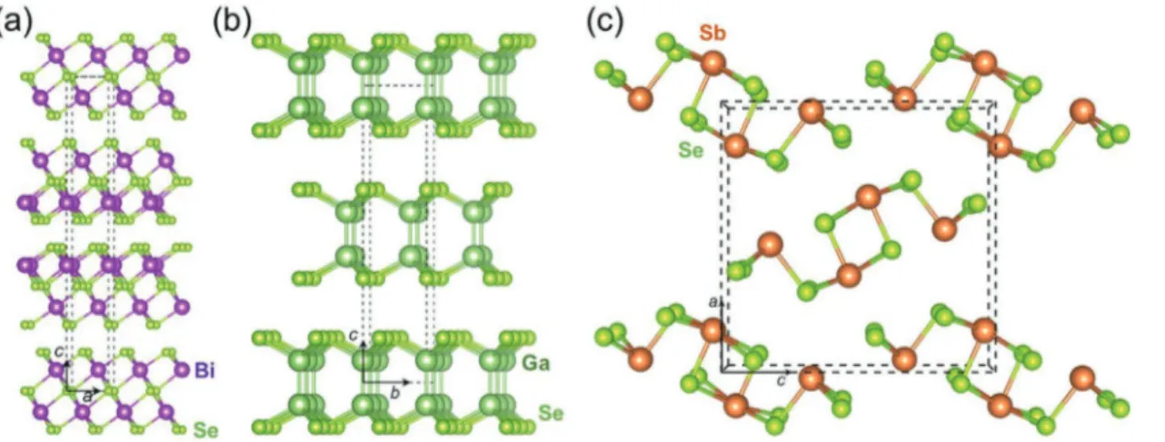
To unravel systematic trends for the properties and, pos-sibly, chemical bonding in V2VI3 compounds, we study Bi2Te3, Bi2Se3, Bi2S3, Sb2Te3, Sb2Se3, and Sb2S3 as well as β-As2Te3, and compare the properties and characteristics with one rep-resentative 2D material, that is, GaSe. The crystal structures of these materials are shown in Figure 1. Four of these sesqui-chalcogenides possess layered structures (Bi2Te3, Bi2Se3, Sb2Te3, and β-As2Te3), composed of stacks of quintuplets (Figure 1a). These quintuplets are spatially separated by gaps, which are frequently called van der Waals gaps, for simple but not neces-sarily justified reasons. Similarly, GaSe, a typical 2D material, also has a layered structure, where quadruplets are separated by van der Waals gaps (see Figure 1b). Finally, as shown in Figure 1c, Sb2Se3 reveals an orthorhombic structure, different from the other materials studied here. Note that Bi2Te3 and Sb2Te3 have the same structure as Bi2Se3, while Bi2S3 and Sb2S3 adopt the same structure as Sb2Se3. In the following, we will Table 1. Structures and some applications of V2VI3 compounds. The
figure-of-merit zT values are extracted from ref. [20]; all topological insu-lator properties are taken from ref. [5]; and PCM properties are taken from refs. [1,16].
Crystal structure Thermoelectricity (figure of merit @300 K) Topological insulator Phase-change material Bi2Te3 Rhombohedral(R3m) Yes (0.57) Yes Yes
Bi2Se3 Rhombohedral(R3m) Yes (0.52) Yes Yes
Bi2S3 Orthorhombic (Pnma) No (0.009) No No
Sb2Te3 Rhombohedral(R3m) Yes (0.3) Yes Yes
Sb2Se3 Orthorhombic (Pnma) No (unmeasurable) No No Sb2S3 Orthorhombic (Pnma) No (unmeasurable) No No β- As2Te3 Rhombohedral(R3m) Yes (0.2‖, 0.38⊥)a) – – a)0.2
‖ and 0.38⊥ are figure-of-merit zT values parallel and perpendicular to hot
employ different techniques to characterize and compare the bonding in these compounds.
We start by employing atom probe tomography (APT), where laser-assisted field evaporation is utilized to break bonds.[22,23] During a laser-assisted APT measurement, a DC voltage of 3–8 kV is applied to a needle-shaped specimen, which is exposed to laser pulses of 10–30 pJ and a fixed pulse length of 10 ps. Upon the combined effect of the applied field and the laser pulse, the surface atoms at the tip are desorbed and ionized.[22] Usually, detection rates (percentage of successful laser pulses) are employed, where only a small fraction of all pulses leads to the rupture of bonds at the apex of specimen and hence to the detection of ions on the position-sensitive detector, contrary to “nulls” where no bond rupture is detected. In our case, detec-tion rates between 0.5 and 2.5% have been chosen. Generally, during an APT measurement, a successful laser pulse, that is, one that manages to dislodge ions from the tip, most probably leads only to one single ion on the detector (single event), while only a small fraction of laser pulses leads to more than one ion on the detector called “multiple events.” Yet, a small but not-zero probability of multiple events is always observed during APT
measurements.[24,25] Surprisingly, recently an unconventional and characteristic pattern of bond rupture has been found for a number of chalcogenides, where a successful laser pulse has a high probability of dislodging not one but several ions, a col-lective effect.[11] We have utilized the same technique to study the bond rupture in sesqui-chalcogenides. Subsequently, we will relate the bond breaking observed to the characteristic properties of the material.
The laser–matter interaction in laser-assisted APT measure-ments is highly dependent on both the sample’s bandgap and the photon energy of the laser.[22,26,27] In general, materials with a bandgap larger than the laser photon energy show a more complex evaporation behavior.[27,28] Yet, the materials studied here all possess bandgaps lower than the laser photon energy as listed in Table S1 (Supporting Information). Hence, one would expect a similar bond breaking behavior for the com-pounds studied if they would all employ a similar bonding mechanism. Instead, striking differences are observed from the data depicted in Figure 2.
As shown in Figure 2a, for Sb2Se3 and GaSe we mainly observe single events, and their probabilities are 95.5% and Figure 1. a–c) Structural models of Bi2Se3 (a), GaSe (b), and Sb2Se3 (c).
Figure 2. a) Distribution of the size of multiple events for the three exemplary compounds Bi2Se3, Sb2Se3, and GaSe. The x-axis denotes the number
of ions (“size”) detected during one successful laser pulse. Therefore, “1” represents single events, while all others are multiple events. For Bi2Se3, a
high probability of multiple events is detected, which demonstrates that the bond breaking in Bi2Se3 differs significantly from bond rupture in Sb2Se3
and GaSe. b) Probabilities of the formation of multiple events for the compounds studied here. Only Bi2Te3, Bi2Se3, Sb2Te3, and β-As2Te3 show a high
probability to form multiple events, while Bi2S3, Sb2Se3, Sb2S3, and GaSe are characterized by an ordinary bond rupture, that is, a low probability of
multiple events. The same experimental conditions (laser pulse energy of 10 pJ, base temperature of 40 K, and detection rate of 1.0%) were used for all measurements depicted here.
80.9%, respectively. In the rare cases that a multiple event is observed for GaSe and Sb2Se3, it most probably only contains two ions. On the contrary, the “collectiveness” (i.e., both the pro-portion and “size” of multiple events) is much larger in Bi2Se3, where even eightfold multiple events are clearly visible. There-fore, the observed high probability of multiple events (69.4%) as well as the large “size” of multiple events (up to eight) dis-tinguishes Bi2Se3 from Sb2Se3 and GaSe. The drastic contrast is also displayed for other compounds studied. As shown in Figure 2b, for Bi2S3, Sb2Se3, and Sb2S3 we mainly observe single events, and the probabilities of multiple events range from 5.6% to 20.7%. The probability of multiple events for GaSe is even lower (4.6%). However, for Bi2Se3, Bi2Te3, Sb2Te3, and β-As2Te3, multiple events form the majority, and the probabilities for such events range from 69.4% to 84.3%. The detailed distribu-tions of the “size” of multiple events for other materials can be found in Figure S1a (Supporting Information). Hence, we observe a striking difference in bond breaking between Bi2S3, Sb2Se3, Sb2S3, and GaSe on the one hand and Bi2Se3, Bi2Te3, Sb2Te3, and β-As2Te3 on the other hand. This is rather sur-prising since Bi2Se3 and Sb2Se3, for example, are isoelectronic. Furthermore, Bi and Sb are chemically very similar; hence, one would have expected that the bond breaking of their selenides also closely resembles each other. Yet, regarding their bond breaking, they fall into two different categories. As discussed in detail in the Supporting Information, these differences are independent of detection rate and laser pulse energy. The large difference in the probability of multiple events between Bi2Te3, Bi2Se3, Sb2Te3, and β-As2Te3 as compared with Bi2S3, Sb2Se3, and Sb2S3 (and GaSe) hence points to intrinsic differences in bond rupture for these two classes of sesqui-chalcogenides.
Multiple events in APT measurements have already been seen previously by many researchers.[24,25] The generation of multiple events is usually attributed to two mechanisms: (1) correlated evaporation which refers to the subsequent evapora-tion of nearest neighbors at kink posievapora-tions; and (2) field dis-sociation describing the decomposition of a larger molecular ion into two or more smaller ions.[24,25] First, the multiple events produced by correlated evaporation usually have much lower probability (not higher than 10–20%), that is,
signifi-cantly lower than our case. Second, the absence of “dissociation tracks” in the correlation histogram in Figure S2 (Supporting Information) excludes field dissociation as the mechanism responsible for the formation of multiple events observed here, as discussed in more detail in the Supporting Information. Hence, the high probability of multiple events in our case is neither caused by ordinary correlative evaporation[24] nor disso-ciation of ions on their path to the detector.[25] Instead, the high probability of multiple events provides ample evidence that the bonding in Bi2Te3, Bi2Se3, Sb2Te3, and β-As2Te3 is incompatible with ordinary covalent bonding alone. Interestingly, the same four compounds show remarkable applications ranging from PCMs to topological insulators and thermoelectrics. This raises the question if the unique set of properties and hence applica-tions can be related to an unconventional bonding mechanism. Therefore, in Table 2 we have compiled data for character-istic material properties including the electrical conductivity σ, the Born effective charge Z*, ECoN, and the optical dielectric constant ε∞. With these properties it is possible to distinguish between the prototypes of metallic, ionic, and covalent bonding. It would be ideal to also include a measure of the softness of the lattice, such as the Grüneisen parameter. Even for complex cases such as Bi2Te3 involving a large unit cell, one may cal-culate energy-resolved mode-specific first-principles Grüneisen parameters from which the macroscopic Grüneisen parameter then results as their arithmetic average, in excellent agreement with experiment.[33] Nonetheless, the computational load is so high that we use here the much cheaper Debye temperature to conveniently characterize the bond stiffness/softness. These parameters provide insights into the characteristic property portfolio of the materials studied.
Inspection of Table 2 reveals a striking trend. The proper-ties of the four materials with unconventional bond breaking (Bi2Te3, Bi2Se3, Sb2Te3, and β-As2Te3) differ significantly from the other four chalcogenides, where the bond breaking observed behaves normally (Bi2S3, Sb2Se3, Sb2S3, and GaSe). This is most obvious for the electrical conductivity. It shows a sharp increase of more than nine orders of magnitude moving from Bi2S3 to Bi2Se3 and from Sb2Se3 to Sb2Te3. Clearly, the electrical conductivity may be regarded as a measure of electron Table 2. Physical properties of all compounds studied. The average Born effective charge Z*avg, the effective coordination number (ECoN), the
bandgap (Eg), and the optical dielectric constant (ε∞) are determined by our DFT calculations, while additional data such as ε‖ and ε⊥, the Debye
temperature θD, and the electrical conductivity σ come from the literature.
σa) [S cm−1] Log σ Z*
avg ECoN Eg [eV] ε∞ θDb) [K] ε‖, ε⊥c)
Bi2Te3 6.6 × 10² 2.82 6.19 5.79 0.53 (35.4; 35.4; 25.5) 155 50; 85 Bi2Se3 1.0 × 10³ 3.00 4.98 5.66 0.54 (19.8; 19.8; 12.0) 182 16.5; 29 Bi2S3 2.0 × 10⁻³ −2.69 4.88 4.76 1.36 (14.0; 14.1; 9.7) 284 13; 9 Sb2Te3 2.3 × 10³ 3.36 5.93 5.84 0.29 (39.5; 39.5; 24.7) 162 32.5; 51 Sb2Se3 4.0 × 10⁻⁷ −6.40 4.41 4.17 0.76 (19.1; 18.5; 9.7) 292 15.1; 14.5 Sb2S3 1.0 × 10⁻⁸ −8.00 4.24 3.92 1.28 (14.2; 12.5; 7,34) 364 9.5; 7.2 β-As2Te3 6.5 × 10² 2.81 7.41 5.84 0.26 (65.7; 65.7; 42.6) 148 – GaSe 1.0 × 10⁻⁶ −6.00 1.74 4.00 1.23 (8.2; 8.1; 4.2) 342 7.1; 7.45
a)The electric conductivities are extracted from ref. [29]; b)The Debye temperatures are extracted from refs. [30,31]; c)The experimental optical dielectric constants ε
‖ and ε⊥
delocalization. Hence, it is high in metals and low in undoped materials employing ionic or covalent bonding. Metavalently bonded materials like Bi2Te3, Bi2Se3, Sb2Te3, and β-As2Te3 have intermediate values, significantly higher than those found for undoped ionic or covalently bonded materials. They are related to a remarkably narrow range of electrical conductivities and are close to the Mooij rule for bad metals (see Figure S6, Sup-porting Information), which identifies the critical conductivity where the temperature coefficient of resistivity changes sign in metals to 6 × 10³ S cm−1.[34,35]
Metavalently bonded materials such as PbTe, GeTe, and GeSb2Te4 typically show a characteristic feature, that is, anti-bonding states right at/below the Fermi energy as shown uti-lizing crystal orbital Hamilton population (COHP).[36,37] These antibonding states can be emptied by vacancy formation as demonstrated for a typical PCM GeSb2Te4.[37] Sb2Te3 is also characterized by pronounced antibonding interactions in the highest occupied states close to the Fermi level.[38] To sup-press the antibonding states and stabilize the system, atoms are expelled to form vacancies and the Fermi level is lowered, thereby depopulating those energetically unfavorable states. On the contrary, the COHP of Sb2Se3 shows almost no antibo-nding states close to the Fermi level.[39] Thus, expelling atoms to form vacancies is energetically costlier in covalently bonded Sb2Se3. This can also be supported by two facts: (1) the rather higher formation energy of vacancies in typical covalent mate-rials such as Si, Ge, or GaAs. For example, in Si the forma-tion energy for a vacancy has been calculated to be 3.3 eV;[40] and (2) the increased formation energy of a vacancy along the Bi2Se3-Sb2Se3 pseudo binary line.[41] Hence, the pronounced antibonding states in MVB materials contribute to the high carrier concentration. Besides, the weaker distortion and the delocalized nature of MVB in comparison with the localized covalent bond are also beneficial to the electronic transport, for example, the mobility of Bi2Se3 is higher than that of Sb2Se3.[42] Therefore, it seems adequate to call these compounds incipient metals.[8]
Besides the electrical conductivity, the ECoN[43] is another good measure of the bonding mechanism employed. The ECoN ≈ 4 for tetrahedrally bonded covalent materials (such as III–V or II–VI semiconductors) is what one would expect given the simple 8−N rule. However, the rather high ECoNs for p-bonded Bi2Te3, Bi2Se3, Sb2Te3, and β-As2Te3 are indicative of an elec-tron count incompatible with the 8−N rule. Such high effective coordination numbers are only feasible if the bond order for the nearest neighbors is smaller than 1. This is indicative for a low valence electron count per atomic neighbor and resem-bles metal-like behavior,[35] in line with the high conductivities observed.
Moreover, three further properties are listed in Table 2, that is, the Born effective charge Z*avg, the optical dielectric constant (ε∞), and the Debye temperature (θD). They all probe different aspects of the bonding nature. ε∞ represents the elec-tronic polarizability, while Z* describes the chemical bond polarizability.[8] The Debye temperature θ
D finally is a measure of the softness of the lattice. First-principle data in Table 2 show that the Born effective charges are smaller for Bi2S3, Sb2S3, and Sb2Se3 than for Bi2Te3, Bi2Se3, Sb2Te3, and β-As2Te3, where atypically high values are observed. Similar trends are observed
for ε∞, too. Finally, the lower Debye temperatures observed for Bi2Te3, Bi2Se3, Sb2Te3, and β-As2Te3 are indicative of overall soft bonds in these compounds.
Hence, for the four sesqui-chalcogenides showing an uncon-ventional bond-breaking mechanism, we observe a remark-able property portfolio. The electronic conductivity is almost metallic, while the violation of the 8−N rule leads to a large ECoN. Furthermore, the optical dielectric constant is unusu-ally large and the chemical bond polarizability (Born effective charge) is quite high. Finally, the bond strength is rather weak, in line with the low Debye temperature. All of these properties point to an exceptional phenomenon. We have recently shown for IV–VI chalcogenides such as GeTe or SnTe that these prop-erties are characteristic for an unconventional bonding mecha-nism.[7,8] The results presented here imply that the same type of bonding is not only found in IV–VI compounds but also prevails in V2VI3 systems such as Bi2Te3, Bi2Se3, Sb2Te3, and β-As2Te3, while other V2VI3 compounds such as Bi2S3, Sb2Se3, and Sb2S3 differ.
The observation of bonding dubbed “metavalent” in Bi2Te3, Bi2Se3, Sb2Te3, and β-As2Te3 is puzzling at first sight, since these materials are characterized by a clear gap between adja-cent quintuples, which has been described as a van der Waals gap. Such a gap implies rather weak coupling between adjacent quintuples, solely based on dispersion forces (induced dipoles) as a consequence of Heisenberg’s uncertainty principle in a region of practically zero density. Hence, a systematic analysis of the gap between adjacent quintuples seems to be in place.
As a rule of thumb, a shorter interatomic distance for the same compound typically signals a larger bond strength although deviations exist for both molecules and solids. Hence, rather simple bond length–bond strength concepts are fre-quently utilized to rationalize the structure of molecules and solids.[44] We also follow this train of thought based on bond lengths in Figure 3 to compare the interatomic coupling between two chalcogenide atoms, that is, “TeTe” or “SeSe” which we assume to be van der Waals like to begin with. Theo-retically, the van der Waals bond length is equal to (or longer than) the sum of van der Waals radii of the two constituting atoms. To facilitate the comparison of different chalcogenides, the resulting distance is normalized to the theoretical van der Waals bond length as mentioned above. For the four chalcoge-nides Bi2Te3, Bi2Se3, Sb2Te3, and β-As2Te3, the interatomic dis-tance is significantly shorter (≈10–15%) than expected for a van der Waals bonded system. On the contrary, for the van der Waals bonded system GaSe the distance between adjacent Se atoms across the gap is even slightly larger by 2.9%. Therefore, for the four sesqui-chalcogenides Bi2Te3, Bi2Se3, Sb2Te3, and β-As2Te3, the coupling across the gap is very likely to be stronger than expected for weak van der Waals bonding. If that is true, the reduced interlayer spacing and considerable coupling across the van der Waals like gap suggest an additional energetic contribu-tion besides the weak van der Waals bonding. This argument is further supported by the calculation of the fraction of elec-trons between adjacent chalcogenide layers. While in GaSe only a small fraction of an electron (0.04 e) is shared between adja-cent Se atoms across the gap, the corresponding numbers are much higher for Bi2Te3 (0.272 e), Bi2Se3 (0.132 e), Sb2Te3 (0.244 e), and β-As2Te3 (0.192 e), which identifies a significant charge
density between adjacent layers. The charge shared between adjacent chalcogenide layers provides evidence for significant coupling between these layers. We can hence conclude that the bonding mechanism between two quintuple stacks in layered V2VI3 compounds (Bi2Te3, Bi2Se3, Sb2Te3, and β-As2Te3) is not a pure van der Waals bond but a stronger interatomic inter-action. Together with the unique bond breaking process and anomalously high physical properties observed for these sesqui- chalcogenides, this alludes to an unconventional bonding mechanism in this material class.
We have recently shown that bonding coined “metavalent” in IV–VI compounds is also characterized by a unique range of electrons being shared and transferred between nearest neigh-bors.[7] All IV–VI compounds which showed unusual bond breaking and unconventional properties are characterized by roughly one electron being shared between nearest neighbors and a modest electron transfer.[7] Clearly, this is neither the situ-ation encountered in covalently bonded materials like diamond (roughly two electrons, i.e., one electron pair) nor in metals, where much fewer electrons are available due to the large number of nearest neighbors, or in ionic compounds, where significant charge transfer occurs. This is further evidence that we are dealing with an unconventional bonding mecha-nism. Hence, in the following we will try to determine the number of electrons shared and electrons transferred between
neighboring atoms in the class of V2VI3 compounds. The cal-culation method is similar to ref. [7] but slightly trickier than for the IV–VI compounds discussed there, since now we have two different chalcogen sites, which differ in their number of electrons shared and electrons transferred to the neighboring main-group V atom. In the Supporting Information, we hence list the values for the electrons shared and electrons trans-ferred for all atoms in the unit cell. Subsequently, the average value has been computed, which is plotted in Figure 4. Nev-ertheless, it has to be verified if the behavior of the material can indeed be adequately described by such an average. After all, it is possible that one bond could be covalent, while the other one might be metallic, but the average appears as if the atoms would be metavalently bonded. There is a second sub-tlety, which ought to be addressed. The map depicted in ref. [7] utilizes the total number of electrons transferred as the x-axis. Clearly, this provides the means to differentiate ionic bonding from metallic bonding. However, using the total number of electrons transferred (see Figure S5, Supporting Information) leads to an x-axis value for MgO of 1.70, while NaCl is charac-terized by an electron transfer of 0.87. It hence might appear that MgO is significantly more ionic than NaCl. This is not the case, if the relative electron transfer is considered, which is obtained by dividing the absolute electron transfer by the oxidation state of the corresponding atom. For MgO, we thus obtain a relative electron transfer of 0.85, while NaCl is charac-terized by a relative electron transfer of 0.87. Thus, regarding the relative charge transfer, NaCl and MgO have very similar ionic character, in line with chemical intuition. We can now use this approach to characterize the charge transfer in the class of V2VI3 compounds, where we divide the charge transfer of the group V element by 3, while the charge transfer of the group VI element is divided by two.
The chemical bonding of the materials studied is visualized in a 2D map shown in Figure 4. While material maps have already been presented in the last 50 years for various reasons, the present approach adds something new. First of all, the coordinates of the map are obtained directly from a solution of the Kohn–Sham equation and a density partitioning, not from empirical quantities. Furthermore, the map employs “natural” coordinates to separate bonding mechanisms, since sharing electrons between adjacent atoms and/or transferring elec-trons seem to be the “natural coordinates” to describe bonding. The resulting map distinguishes ionic, covalent, and metallic bonding, which are located in three distinct regions of the map. Ionic bonding (black points) is characterized by significant charge transfer, but only a modest degree of electrons shared between adjacent atoms. On the contrary, covalent bonding is defined by a significant sharing of electrons, distributing close to two electrons between adjacent atoms. Metallic bonding is characterized by small or vanishing electron transfer between adjacent atoms, but also only small degree of electron sharing between adjacent atoms. Van der Waals solids are finally located in the lower left corner, characterized by essentially zero elec-tron sharing. Hence, all four bonding mechanisms are located in clearly separable regions of the map.
Interestingly, there is a gradual transition from covalent to ionic bonding, in line with chemical intuition recognizing that materials like GaN or ZnO are polar semiconductors, that is, Figure 3. Interatomic distance between adjacent chalcogenide atoms
across the van der Waals like gap. To facilitate the comparison of different chalcogenides, the resulting distance is normalized to the theoretical van der Waals bond length by dividing the sum of van der Waals radii of two constituent atoms. The interatomic distances of Bi2Se3 (left) and GaSe
(right) and the theoretical van der Waals bond length are sketched in the lower panel. The light green circles denote the van der Waals radius of Se. Note that the distances are not proportional to the real value in order to stress the difference between these two compounds.
they have both ionic and covalent bonding contributions. One key feature of the present map is that both contributions can now be adequately characterized by the number of electrons shared and electron transferred. The green region in-between denotes all materials which show an unconventional property portfolio including high effective coordination numbers, large Born effective charges, high optical dielectric constants, rather low Debye temperatures, and an almost metal-like electrical conductivity. These materials clearly fall in a distinct region of its own.
We can now draw the points for the seven sesqui-chalcoge-nides we have studied. As one can see in this figure, they fall in two different groups regarding their bond breaking and proper-ties. Hence, also in the map these two pairs of compounds span two separate regions, which do not overlap. Bi2S3, Sb2Se3, and Sb2S3 are all located in the region of covalent bonding. On the contrary, Bi2Te3, Bi2Se3, Sb2Te3, and β-As2Te3 are found in the region characteristic for metavalent bonding. In the very same region, also octahedrally coordinated IV–VI compounds (tetrel-chalcogenides), such as GeTe, SnTe, or PbSe are found, which show the unconventional property portfolio of metavalently bonded materials.[7] This raises the question if there are simi-larities between, for example, GeTe and Sb2Te3. Both material classes show a similar atomic arrangement. Their structures can both be described as a distorted octahedral arrangement. This similarity in atomic arrangement and, at the same time, prop-erties is indicative for a pronounced resemblance in bonding.
The bonding in GeTe has been attributed to a half-filled band of p-electrons, that is, on average three p-electrons per atom.[45] This is due to the fact that there is very little s-p hybridization (or orbital mixing), so that the p-electrons govern bond formation.[31,46] With two p-electrons from Ge and four p-electrons from Te, on average three p-electrons per atom are available. These p-electrons give rise to σ-bonds between adjacent atoms, which lead to the observed octahedral atomic arrangement. The same situation is also encountered in Sb2Te3. Again, per site (if we also include one vacancy per quintuplet), three p-electrons are available. Hence, the corresponding p-band is half-filled. Energy minimization is achieved by formation of σ-bonds in GeTe and Sb2Te3 which causes an octahedral atomic arrangement in both cases. Yet, this electronic configuration is unstable, as can be seen in Figure 5b. The electronic energy can either be reduced by a structural distortion or by charge transfer between adjacent atoms. For simplicity, we consider a 1D chain (“Ι”) in Figure 5a,b, leading to a simple parabolic band structure. This config-uration is unstable against electron transfer (top) or Peierls distortion (1D atomic chain “ΙΙ” and “ΙΙΙ”), leading to the opening of a gap. The stronger the distortion, the larger the bandgap and the resulting decrease of potential energy. This phenomenon and the resulting influence on bonding mechanism are also visible in Figure 4. In this 2D electronic map, all ideal rocksalt-type struc-tures of systems which utilize σ-bonds of p-levels, are located on one line, spanning from AgSbTe2 to PbSe, while all dis-torted octahedrally coordinated structures are characterized by a higher level of electrons shared which eventually undermines the metavalent bonding and finally causes the transition toward covalent bonding.
The calculated density of states of Sb2Te3 and Sb2S3 con-firms this view. Both the valence and the conduction band are dominated by p-levels, even though the distortion is much more pronounced for Sb2S3. The size of the Peierls distor-tion apparently scales with the increase of the number of electrons shared above one. If we ignore electron transfer, the ideal octahedral structure is found for one electron shared between adjacent atoms. This can be seen in Figure 4, where the cubic (undistorted systems) are lying on one line. Bi2Se3 and Sb2Se3 have same level of electron transfer but appar-ently a different count of electrons shared, equivalappar-ently, they differ in the degree of Peierls distortion (see Table S3, Sup-porting Information). In Sb2Te3, Bi2Se3, Bi2Te3, and β-As2Te3, weak Peierls distortions prevail. Hence, about one electron is shared between adjacent atoms. In Sb2S3, on the contrary, a much stronger Peierls distortion occurs, incompatible with metavalent bonding. This is further supported by the large bandgap and the more distorted octahedral motifs of Sb2S3, Sb2Se3, and Bi2S3.
Figure 4. 2D map describing bonding in solids. The map is spanned by the electron transfer
between adjacent atoms and the sharing of electrons between them. Triangles, diamonds, squares, and circles denote tetrahedrally bonded solids, distorted and ideal rocksalt-type (octa-hedrally coordinated) structures, body-centered solids, and close-packed metals, respectively, while filled and open symbols represent thermodynamically stable and metastable phases. Larger symbols denote the seven sesqui-chalcogenides studied here. All ideal rocksalt struc-tures for materials with half-filled p-bands are located on one line, spanning from AgSbTe2 to
PbSe, while all distorted octahedrally coordinated structures are situated above it, characterized by a larger number of electrons shared.
In Figure 6, three physical properties are employed to extend the 2D map to a third dimension. In all three maps, the properties of Bi2Te3, Bi2Se3, Sb2Te3, and β-As2Te3 stand out. Furthermore, the properties of these compounds also differ clearly from the characteristics displayed by the other three sesqui-chalcogenides Bi2S3, Sb2Se3, and Sb2S3. This is most obvious for the electrical conductivity, which increases by nine orders of magnitude upon the transition from the cova-lently bonded sesqui-chalcogenides to the metavacova-lently bonded
sesqui-chalcogenides, but also the optical dielectric constant and the Born effective charge Z* for these compounds pro-trude. The unusual values and the apparent discontinuous transition support the view that an unconventional bonding mechanism prevails in Bi2Te3, Bi2Se3, Sb2Te3, and β-As2Te3.
In summary, the wealth of experimental data together with selected theoretical descriptors suggest a unique bonding mechanism for Bi2Te3, Bi2Se3, Sb2Te3, and β-As2Te3. This con-clusion is derived from several observations. Laser-assisted APT
Figure 6. a–c) The 2D map is extended in the third dimension using three independent properties, that is: a) the Born effective charge Z*, b) the
optical dielectric constant ε∞, and c) the electrical conductivity log σ. Black, red, and blue, respectively, describe materials which utilize predominantly
ionic, covalent, and metallic bonding. Green denotes materials with an unconventional property combination and unusual bond breaking as revealed by APT. The corresponding materials are characterized by anomalously high values of all three indicators (green bars), a property portfolio not revealed by any other bonding mechanism.
Figure 5. a) Octahedral atomic arrangement as observed to first approximation in GeTe and Sb2Te3. This arrangement is a consequence of the σ-bonds
formed between adjacent atoms due to the half-filling of the p-band. Such a configuration is unstable, as shown for the schematic of an undistorted 1D atomic chain. Two options exist to lower the energy: electron transfer and atomic distortions (Peierls distortion). b) Both charge transfer and the Peierls distortion lead to an opening of a gap and hence a decrease in potential energy for the occupied states. c) This view is supported by the calculated density of states for Sb2S3 and Sb2Te3. The degree of Peierls distortion is described by the averaged radii of three short (r1) and three long (r2) bonds,
that is, r2/r1. Note that for Sb2S3 (Sb2Se3 and Bi2S3), there are two different cation positions acting as the center of two different octahedral motifs.
These two octahedral motifs have therefore different level of distortion, as indicated by the different values of r2/r1. For both materials, the valence
shows a highly unconventional mechanism of bond breaking, characterized by high probabilities of multiple events exclu-sively observed for four of the eight chalcogenides studied here, that is, Bi2Te3, Bi2Se3, Sb2Te3, and β-As2Te3. Five property-based indicators derived from our density functional theory calcula-tions and literature values show properties which differ signifi-cantly from those characteristics for materials which employ conventional chemical bonds such as ionic, metallic, and cova-lent bonds. The four compounds which show this unconven-tional property portfolio are characterized by a short distance between adjacent chalcogenide layers which is indicative of more than weak van der Waals bonding. This is in line with the increased concentration of electrons between these layers, which is indicative for a pronounced coupling across this gap. Hence, one should refrain from calling these materials 2D solids and denoting the gap as a van der Waals gap.
Our findings enable a number of far-reaching conclusions. There is a considerable number of materials which employ this unconventional type of bonding. These materials are not very ionic and employ p-electrons to form bonds. These p-electrons are neither fully delocalized like in metals nor fully localized as in covalent bonds. Typically, between two neighboring atoms we only find approximately one single electron. Hence, these mate-rials can be localized in a unique region of the map. This region of the map is not only characterized by a well-defined range of values for the electrons shared and electrons transferred between adjacent atoms but also described by the unique properties found there. Hence, the map can be utilized to design material properties. This is crucial since the materials which encompass the unconventional property portfolio and bond breaking have a number of important applications ranging from thermoelectrics to topological insulators and phase-change materials.
Supporting Information
Supporting Information is available from the Wiley Online Library or from the author.
Acknowledgements
The authors are grateful for the support from the Deutsche Forschungsgemeinschaft (DFG) through SFB 917 “Nanoswitches” and the Excellence Initiative (Distinguished Professorship). Y.C. acknowledges financial support from the China Scholarship Council.
Conflict of Interest
The authors declare no conflict of interest.
Keywords
chemical bonding, laser-assisted field evaporation, materials design, sesqui-chalcogenides
Received: July 6, 2019 Revised: August 2, 2019 Published online:
[1] M. Wuttig, N. Yamada, Nat. Mater. 2007, 6, 824.
[2] D. Lencer, M. Salinga, B. Grabowski, T. Hickel, J. Neugebauer, M. Wuttig, Nat. Mater. 2008, 7, 972.
[3] a) S. Raoux, W. Wełnic, D. Ielmini, Chem. Rev. 2010, 110, 240; b) M. Wuttig, H. Bhaskaran, T. Taubner, Nat. Photonics 2017, 11, 465. [4] a) G. J. Snyder, E. S. Toberer, Nat. Mater. 2008, 7, 105; b) M. Hong,
J. Zou, Z. G. Chen, Adv. Mater. 2019, 31, 1807071; c) G. Tan, L.-D. Zhao, M. G. Kanatzidis, Chem. Rev. 2016, 116, 12123. [5] H. Zhang, C.-X. Liu, X.-L. Qi, X. Dai, Z. Fang, S.-C. Zhang, Nat.
Phys. 2009, 5, 438.
[6] D. Hsieh, Y. Xia, D. Qian, L. Wray, F. Meier, J. Dil, J. Osterwalder, L. Patthey, A. Fedorov, H. Lin, Phys. Rev. Lett. 2009, 103, 146401. [7] J. Y. Raty, M. Schumacher, P. Golub, V. L. Deringer, C. Gatti,
M. Wuttig, Adv. Mater. 2019, 31, 1806280.
[8] M. Wuttig, V. L. Deringer, X. Gonze, C. Bichara, J. Y. Raty, Adv.
Mater. 2018, 30, 1803777.
[9] K. Shportko, S. Kremers, M. Woda, D. Lencer, J. Robertson, M. Wuttig, Nat. Mater. 2008, 7, 653.
[10] S. Lee, K. Esfarjani, T. Luo, J. Zhou, Z. Tian, G. Chen, Nat. Commun.
2014, 5, 3525.
[11] M. Zhu, O. Cojocaru-Mirédin, A. M. Mio, J. Keutgen, M. Küpers, Y. Yu, J. Y. Cho, R. Dronskowski, M. Wuttig, Adv. Mater. 2018, 30, 1706735.
[12] a) J. Li, X. Zhang, Z. Chen, S. Lin, W. Li, J. Shen, I. T. Witting, A. Faghaninia, Y. Chen, A. Jain, Joule 2018, 2, 976; b) K. Biswas, J. He, I. D. Blum, C.-I. Wu, T. P. Hogan, D. N. Seidman, V. P. Dravid, M. G. Kanatzidis, Nature 2012, 489, 414; c) L.-D. Zhao, H. J. Wu, S. Q. Hao, C.-I. Wu, X. Y. Zhou, K. Biswas, J. Q. He, T. P. Hogan, C. Uher, C. Wolverton, Energy Environ. Sci. 2013, 6, 3346; d) Y. Pei, X. Shi, A. LaLonde, H. Wang, L. Chen, G. J. Snyder, Nature 2011,
473, 66.
[13] a) M. Cagnoni, D. Führen, M. Wuttig, Adv. Mater. 2018, 30, 1801787; b) Y. Yu, M. Cagnoni, O. Cojocaru-Mirédin, M. Wuttig,
Adv. Funct. Mater. 2019, 29, 190.
[14] a) E. Rotunno, M. Longo, C. Wiemer, R. Fallica, D. Campi, M. Bernasconi, A. R. Lupini, S. J. Pennycook, L. Lazzarini, Chem.
Mater. 2015, 27, 4368; b) R. Wang, F. R. L. Lange, S. Cecchi,
M. Hanke, M. Wuttig, R. Calarco, Adv. Funct. Mater. 2018, 28, 1705901; c) P. A. Vermeulen, J. Mulder, J. Momand, B. J. Kooi,
Nanoscale 2018, 10, 1474.
[15] a) G. Zheng, X. Su, H. Xie, Y. Shu, T. Liang, X. She, W. Liu, Y. Yan, Q. Zhang, C. Uher, Energy Environ. Sci. 2017, 10, 2638; b) T. Zhu, L. Hu, X. Zhao, J. He, Adv. Sci. 2016, 3, 1600004; c) B. Poudel, Q. Hao, Y. Ma, Y. Lan, A. Minnich, B. Yu, X. Yan, D. Wang, A. Muto, D. Vashaee, Science 2008, 320, 634; d) S. I. Kim, K. H. Lee, H. A. Mun, H. S. Kim, S. W. Hwang, J. W. Roh, D. J. Yang, W. H. Shin, X. S. Li, Y. H. Lee, Science 2015, 348, 109.
[16] a) N. Han, S. I. Kim, J. D. Yang, K. Lee, H. Sohn, H. M. So, C. W. Ahn, K. H. Yoo, Adv. Mater. 2011, 23, 1871; b) N. Yamada,
MRS Bull. 1996, 21, 48.
[17] A. K. Geim, I. V. Grigorieva, Nature 2013, 499, 419. [18] A. Gupta, T. Sakthivel, S. Seal, Prog. Mater. Sci. 2015, 73, 44. [19] a) K. S. Novoselov, A. Mishchenko, A. Carvalho, A. H. C. Neto,
Sci-ence 2016, 353, aac9439; b) Y. Cao, V. Fatemi, S. Fang, K. Watanabe,
T. Taniguchi, E. Kaxiras, P. Jarillo-Herrero, Nature 2018, 556, 43. [20] a) J.-B. Vaney, G. Delaizir, A. Piarristeguy, J. Monnier, E. Alleno,
E. B. Lopes, A. P. Goncalves, A. Pradel, A. Dauscher, C. Candolfi,
APL Mater. 2016, 4, 104901; b) Y. Kawamoto, H. Iwasaki, J. Electron. Mater. 2014, 43, 1475; c) K. Biswas, L. D. Zhao, M. G. Kanatzidis, Adv. Energy Mater. 2012, 2, 634; d) J. Jiang, L. Chen, S. Bai,
Q. Yao, Q. Wang, J. Cryst. Growth 2005, 277, 258; e) I. Yashima, H. Watanave, T. Ogisu, R. Tsukuda, S. Sato, Jpn. J. Appl. Phys. 1998,
37, 2472.
[21] a) S. Liu, J. Wei, F. Gan, Appl. Phys. Lett. 2012, 100, 111903; b) X. P. Wang, N. K. Chen, X. B. Li, Y. Cheng, X. Liu, M. J. Xia,
Z. Song, X. Han, S. Zhang, H. B. Sun, Phys. Chem. Chem.
Phys. 2014, 16, 10810; c) Y. Zheng, M. Xia, Y. Cheng, F. Rao,
K. Ding, W. Liu, Y. Jia, Z. Song, S. Feng, Nano Res. 2016, 9, 3453.
[22] B. Gault, M. P. Moody, J. M. Cairney, S. P. Ringer, Atom Probe
Microscopy, Springer, New York 2012.
[23] B. Gault, F. Vurpillot, A. Vella, M. Gilbert, A. Menand, D. Blavette, B. Deconihout, Rev. Sci. Instrum. 2006, 77, 043705.
[24] F. De Geuser, B. Gault, A. Bostel, F. Vurpillot, Surf. Sci. 2007, 601, 536.
[25] D. W. Saxey, Ultramicroscopy 2011, 111, 473.
[26] B. Mazumder, A. Vella, B. Déconihout, Ultramicroscopy 2011, 111, 571.
[27] T. F. Kelly, A. Vella, J. H. Bunton, J. Houard, E. P. Silaeva, J. Bogdanowicz, W. Vandervorst, Curr. Opin. Solid State Mater. Sci.
2014, 18, 81.
[28] A. Vella, Ultramicroscopy 2013, 132, 5.
[29] a) E. I. Elagina, in Proc. 4th Conf. Semiconducting Materials: Current
Topics in Semiconductor Metallurgy and Physics, Akademiya Nauk
SSSR, Moscow 1961, pp. 153–158; b) J. Horák, Z. Starý, M. Matyáš,
J. Solid State Chem. 1991, 93, 485; c) J. B. Vaney, J. Carreaud,
G. Delaizir, C. Morin, J. Monnier, E. Alleno, A. Piarristeguy, A. Pradel, A. P. Goncalves, E. B. Lopes, J. Electron. Mater. 2016, 45, 1786; d) J. Yanez-Limon, J. González-Hernández, J. Alvarado-Gil, I. Delgadillo, H. Vargas, Phys. Rev. B 1995, 52, 16321; e) B. Roy, B. Chakraborty, R. Bhattacharya, A. Dutta, Solid State Commun.
1978, 25, 937; f) J. F. Sánchez-Royo, A. Segura, A. Chevy, L. Roa, J. Appl. Phys. 1996, 79, 204; g) H. T. Shaban, M. M. Nassary,
M. S. El-Sadek, Phys. B 2008, 403, 1655.
[30] a) X. Yang, Z. Zhou, Y. Wang, R. Jiang, W. Zheng, C. Q. Sun,
J. Appl. Phys. 2012, 112, 083508; b) S. Jandl, J. Brebner, B. Powell, Phys. Rev. B 1976, 13, 686; c) Z. Liu, Y. Pei, H. Geng, J. Zhou,
X. Meng, W. Cai, W. Liu, J. Sui, Nano Energy 2015, 13, 554; d) E. S. Toberer, A. Zevalkink, G. J. Snyder, J. Mater. Chem. 2011, 21, 15843.
[31] a) J.-B. Vaney, J.-C. Crivello, C. Morin, G. Delaizir, J. Carreaud, A. Piarristeguy, J. Monnier, E. Alleno, A. Pradel, E. B. Lopes, RSC
Adv. 2016, 6, 52048; b) H. Koc, A. M. Mamedov, E. Deligoz,
H. Ozisik, Solid State Sci. 2012, 14, 1211.
[32] a) O. Madelung, Semiconductors: Data Handbook, Springer Sci-ence & Business Media, Berlin 2012; b) P. Leung, G. Andermann, W. G. Spitzer, C. Mead, J. Phys. Chem. Solids 1966, 27, 849. [33] A. F. Zurhelle, V. L. Deringer, R. P. Stoffel, R. Dronskowski, J. Phys:
Condens. Mater. 2016, 28, 115401.
[34] J. H. Mooij, Phys. Status Solidi A 1973, 17, 521.
[35] T. Siegrist, P. Jost, H. Volker, M. Woda, P. Merkelbach, C. Schlockermann, M. Wuttig, Nat. Mater. 2011, 10, 202.
[36] a) U. V. Waghmare, N. A. Spaldin, H. C. Kandpal, R. Seshadri, Phys.
Rev. B 2003, 67, 125111; b) R. Dronskowski, P. E. Blöchl, J. Phys. Chem. 1993, 97, 8617.
[37] M. Wuttig, D. Lüsebrink, D. Wamwangi, W. Wełnic, M. Gilleßen, R. Dronskowski, Nat. Mater. 2007, 6, 122.
[38] R. P. Stoffel, V. L. Deringer, R. E. Simon, R. P. Hermann, R. Dronskowski, J. Phys.: Condens. Matter 2015, 27, 085402.
[39] V. L. Deringer, R. P. Stoffel, M. Wuttig, R. Dronskowski, Chem. Sci.
2015, 6, 5255.
[40] F. El-Mellouhi, N. Mousseau, P. Ordejón, Phys. Rev. B 2004, 70, 205202.
[41] T. Plechácˇek, J. Navratil, J. Horak, J. Solid State Chem. 2002, 165, 35. [42] S. Wang, Y. Sun, J. Yang, B. Duan, L. Wu, W. Zhang, J. Yang, Energy
Environ. Sci. 2016, 9, 3436.
[43] G. T. Brunner, D. Schwarzenbach, Z. Kristallogr. 1971, 133, 127. [44] a) L. Pauling, The Nature of the Chemical Bond, Vol. 260, Cornell
University Press, Ithaca, NY, USA 1960; b) L. Pauling, J. Phys. Chem.
1954, 58, 662.
[45] A. H. Edwards, A. C. Pineda, P. A. Schultz, M. G. Martin, A. P. Thompson, H. P. Hjalmarson, C. J. Umrigar, Phys. Rev. B 2006,
73, 045210.
[46] S. K. Mishra, S. Satpathy, O. Jepsen, J. Phys.: Condens. Matter 1997,