PROVIDING BI-DIRECTIONAL, ANALOG, AND DIFFERENTIAL SIGNAL TRANSMISSION CAPABILITY TO AN ELECTRONIC PROTOTYPING PLATFORM
WASIM HUSSAIN
DÉPARTEMENT DE GÉNIE ÉLECTRIQUE ÉCOLE POLYTECHNIQUE DE MONTRÉAL
THÈSE PRÉSENTÉE EN VUE DE L’OBTENTION DU DIPLÔME DE PHILOSOPHIAE DOCTOR
(GÉNIE ÉLECTRIQUE) DÉCEMBRE 2015
ÉCOLE POLYTECHNIQUE DE MONTRÉAL
Cette thèse intitulée :
PROVIDING BI-DIRECTIONAL, ANALOG, AND DIFFERENTIAL SIGNAL TRANSMISSION CAPABILITY TO AN ELECTRONIC PROTOTYPING PLATFORM
présentée par : HUSSAIN Wasim
en vue de l’obtention du diplôme de : Philosophiae Doctor a été dûment acceptée par le jury d’examen constitué de :
M. SAWAN Mohamad, Ph. D., président
M. SAVARIA Yvon, Ph. D., membre et directeur de recherche M. BLAQUIÈRE Yves, Ph. D., membre et codirecteur de recherche M. AUDET Yves, Ph. D., membre
DEDICATION
ACKNOWLEDGEMENTS
I would like to express my deepest gratitude to my supervisor Professor Yvon Savaria and Professor Yves Blaquière for their insightful guidance and constant support throughout this research. I feel extremely privileged to have been able to work under their supervision. They provided me with a healthy research environment with full freedom to develop my work as well as adequate supervision to lead me in the right direction. I am indebted to them. I would like to express my deep gratitude to Gestion Technocap, the Natural Sciences and Engineering Reseach Council of Canada and the Mitacs program for supporting my research. I am grateful to CMC Microsystems for the products and services that facilitated this research (CAD tools by Cadence, fabrication services using 0.13 µm CMOS technology from IBM, and packaging services).
I am grateful to Omar Al Terkawi for his help in CAD tools and laying out the test chip. I thank Bryan Tremblant for helping me with the PCB. I thank Rejean Lepage for keeping the lab computers up and running all times, particularly before tape-out deadlines. Special thanks to Marie Yannick Laplante of the Electrical Engineering Department for being so friendly and supportive, even with last minute requests. It has been a great pleasure for me to be a part of the Groupe de Recherche en Microèlectronique et Microsystèmes (GRM). Last but surely not least, I am grateful to my family for their endless care and support throughout the long path of my academic endeavour.
RÉSUMÉ
Les réseaux d’interconnexions programmables (FPIN) se retrouvent largement utilisés dans plusieurs structures bien connues telles que les FPGA, les plateformes de prototypages ainsi que dans plusieurs architectures de réseaux intégrés. Le but de la présente thèse est d’amé-liorer la structure actuelle des FPIN ainsi que les plateformes de prototypages se basant sur cette technologie afin d’y intégrer d’autres fonctionnalités telles que des interfaces pour les signaux bidirectionnels de type drain-ouvert, les signaux analogiques ou bien les signaux différentiels. Cette thèse présente trois différents circuits qui ont été implémentés dans cette optique. Les interconnexions de ces trois circuits peuvent être reconfigurées pour supporter une interface de type bidirectionnelle drain-ouvert, de type analogique ou différentielle, le tout au travers un réseau d’interconnexions configurable numérique unidirectionnel, ou FPIN. Le besoin d’une telle interface fut tout d’abord envisagé dans le contexte du WaferBoard, qui consiste en une plateforme reconfigurable de prototypage pour les systèmes électroniques. Le cœur de ce WaferBoard consiste en un circuit intégré à l’échelle d’une tranche entière de silicium, qui est constitué d’une matrice bidimensionnelle de cellules. Une large partie de la surface disponible s’en retrouve déjà utilisée par des plots configurables (CIO), l’aiguillage des multiplexeurs du FPIN, des registres dédiés à la chaine JTAG et d’autres circuiteries de contrôle. De ce fait, il en devient primordial que les interfaces bidirectionnelle drain-ouvert, analogique et différentielle soit les plus compactes possibles. Puisque ces circuits d’interfaces seront dédiés pour une plateforme utilisant une tranche de silicium (wafer-scale), l’architec-ture de ces derniers doit être robuste en regard des variations de procédé, de la tempéral’architec-ture ainsi que de l’alimentation.
La première contribution de cette thèse est l’élaboration et la conception d’une interface de type drain-ouvert ainsi que de son support d’interconnexion bidirectionnel utilisant un réseau numérique unidirectionnel à signalisation asymétrique (à l’opposé de la signalisation différentielle) FPIN. L’interface proposée peut interconnecter plusieurs nœuds d’un FPIN. À l’aide de cette interface, le réseau d’interconnexions peut imiter le comportement et le fonctionnement d’un bus de type drain-ouvert (ou collecteur-ouvert) (tel qu’utilisé par le protocole I2C). De ce fait, plusieurs plots de type drain-ouvert provenant d’une multitude de circuits-intégrés (ICs) différents peuvent y être connectés au travers le FPIN à l’aide de l’interface proposée. Cette interface a été fabriquée en technologie CMOS 0.13 µm et occupe une surface de 65 µm × 22 µm par plot. Les résultats expérimentaux démontrent que plusieurs instances de cette interface peuvent être interconnectées entre eux en utilisant l’architecture d’interconnexions proposée. Cette architecture combinant six plots de type drain-ouvert a été
testée. Les délais de propagation sur cette interconnexion sont approximés par 0.26·n+51 ns et 0.26·n+94 ns pour les fronts montants et descendants lorsque chaque plot a une charge capacitive de 15 pF à sa sortie, où n est le nombre d’interfaces connectées. Ces délais, combinés au délai de propagation du FPIN, sont les facteurs limitant le nombre maximal d’interfaces pouvant y être connectées simultanément pour une vitesse de communication donnée. À titre d’exemple, le prototype d’interface peut supporter plus de 20 unités de type I2C Mode Rapide Plus (3.4 Mbit/s).
La deuxième contribution de cette thèse de doctorat décrit une interface analogique qui comprend un convertisseur analogique/numérique (A/N) (transmetteur) et un convertisseur numérique/analogique (NA) (récepteur) afin de permettre la propagation d’un signal ana-logique au travers une plateforme de prototypage de type FPIN. Le circuit intégré (uIC) transmetteur fournit le signal au convertisseur A/N. Ce dernier convertit le dit signal dans le domaine numérique pouvant se propager dans la plateforme FPIN jusqu’au récepteur. Un convertisseur N/A se situant du côté de la réception effectue la conversion afin de repro-duire le signal analogique original pour le transmettre à l’uIC de destination. Cependant, les contraintes de surface de silicium de la plateforme de prototypage visée étant extrêmes, une conception très compacte fut requise pour les deux types de convertisseurs. Les convertisseurs de type sur-échantillonnage ne peuvent être utilisés dû aux performances exigées par ce type de convertisseurs pour les composantes analogiques (i.e. amplificateurs, comparateurs, résis-tances, sources de courant ou capacités) en plus du filtrage numérique requérant une surface de silicium relativement grande. La seconde contribution de cette thèse se situe donc dans l’élaboration et le développement d’un circuit très compact utilisant une version asynchrone d’un modulateur de type Δ (asynchonous Δ modulator - ADM) pour effectuer la conversion du domaine analogique vers le numérique. Ce convertisseur est proposé comme un moyen de transmettre un signal analogique à l’aide d’un réseau numérique d’interconnexions. Une analyse détaillée du mécanisme de conversion A/N du circuit ADM est également présentée dans cette thèse. Une méthode d’analyse graphique a été utilisée pour évaluer la fréquence d’oscillation de l’ADM afin de paramétrer le dit circuit. L’équivalence du spectre fréquentiel du signal d’entrée modulé ainsi que le spectre basse fréquence de la sortie de l’ADM, obtenu en utilisant un simple filtre de type passe-bas, peut être utilisé en guise de convertisseur N/A pour effectuer la reconstruction du signal analogique d’entrée. Le circuit ADM a été fabriqué dans une technologie CMOS 0.13 µm. Les mesures effectuées sur le circuit montrent des SNR et SNDR de 57 et 47 dB respectivement pour une bande passante de 2 MHz. L’ADM occupe une surface active de silicium de 45 µm × 22 µm. L’ensemble des convertisseurs A/N et N/A demande un courant total de 0.15 mA avec une alimentation de 3.3V pour une surface totale de 45 µm × 46 µm. Lorsque comparé avec des convertisseurs A/N similaires, le circuit ADM
peut supporter des signaux de bande passante modérée pour une résolution moyenne mais occupe une surface de silicium très réduite.
Une interface différentielle de reconfiguration spatiale a également été développée pour sup-porter la logique dite en mode courant (CML) pour la transmission de signaux au travers un réseau numérique unidirectionnel à signalisation asymétrique d’une plateforme de type FPIN (WaferBoard). Cette interface a été développée en collaboration avec Oliver Valorge, un stagiaire postdoctoral de l’École Polytechnique de Montréal. Deux types d’étages d’entrée pour l’interface différentielle ont été investiguées. Le premier type est basé sur un tampon de gain unitaire utilisant des multiplexeurs et a été entièrement développé et élaboré par Olivier Valorge. L’étage d’entrée de ce premier circuit occupe une surface de silicium relativement grande, c’est pourquoi une seconde alternative a été développée et élaborée par l’auteur de cette thèse afin de réduire le coût en surface de l’étage d’entrée. Cette thèse de doctorat comporte donc une troisième contribution en lien avec le développement d’un étage d’entrée différentiel basé sur des multiplexeurs à transistors passifs. Cet étage a été dessiné pour une technologie CMOS 0.13 µm et des validations après le dessin des masques ont été effectuées pour établir la faisabilité du concept. Des plots complémentaires différentiels peuvent être détectés sur une surface maximale de 2 mm × 2 mm (1 mm × 1 mm dans le pire cas) sur la surface de la plateforme de prototypage. Les deux étages d’entrées proposés utilisent une structure d’arbre en H configurable afin d’équilibrer la propagation des signaux différentiels. L’étage d’entrée, basé sur un multiplexage de tampons de gain unitaire peut supporter un flot de données jusqu’à 2.5 Gbps avec 200 mV de dégagement sous des conditions typiques compatibles avec la spécification PCIe. Pour l’autre approche l’étage d’entrée utilise des multiplexeurs à transistors et peut opérer jusqu’à 2 Gbps. Cependant, le circuit occupe une surface plus faible (5 %) en comparaison avec la première solution.
ABSTRACT
Field programmable interconnection networks (FPINs) are ubiquitously found embedded in field-programmable gate arrays (FPGAs), in prototyping platforms, and in many Network-on-Chip architectures. The aim of this research was to augment the application domains of current FPIN-based prototyping and emulation platforms by supporting open-drain bi-directional signals, analog signals or differential signals. Three interface circuits have been elaborated and developed to that end in this thesis. These three interface circuits can support reconfigurable routing of open-drain bi-directional, analog and differential signals through an uni-directional digital FPIN. The need for such interface circuits were originally conceived in the context of the WaferBoard, a system prototyping platform. The core of the WaferBoard is a wafer-scale IC that is composed of a two dimensional array of unit cells. Available area was already over-utilized by the configurable I/O (CIO) buffers, crossbar multiplexers of the FPIN, registers of the JTAG chain, and other control circuits. Thus, the interface circuits for open-drain bi-directional, analog and differential signalling had to be made very compact. As the implementation of these interface circuits target “wafer-scale” integration, these interface circuits had to be very robust to parametric variations (process, temperature, power supply). The first contribution of this thesis is the elaboration and development of an open-drain interface circuit and a corresponding interconnect topology to support bi-directional com-munication through the uni-directional digital FPIN of prototyping platforms. The proposed interface can interconnect multiple nodes in a FPIN. With that interface, the interconnection network imitates the behaviour of open-drain (or open-collector) buses (e.g., those following the I2C protocol). Thus, multiple open-drain I/Os from external integrated circuits (ICs) can be connected together through the FPIN by the proposed interface circuit. The interface that has been fabricated in a 0.13 µm CMOS technology takes 65 µm × 22 µm per pin. Test results show that several instances of this interface can be interconnected through the proposed interconnect topology. The interconnect topology combining six open-drain I/Os was imple-mented and tested. The interconnect has propagation delays of approximately 0.26·n+51 ns and 0.26·n+94 ns for rising and falling edge transitions respectively, when each pin has a ca-pacitance of 15 pF, where n is the number of interconnected interfaces. These delays and the propagation delays of the FPIN limit the maximum number of interface circuits that can be interconnected for a given communication speed (i.e. I2C Fast-mode Plus with 3.4 Mbit/s). The prototype interface units can support more than 20 I2C Fast-mode Plus devices.
(transmit-ter) and D/A (receiver) converters to support analog signal propagation through the digital FPIN of the prototyping platform. Transmitting user integrated circuit (uIC) provides the analog signal to the A/D converter. The A/D converter converts it into a digital format that can be propagated through the digital FPIN to the receiving side. The receiving side comprises a D/A converter that can reproduce the original analog signal and provide it to the receiving user integrated circuit. However, due to the stringent constraints on the avai-lable silicon area, a very compact implementation of A/D and D/A converters were required for compatibility with the prototyping platform. Conventional Nyquist-rate and oversampled converters could not be utilized, because of their respective requirements of high-accuracy analog components (amplifiers, comparators, resistors, current sources or capacitors) and di-gital filtering that require comparatively large silicon area. Thus, the second contribution of this thesis is the elaboration and development of a compact circuit-implementation of an asynchronous Δ-modulator (ADM) for A/D conversion. This data converter was proposed as a means to propagate analog signals into digital interconnection networks. A detailed analysis of the A/D conversion mechanism of the proposed ADM circuit is presented in this thesis. A graphical method is used to analyze and evaluate the inherent oscillation frequency of the proposed ADM circuit in terms of its circuit parameters. Due to the equivalence of the spectrum of the modulating input signal and the low-frequency spectrum of the ADM output, a simple low-pass filter can be used as D/A converter to reconstruct the input ana-log signal. The proposed ADM was fabricated in a 0.13 µm CMOS technoana-logy. Measurement results showed SNR and SNDR of 57 and 47 dB respectively for an input bandwidth of 2 MHz. The ADM occupies 45 µm × 22 µm active area. The entire A/D and D/A converter-pair consumes 0.15 mA from a 3.3 V supply and occupies 45 µm × 46 µm area. Compared to other similar A/D converters, the proposed ADM supports moderate signal bandwidth and medium-resolution, while requiring very small area.
A spatially reconfigurable differential interface was also developed to support current mode lo-gic (CML) signal transmission through the single-ended digital FPIN of the prototyping plat-form (WaferBoard). It was developed in collaboration with Olivier Valorge, a post-doctoral fellow at Polytechnique Montréal. Two types of input stage for the differential interface were investigated. The first input stage, based on unity-gain buffer based multiplexers, was de-veloped and elaborated by Olivier Valorge. In that first circuit, the input stage occupied a relatively larger silicon area. Thus, an alternate input stage was developed and elaborated by the author to reduce the cost of the first input stage. Thus, the third contribution of this thesis is the elaboration and development of a differential input stage based on pass-transistor based multiplexers. This input stage was laid out in a 0.13 µm CMOS technology and post-layout simulation was used to validate the feasibility of the concept. Complementary pins
of differential pair spread over a maximum area of 2 mm × 2 mm (1 mm × 1 mm in the worst case scenario) on the surface of the prototyping platform can be supported. Both versions of the proposed input stage utilized configurable H-tree structures for balanced differential signal propagation. The input stage, based on unity-gain buffer multiplexers, can support data rates of up to 2.5 Gbps, with 200 mV of voltage swing under typical conditions com-patible with PCIe specifications. The input stage, based on pass-transistor multiplexers, can support data rates of up to 2 Gbps while occupying significantly less area (5%) compared to the unity-gain buffer based input stage.
TABLE OF CONTENT DEDICATION . . . iii ACKNOWLEDGEMENTS . . . iv RÉSUMÉ . . . v ABSTRACT . . . viii TABLE OF CONTENT . . . xi LIST OF TABLE . . . xv
LIST OF FIGURES . . . xvi
LIST OF ABBREVIATION . . . xxi
LIST OF APPENDICES . . . xxiii
CHAPTER 1 INTRODUCTION . . . 1
1.1 Active Reconfigurable Board Overview . . . 2
1.2 Enhanced Programmable Devices (EPDs) . . . 3
1.3 Motivation . . . 4
1.3.1 Open-drain Bi-directional communication . . . 5
1.3.2 Analog Signal Communication . . . 6
1.3.3 Differential Signal communication . . . 6
1.4 High Level Objectives of This Research . . . 7
1.5 Organization of Thesis . . . 7
CHAPTER 2 BACKGROUND INFORMATION AND RELATED PREVIOUS WORKS . . . 8
2.1 Active Reconfigurable Platform [1] . . . 8
2.1.1 WaferNet . . . 8
2.1.2 Silicon Area Constraints of WaferIC . . . 9
2.2 Bi-Directional Interface . . . 11
2.2.1 I2C Bus . . . 11
2.3.1 Analog to Digital Converter . . . 14
2.3.2 Δ-Modulator . . . 15
2.3.3 ΣΔ Modulator . . . 17
2.3.4 Asynchronous ΣΔ Modulator . . . 22
2.4 Differential Interface . . . 24
2.4.1 Compatibility with the WaferBoard . . . 24
2.4.2 Physical and Electrical Constraints of Differential Signaling . . . 25
CHAPTER 3 ORGANIZATION OF THESIS . . . 26
3.1 Organization of Thesis . . . 26
3.2 Article-1 and Article-2 . . . 26
3.2.1 Article-1 (Chapter 4) . . . 26
3.2.2 Article-2 (Chapter 5) . . . 27
3.3 Article-3 (Chapter 6) . . . 27
3.4 Article-4 (Chapter 7) and Chapter 8 . . . 28
3.4.1 Article-4 (Chapter 7) . . . 28
3.4.2 Chapter 8 . . . 29
CHAPTER 4 ARTICLE 1: AN INTERFACE FOR I2C PROTOCOL IN WAFER-BOARD™ . . . 30
4.1 Introduction . . . 31
4.2 Background . . . 31
4.3 Proposed Interface for I2C Compatibility . . . 33
4.4 Simulation Results . . . 37
4.5 Conclusion . . . 38
CHAPTER 5 ARTICLE 2: AN INTERFACE FOR OPEN-DRAIN BI-DIRECTIONAL COMMUNICATION IN FIELD PROGRAMMABLE INTERCONNECTION NET-WORKS . . . 39
5.1 Introduction . . . 40
5.2 Background . . . 42
5.2.1 Active Reconfigurable Platform [1] . . . 42
5.2.2 Open-drain Connection Based Communication . . . 42
5.3 Proposed Architecture of the Bi-Directional Interface . . . 42
5.3.1 Working Principle of the Bi-Directional Interface . . . 44
5.3.2 State-Latching Phenomenon . . . 46
5.3.4 Queue and Dual-Queue Interconnection Topologies . . . 53
5.3.5 Proposed Bi-Directional Interface . . . 54
5.3.6 Propagation Delay of Dual-Queue Interconnection Topology . . . 54
5.3.7 Maximun Number of Interface Units in a Dual-Queue Interconnection Topology . . . 58
5.4 Prototype Test-Chip and Measurement Results . . . 59
5.4.1 Design Specification of the Bi-directional Interface . . . 60
5.4.2 Delay Characterization of the Bi-directional Interface from Post-Layout Simulation . . . 61
5.4.3 Test-chip and Test-bench Specifications . . . 63
5.4.4 Measurement results from dual-queue topology with 8 interface units 63 5.5 Conclusion . . . 65
CHAPTER 6 ARTICLE 3: AN ASYNCHRONOUS DELTA-MODULATOR BASED A/D CONVERTER FOR AN ELECTRONIC SYSTEM PROTOTYPING PLAT-FORM . . . 67
6.1 Introduction . . . 68
6.2 Background . . . 69
6.2.1 Field Programmable Interconnection Networks . . . 69
6.2.2 The Target Application: Prototyping Platform [1] . . . 70
6.2.3 Analog Interface Based on Asynchronous ΣΔModulation or Δ-Modulation 71 6.2.4 Limitations of Existing Asynchronous ΣΔ Modulator Implementations 72 6.3 Proposed Asynchronous Δ-Modulator . . . 74
6.3.1 Proposed Asynchronous Δ-Modulator . . . 74
6.3.2 Working Principle of the Proposed Asynchronous Δ-Modulator . . . 75
6.3.3 Behavioral Simulation of the Asynchronous Δ-Modulator . . . 77
6.4 Proposed Analog Interface Circuit and Post-Layout Simulation Results . . . 79
6.4.1 ADM-based Analog Interface . . . 79
6.4.2 Implementation . . . 82
6.4.3 Behavioral and Post Layout Simulation of the Asynchronous Δ-Modulator 84 6.5 Prototype Test-Chip and Measurement Results . . . 86
6.5.1 Measurement Results . . . 86
6.5.2 Comparison with Other Published A/D Converters . . . 89
6.6 Conclusion . . . 93 CHAPTER 7 ARTICLE 4: A NOVEL SPATIALLY CONFIGURABLE
PLAT-FORM . . . 96
7.1 Introduction . . . 97
7.2 Background . . . 99
7.2.1 Compatibility with WaferBoard, a Prototyping Platform for Electronic Systems . . . 99
7.2.2 Physical and Electrical Constraints . . . 99
7.3 Proposed Architecture and Circuit Implementation of the Differential Interface 101 7.3.1 Propagation Network : WaferNetTM . . . . 104
7.3.2 Input Stage . . . 104
7.3.3 H-Tree Input Differential Network . . . 105
7.3.4 Output Differential Network . . . 107
7.4 Measured Results . . . 108
7.5 Conclusion . . . 110
CHAPTER 8 PASS-TRANSISTOR MULTIPLEXER BASED DIFFERENTIAL IN-PUT STAGE . . . 112
8.1 Differential Interface Based on Unity-Gain Buffer Multiplexer . . . 112
8.2 Differential Input Stage based on Pass-Transistor Multiplexer . . . 113
8.2.1 H-Tree Input Differential Network . . . 113
8.2.2 Differential-to-Single Ended Converter . . . 115
8.3 Simulation Results . . . 117
8.3.1 Input stage with differential amplifier and differential output . . . 117
8.3.2 Input stage with current mode differential-to-single-ended converter . 121 8.3.3 Comparison between the input stage based on unity-gain buffer multi-plexer and the input stage based on pass-transistor multimulti-plexer . . . . 124
8.4 Summary of Contribution . . . 126
CHAPTER 9 GENERAL DISCUSSION . . . 129
9.1 Bi-Directional Interface . . . 129
9.2 ADM-based Analog Interface . . . 129
9.3 Differential Signal Interface . . . 130
CONCLUSION . . . 131
REFERENCES . . . 134
LIST OF TABLE
Table 2.1 Area of an unit cell in a test-chip that was previously fabricated in
TowerJazz’s 0.18 µm CMOS technology. . . 11
Table 4.1 Corner Simulation . . . 38
Table 4.2 Area of the interface. . . 38
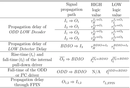
Table 5.1 Pull-down current of open-drain buses. . . 47
Table 5.2 Different states with respect to the voltage level of the BDIO node. . 47
Table 5.3 Delays and rise/fall times of the interface circuit. . . 55
Table 5.4 Design specification of the bi-directional interface in the test-chip ac-cording to I2C Fast-mode Plus protocol. . . 61
Table 5.5 Characterization of the Interface Circuit Based on Post Layout Circuit Simulations. . . 62
Table 6.1 The values of etH and etL from post-layout simulation. . . 83
Table 6.2 Comparison with published compact oversampling A/D converter. . . 92
Table 7.1 Characteristics of the differential interface from post-layout simulation. 109 Table 7.2 Areas of the differential interface and their stages for one four-stages interface unit. . . 110
Table 8.1 Silicon area of the pass transistor based input stage. . . 119
Table 8.2 Comparison between the input stage based on unity-gain buffer multi-plexer and the input stage based on pass-transistor multimulti-plexer. . . . 128
LIST OF FIGURES
Figure 1.1 Generic model of a field programmable interconnection network (FPIN)
in a FPGA. . . 2
Figure 1.2 Conceptual overview of the active reconfigurable board. . . 3
Figure 1.3 Hierarchical description of the active reconfigurable board. . . 3
Figure 1.4 Schematic diagram and propagation path of an electrical signal between two uICs pins in contact with the CIO/Nanopads on the WaferIC. The electrical signal propagates from a source uIC to a destination uIC. . 4
Figure 1.5 Possible uses of enhanced programmable devices (EPDs). . . 5
Figure 2.1 WaferNet showing the connections between neighboring 1, 2, 4, 8, 16 and 32 in all directions. . . 9
Figure 2.2 Architecture of an unit cell [1] with configuration registers, CIOs and crossbar multiplexers. . . 10
Figure 2.3 I2C Bus. . . 12
Figure 2.4 Connection of P82B96/PCA9600 I2C bus extension buffers. . . 13
Figure 2.5 Δ-modulator. . . 16
Figure 2.6 Waveform at various nodes of the Δ-modulation in Fig. 2.5(a). . . 16
Figure 2.7 ΣΔ modulator. . . 18
Figure 2.8 Noise-shaping function for the Σ∆ modulator shown in Fig. 2.7(a) . . 19
Figure 2.9 A third-order ΣΔ modulator. . . 20
Figure 2.10 Comparison between ΣΔ modulators of given technology process node versus area (µm2). . . 21
Figure 2.11 Comparison between ΣΔ modulators of given technology process node versus FoM (pJ). . . 21
Figure 2.12 Asynchronous Σ∆ modulator. . . 23
Figure 2.13 Differential buffer structure. . . 25
Figure 4.1 WaferICTM with ICs deposited: (a) top view, (b) cross section view. . 32
Figure 4.2 I2C Bus. . . 33
Figure 4.3 (a) Proposed interface. (b) Two instances of the interface intercon-nected together. (c) The level sensing buffer to remove the latching problem. (d) Block diagram. . . 35
Figure 4.4 Full schematic of the interface. . . 36
Figure 4.5 Simulation result. . . 37
Figure 5.2 Hierarchical description of the active reconfigurable platform, from
sys-tem level to configurable I/O (CIO). . . 43
Figure 5.3 Example of an I2C-bus configuration. . . 43
Figure 5.4 Each circle represents an interface unit circuit. . . . 45
Figure 5.5 Development of the bi-directional interface unit circuit. . . 45
Figure 5.6 Development of pseudo-ring interconnection topology. Each circle re-presents an interface unit circuit and is labelled IU#. . . 48
Figure 5.7 Logical signal flow diagram. Low Detector module of each interface unit (IU#) is labelled LD. Each BDIO node belongs to the respective interface unit (IU) and represents distinct physical nodes. . . 50
Figure 5.8 Logical signal flow diagram of dual-queue interconnection topology. Two individual queue network are joined together. Each queue net-work have five interface units. Four interface units (labelled IU#) are connected to external ODD and one Master unit (labelled MU). Low Detector module of each interface unit (IU#) is labelled as LD. . . . 52
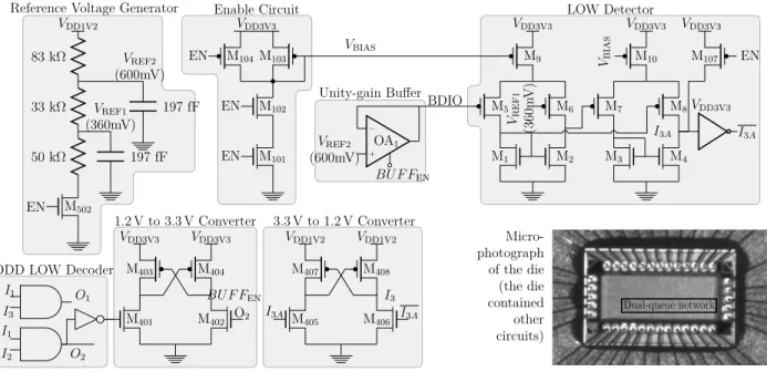
Figure 5.9 Schematic of the interface unit (IU). . . 55
Figure 5.10 Detailed transistor-level schematic of the bi-directional interface unit and micro-photograph of the die. . . 59
Figure 5.11 Dual-queue interconnection topology with 8 interface units implemen-ted in the test-chip. . . 63
Figure 5.12 Measurement result of dual-queue interconnected network (shown in Fig. 5.11) from the test-chip. . . 64
Figure 6.1 Asynchronous ΣΔmodulator. . . 69
Figure 6.2 Generic FPIN model of a Field Programmable Interconnection Network. 70 Figure 6.3 Hierarchical description of the reconfigurable board to CIO. . . 71
Figure 6.4 Different implementations of the generic asynchronous ΣΔ modulator. 73 Figure 6.5 The proposed ADM. . . 75
Figure 6.6 Proposed linear s-domain model of the ADM shown in Fig. 6.5. . . . 76
Figure 6.7 Evaluation of the oscillation frequency of the asynchronous ΣΔ modulator (ASDM). . . 77
Figure 6.8 Input signal frequency is 1 MHz. . . 78
Figure 6.9 High-level simulation with Simulink® of the proposed ADM architec-ture model (Fig. 6.5). Input signal frequency is 1 MHz. Representative component noise sources are included but the RC-filter is ideal. . . . 79
Figure 6.10 ADM-based analog interface. . . 80
Figure 6.12 Schematic of the X-OR gate. . . 83 Figure 6.13 The effect of mismatch between etH and etL on the SNDR. . . 83 Figure 6.14 Detailed block diagram of the proposed ADM-based analog interface. 84 Figure 6.15 Schematic of the ADM & 3.3 V to 1.2 V converter (transmission side). 85 Figure 6.16 Schematic of the D/A converter (receiving side). . . 85 Figure 6.17 Simulation of the proposed ADM based on s-model in Simulink® and
post-layout simulations in Cadence (VDD= 3.3 V) respectively. Simulink® model included the non-linearity of the filter. . . 86 Figure 6.18 Micro-photograph of the die (the die contained other circuits). . . 87 Figure 6.19 Layout of the ADM and LPF to reconstruct the input signal. . . 88 Figure 6.20 Measured DC transfer characteristics from the test-chip (VDD = 3.3 V)
of the asynchronous Δ-modulator shown in Fig. 6.15. . . 88 Figure 6.21 Measured noise performances from the test-chip. . . 89 Figure 6.22 Simulation of the proposed ADM in with noisy power supply to mimic
the actual test-bench scenario. . . 90 Figure 6.23 Comparison between ΣΔ modulators and the proposed Δ-modulator
on technology process node versus Area (µm2) and FoM (pJ). . . 91 Figure 6.24 Measurement result for input frequency of 500 kHz, 1 MHz, and 2 MHz
from the test-chip. . . 95 Figure 7.1 CML structure. . . 98 Figure 7.2 Conceptual overview of the active reconfigurable platform. . . 100 Figure 7.3 Differential pins of user’s ICs interfacing with the NanoPad array of
the WaferIC (zoom of Fig. 7.2(a)) [3]. . . 100 Figure 7.4 Architecture of the embedded differential propagation chain [3]. . . . 102 Figure 7.5 The input differential configurable network. . . 102 Figure 7.6 Tiling of differential interface unit. . . 103 Figure 7.7 Continuous floor plan of the architecture with overlap between adjacent
interface units. Each of the two shaded rectangles can be configured as a differential interface unit. . . 104 Figure 7.8 Schematic of the analog multiplexers. . . 106 Figure 7.9 Configurable differential-to-single-ended converter (the multiplexers in
these two figures are digital multiplexers). . . 107 Figure 7.10 Schematic of the interface output circuit in each NanoPad. . . 108 Figure 7.11 Test-chip. . . 109 Figure 7.12 Measured DC transfer characteristics (VDD = 3.3 V) of the analog
Figure 7.13 Measured eye diagrams at different data rates from test-chip. . . 111 Figure 8.1 Architecture and floor plan of the pass transistor multiplexer based
differential input stage. . . 114 Figure 8.2 Pass-transistor based model. . . 115 Figure 8.3 Differential amplifier with differential output. . . 115 Figure 8.4 Schematic of the differential input stage and differential amplifier with
differential output in stage-4. . . 116 Figure 8.5 Proposed differential-to-single ended converter. . . 116 Figure 8.6 Schematic of the differential input stage with the differential-to-single
ended converter at Stage-4. . . 117 Figure 8.7 Layout. . . 118 Figure 8.8 2 GHz output (vOUT4+ and vOUT4- in Fig. 8.4) of stage-4 multiplexer
from Monte Carlo mismatch variation (typical-typical) simulation. Input (vIN- and vIN+ in Fig. 8.4) common-mode voltage=1.0 V. . . 119 Figure 8.9 2 GHz output (vOUT+ and vOUT-in Fig. 8.4) of stage-4 fully differential
amplifier from Monte Carlo mismatch variation (typical-typical) si-mulation. Input (vIN- and vIN+ in Fig. 8.4) common-mode voltage=1.0 V.120 Figure 8.10 2 GHz output (vOUT+and vOUT-in Fig. 8.4) of Stage-4 fully differential
amplifier from Monte Carlo process variation (typical-typical) simu-lation. Input (vIN- and vIN+ in Fig. 8.4) common-mode voltage=1.0 V. 121 Figure 8.11 2 GHz output (vOUT in Fig. 8.6) of the differential-to-single-ended
converter from Monte Carlo mismatch variation (typical-typical) si-mulation. Input (vIN- and vIN+ in Fig. 8.6) common-mode voltage=1.2 V.122 Figure 8.12 2 GHz output (vOUT in Fig. 8.6) of the differential-to-single-ended
converter from Monte Carlo mismatch variation (typical-typical) si-mulation. Input (vIN- and vIN+ in Fig. 8.6) common-mode voltage=1.6 V.122 Figure 8.13 1 GHz output (vOUT in Fig. 8.6) of the differential-to-single-ended
converter from Monte Carlo mismatch variation (typical-typical) si-mulation. Input (vIN- and vIN+ in Fig. 8.6) common-mode voltage=1.2 V.123 Figure 8.14 1 GHz output (vOUT in Fig. 8.6) of the differential-to-single-ended
converter from Monte Carlo mismatch variation (typical-typical) si-mulation. Input (vIN- and vIN+ in Fig. 8.6) common-mode voltage=2.0 V.123 Figure 8.15 Schematic of the analog multiplexers simulated in IBM 0.13 µm CMOS
technology. . . 125 Figure 8.16 The signal path consisting of 3 multiplexer stages that was simulated
Figure 8.17 2 GHz output (vOUT+/− in Fig. 8.16) of the stage-3 multiplexer from Monte Carlo mismatch variation (typical-typical) simulation. Input (vIN+/− in Fig. 8.16) common-mode voltage=1.6 V and voltage swing
VP-P=800 mV was used. . . 126
Figure A.1 The ASDM used in the proposed analog interface . . . 144
Figure A.2 Waveform of the hysteresis input assuming vin is a DC value and 0 < vin< VDD. . . 144
Figure A.3 Simulated frequency of oscilation (VDD = 3.3 V) of the asynchronous ΣΔ modulator shown in Fig. 6.15 for different vin. . . 145
Figure C.1 Test chip. . . 147
Figure C.2 Bonding diagram of test chip. Package type: CQFP44A. . . 148
Figure C.3 Pin assignment of the test chip. . . 149
Figure C.4 Layout of test chip. . . 149
Figure C.5 Test setup of the bi-directional interface. . . 150
LIST OF ABBREVIATION
ADC analog-to-digital converter. 7
ADM asynchronous Δ-modulator. ix, xiv, 22, 26–28, 67, 68, 129–133
ASDM asynchronous ΣΔ modulator. xv, xviii, xxi, 20, 22, 23, 77, 132, 133, 143, 145, 150
ATCA advanced telecom computing architecture. 5
CIO configurable I/O. viii, 3–6, 11, 12, 24, 25, 28, 29, 112, 113, 116, 125, 126 CLB configurable logic block. 1
CML current mode logic. ix, 6, 28, 29, 112, 114, 118, 123, 126, 131 CT-ΣΔ continuous-time ΣΔ modulator. 22
DAC digital-to-analog converter. 7 DDC display data channel. 5 DLL delay-locked loop. 132, 133
ENOB effective number of bit. 19
EPD enhanced programmable device. 3, 4
FoM figure of merit. 20, 130
FPGA field-programmable gate array. viii, xvii, 1–4, 26, 40, 41, 66, 129 FPIC field programmable interconnection chip. 1
FPIN field programmable interconnection network. viii, ix, xvii, 1–8, 14, 22, 24–29, 39– 47, 54, 56, 57, 59, 60, 66, 112–114, 129, 131
GPIO general purpose input output. 11
HSTL high-speed transceiver logic. 6
I2C Inter-Integrated Circuit. 11 IC integrated circuit. viii, 2
IPMI intelligent platform management interface. 5
LVPECL low voltage positive-emitter-coupled logic. 6
OSR oversampling ratio. 19
PCB printed circuit board. 11, 150 PLL phase-locked loop. 14, 132, 133 PMBus power management bus. 5
SFDR spurious-free dynamic range. 130 SMBus system management bus. 5
SNDR signal-to-noise and distortion ratio. 20, 28, 130 SNR signal-to-noise ratio. 28, 130
SQNR signal-to-quantization noise ratio. 17 SSI stacked silicon interconnect. 1
TSV through-silicon via. 1–3 TTL transistor–transistor logic. 14
uIC user integrated circuit. ix, xvii, 2–4, 6, 8, 9, 11, 13, 25, 28, 29, 113, 114, 116, 118
LIST OF APPENDICES
APPENDIX A . . . 142 APPENDIX B Time Line . . . 146 APPENDIX C Details of Test Chips . . . 147
CHAPTER 1 INTRODUCTION
Following Moore’s law, semiconductor technology scaling has ushered the remarkable pro-gress of microelectronic integration over the past four decades. Every technology generation, introduced every two to three years, has doubled the transistor count per chip, increased the operating frequency by 43%, and reduced the switching energy consumption by 65% on average [4]. Very complex systems with programmability at the user end have been made possible by leveraging such unprecedented logic density increase. A very successful class of configurable integrated circuits enabled by these trends is the field-programmable gate arrays (FPGAs).
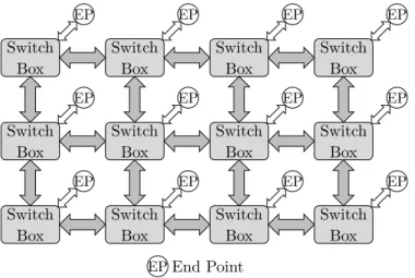
Field programmable interconnection networks (FPINs) are the backbone of emulation and prototyping platforms,i.e. FPGAs, ZeBu Server [5], Veloce verification system [6], Cadence® Palladium® series of accelerators/emulators [7], and many other Network-on-Chip architec-tures [8]. FPINs provide reconfigurable interconnections between various endpoints, i.e. the configurable logic blocks (CLBs) in FPGAs. Any digital hardware can be emulated in FP-GAs partly by reconfiguring their embedded FPINs. However, reconfigurability of the FPINs sometimes entails long interconnects between endpoints that result in excessive propagation delays. Buffers are typically inserted along these on-chip resistive interconnects to ensure fast signal propagation and linear signal delay increase with distance. Once configured, in-terconnects are therefore uni-directional. Systems used for digital hardware emulation can enhance their capability and performance by having programmable interconnection between FPGAs. Commercial logic emulation systems, such as the Realizer system [9], use pro-grammable interconnection devices between FPGAs. These devices are called field program-mable interconnection chips (FPICs). Fig. 1.1 illustrates an example where an FPIN provides programmable interconnections between endpoints (I/O or configurable logic blocks) in an FPGA.
Modern FPGAs, such as those from the Xilinx’s Virtex-7 family [10], can emulate circuits with up to 2 000 000 logic gates and that maximum complexity keeps growing. Some of the large FPGA chips are internally implemented as several smaller connected FPGA dies. By combining through-silicon vias (TSVs) and microbump technology, Xilinx has developed a stacked silicon interconnect (SSI) technology that is the foundation of Virtex-7 FPGAs [11]. Xilinx notably uses a passive silicon interposer to combine multiple FPGA Super Logic Region (SLR). Instead of creating a 3D-stack, the FPGAs are put side-by-side on a passive interposer and hence this technology is called 2.5 D integration. The interposer is built using a
Switch Box Switch Box Switch Box Switch Box Switch
Box SwitchBox SwitchBox SwitchBox Switch Box Switch Box Switch Box Switch Box EP EP EP EP EP EP EP EP EP EP EP EP EPEnd Point
Figure 1.1 Generic model of a field programmable interconnection network (FPIN) in a FPGA.
low-risk, high-yield 65 nm process with four passive layers of metallization. It provides tens of thousands of die-to-die connections to enable ultra-high interconnect bandwidth, less power consumption and one fifth the latency of standard I/Os [11]. This passive interposer does not contain any transistor and hence, it is claimed to be a low risk and low cost device that does not introduce TSV related performance degradations [12].
1.1 Active Reconfigurable Board Overview
In addition to FPGAs, an example of an FPIN-based circuit targeted in this thesis is the active reconfigurable platform named WaferBoard that was proposed in [1]. It was developed as a prototyping platform that provides interconnections among multiple user integrated circuits (uICs) to test and prototype electronic systems. This reconfigurable platform can be easily extended as anactive silicon interposer, because unlike the aforementioned passive interposer of Xilinx, the interconnection network can be dynamically configured like an FPGA. It has an uni-directional switch box based FPIN that can be programmed by the user to interconnect the component uICs. The reconfigurable platform is primarily designed to provide digital interconnections between component uICs. However, as originally proposed, this FPIN-based prototyping platform was not supporting open-drain bi-directional signals (notably used in the I2C protocol and its derivatives [13–16]), analog signals, or differential signals.
The core of the active reconfigurable board is a wafer scale IC (called WaferIC [1]) upon which user component ICs or uICs are to be deposited. The surface and cross-section of the active reconfigurable board is shown in Fig. 1.2(a) & 1.2(b) respectively. The surface of the
uIC1
uIC3
uIC2
(a) Top view.
Solder ball pin Conductive film Bottom support Reconfigurable board uIC Top cover (b) Cross-section.
Figure 1.2 Conceptual overview of the active reconfigurable board.
≈ 1.6 centimeter ≈ 1 milimeter Reticles Inter-reticle stitching CIO or NanoPad
Wafer scale IC
(WaferIC) A reticle :
A sea of cells 2 × 2 cells
Figure 1.3 Hierarchical description of the active reconfigurable board.
wafer scale IC has a dense array of very fine (tens of microns) conducting pads acting as configurable I/Os (CIOs), as shown in Fig. 1.3. These CIOs are called NanoPads in [1]. An FPIN is embedded in the wafer scale IC. The FPIN can be configured, similar to an FPGA, to connect any two CIOs. uIC pins are to have physical contacts with the CIO and communicate through the embedded FPIN as shown in Fig. 1.4. Each CIO has its own configurable I/O buffers. If a CIO is to operate as an input, then the respective CIO is configured as input and this buffer receives the signal from a source uIC and propagates it through the FPIN to other destination CIOs. The destination CIO’s buffer is configured as an output buffer and it propagates the signal to the corresponding destination uIC.
1.2 Enhanced Programmable Devices (EPDs)
Demands for increased density, higher bandwidths, and lower power pushed IC designs to-ward 3D IC encapsulation. 3D ICs are manufactured by stacking multiple silicon wafers and/or dies and interconnecting them vertically. Passive silicon interposers with TSVs and several metallization layers are used to align the micro-beads of each silicon die. These dense interconnections between chip layers present a significant challenge to the alignment, testing and diagnosis. Enhanced programmable devices (EPDs) are conceived as active silicon
inter-WaferIC
source uIC destination uIC
Input Output Power regulator Ground ? ? Input Output Power regulator Ground ? ? 4 4 WafeNet/FPIN
Crossbar Crossbar Crossbar
Multiplexer De-multiplexer
CIO/NanoPad Anisotropic
Film
The gray box denotes the additional interface circuit(s) to support open-drain, analog or
differential signaling.
Figure 1.4 Schematic diagram and propagation path of an electrical signal between two uICs pins in contact with the CIO/Nanopads on the WaferIC. The electrical signal propagates from a source uIC to a destination uIC.
posers that can provide, in addition to configurable interconnections, enhancements in terms of testability and diagnosis. A possible basic structure of an EPD is shown in Fig. 1.5. EPDs are intended to support as many types of signal interfaces as possible. As envisioned, similar to the aforementioned WaferBoard [1], an EPD surface has a dense array of CIOs and each CIO is connected to an internal FPIN that can be configured to connect a CIO to any others.
1.3 Motivation
Configurability of FPINs is extensively utilized in FPGAs, in prototyping platforms, and in many network-on-chip architectures. This thesis work was motivated by the observation that the application domains of such FPIN-based prototyping and emulation platform could be significantly broadened by supporting open-drain bi-directional signals, analog signals, and differential signals. Three interface circuits were thus elaborated and developed to support reconfigurable routing of open-drain bi-directional, analog or differential signals through a uni-directional digital FPIN. Even though the need for such interface circuits were originally conceived in the context of the WaferBoard [1], the developed interface circuits can be inte-grated in or with FPGAs, active silicon interposers (i.e. EPDs) or any platform that embeds some digital FPINs.
TSV
PCB EPD Component (packaged)
(a) Basic structure.
PCB 3D component EPD EPD EPD Bare die - 1 Bare die - 2 Bare die - 3 (b) 3D integration. PCB 2.5D component EPD Bare die - 2
Bare die - 1 Bare die - 3
(c) 2.5 D Integration.
Figure 1.5 Possible uses of enhanced programmable devices (EPDs).
1.3.1 Open-drain Bi-directional communication
Multi-master bi-directional communication is widely used in electronic communication sys-tems. It is used between low-speed peripherals and a motherboard, in embedded systems, in cellphones, and in many other electronic devices. The most widely used bi-directional bus is the I2C protocol. Several other communication standards are derived from the I2C protocol [15, 16]. Some of these I2C derived standards are the:
1. System management bus (SMBus) [16]. 2. Power management bus (PMBus) [17].
3. Intelligent platform management interface (IPMI) [18]. 4. Display data channel (DDC) [19].
5. Advanced telecom computing architecture (ATCA) [20].
The main principle of the I2C protocol is that it is an open-drain (or open-collector) bus. All the derived protocols depend on the “wired AND” property of open-drain (or open-collector) connections. FPINs cannot directly support such “wired AND” connections, because each interconnection link is established by uni-directional binary digital signaling. Additional in-terface circuits are required at the CIOs or endpoints to support “wired AND” connections to outside world while the internal connections inside the FPIN is established by uni-directional digital buffers and switch boxes (multiplexers).
1.3.2 Analog Signal Communication
The WaferBoard [1] was primarily developed to prototype digital electronic systems. Ho-wever, nowadays many electronic systems are at least partly mixed-signal systems. Having the ability to reconfigurably route analog signals through the embedded FPIN can greatly improve the versatility of the WaferBoard or any electronic system prototyping platforms. In the context of the WaferBoard, A/D (transmitter) and D/A (receiver) converters are required to support analog signal propagation through the digital FPIN. The A/D converter receives the input analog signal from the transmitting user integrated circuit (uIC) and converts it into a digital format that can be propagated through the digital FPIN to the receiving side. This receiving side must comprise a D/A converter that can reproduce the original analog signal and provide it to the receiving uIC. However, due to the stringent limitations on the available silicon area, a very compact implementation of A/D and D/A converter is required for compatibility with the WaferBoard. Thus, the author was motivated to find a compact A/D and D/A converter solution that can support reconfigurable routing of analog signals within the existing constraints of the WaferBoard [1].
1.3.3 Differential Signal communication
Differential signaling is widely used in high speed data transmission. It sends an electrical signal and its complement as a differential pair of signals through two conductors. External electromagnetic interferences tend to affect both conductors similarly and the receiving end only detects the difference between the conductors. Thus, differential signaling mitigates com-mon mode electromagnetic coupling that affects single-ended signaling. Standards, currently in use for differential signaling, include for instance low voltage differential signalling (LVDS), low voltage positive-emitter-coupled logic (LVPECL), CML, and high-speed transceiver logic (HSTL) [21].
A differential interface must achieve spatial reconfigurability to support differential signa-ling in a FPIN-based prototyping platform such as the WaferBoard [1]. As uICs can be randomly placed on the active surface of the WaferBoard, the corresponding “contacted” CIOs/NanoPads can have random physical locations. The differential interface must have the ability to support such randomly located CIOs/NanoPads and still maintain the requi-red symmetry and signal integrity of high-speed differential signaling. The operating speed of standard differential signaling is higher than the target operating speed of the prototyping platform. The primary target of the differential interface for the prototyping platform is for versatility purpose rather than supporting the highest possible speed.
1.4 High Level Objectives of This Research
The aim of this research is :
1. To develop an interface that can support open-drain interconnection based bi-directional buses (such as I2C) in any digital FPIN-based prototyping platform.
2. To develop an interface that can support analog signal transmission in the WaferBoard [1] according to WaferBoard’s constraints (see Sec.2.1.2).
3. To develop an interface that can support differential signal transmission through the single-ended digital FPIN of the WaferBoard.
1.5 Organization of Thesis
This thesis is organized as follows. Chapter 2 presents background information and related previous works, with a brief overview of the prototyping platform [1], open-drain inter-connection based bi-directional bus, analog-to-digital converters (ADCs), digital-to-analog converters (DACs), and differential signalling. Chapter 3 presents the detailed organization of the thesis while Chapters 4−8 constitute the core of the thesis. Chapter 9 presents a general discussion on the entire thesis. The contributions from this thesis are finally summarized and possible future works are discussed in Conclusion.
CHAPTER 2 BACKGROUND INFORMATION AND RELATED PREVIOUS
WORKS
A brief review of the FPIN-based prototyping platform [1] will facilitate the reader to pro-perly understand the topic discussed in this thesis. Characteristics of open-drain, analog, and differential signalling are reviewed in the perspective of the prototyping platform to support explanation of the the proposed solutions. Sec. 2.1 describes the prototyping platform and its various constraints imposed to interface circuits. Sec. 2.2 presents an overview of open-drain interconnection based bi-directional buses. Sec. 2.3 presents different types of A/D and D/A converters, and considers their feasibility for the digital FPIN-based prototyping platform [1]. Sec. 2.4 presents various constraints of differential signaling in the target environment of the digital FPIN-based prototyping platform [1].
2.1 Active Reconfigurable Platform [1]
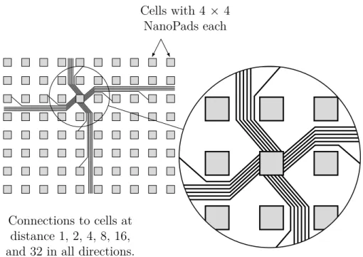
The WaferIC shown in Fig. 1.3 is the core of an active reconfigurable platform [1]. Component uICs are to be placed on the surface of the WaferIC. The building block of the WaferIC is called a unit cell. Each unit cell contains an array of 4 × 4 CIO, I/O buffers, routing and control circuitries, and a multiplexer-based crossbar. This crossbar routes incoming signals to one of the CIOs, belonging to itself or to other unit cells. When a signal is propagated through the WaferIC, it is routed from unit cell to unit cell until it reaches the destination CIO and the corresponding uIC pin [1]. The dimension of each unit cell is 560 µm × 560 µm [1]. These cells are tiled within a reticle, and the WaferIC is built from repetition of this reticle across the entire wafer.
2.1.1 WaferNet
Each unit cell is connected to an embedded digital FPIN, called WaferNet, as shown in Fig. 2.1, that can be configured to connect any two unit cells, whatever their position is. In other words, any two CIOs belonging to any two unit cells can be connected by the WaferNet. Each unit cell has connections with other unit cells which are 1,2,4,8,16, and 32nd unit cells away in all fours directions, as shown in Fig. 2.1. An uIC pin (or solder ball) can be contacted to several CIOs. The WaferIC detects and maps the contacted pins, and a netlist is generated according to the required connections. Then the WaferNet is configured to provide
9
Connections to cells at distance 1, 2, 4, 8, 16, and 32 in all directions.
Cells with 4 × 4 NanoPads each
Connections to cells at
distance 1, 2, 4, 8, 16,
and 32 in all directions.
NanoPads each
Figure 2.1 WaferNet showing the connections between neighboring 1, 2, 4, 8, 16 and 32 in all directions.
all required connections between the uICs according to the netlist [1].
The routing of signals through the WaferNet, from a unit cell to another unit cell is ac-complished by digital multiplexer-based crossbars. Each CIO has its own buffers. If a CIO is to operate as an input, then the respective I/O buffer is configured accordingly and this buffer receives the signal from a uIC and propagates it to the embedded crossbar of the local unit cell to which it belongs. The crossbar routes the signal to the link pointing toward the destination CIO’s unit cell. Since the signal path can make a “jump” of only 1,2,4,8,16, and 32 unit cells at a time, it usually takes several jumps in all four directions for the signal to reach some arbitrary destination unit cell. At the destination cell, the CIO buffer is confi-gured as an output buffer. All I/O buffers must be explicitly conficonfi-gured, either as an input or an output buffer. Normally this configuration is done before “testing” or “prototyping” with uICs. After CIOs are configured, the state remains unchanged during the entire period of testing or prototyping operation.
2.1.2 Silicon Area Constraints of WaferIC
The functional architecture of the unit cell is depicted in Fig. 2.2. If any additional features are intended to be added, it must be fitted into the unit cell’s dimension of 560 µm × 560 µm only that translates into an area of 313600 µm2. This area is already overstretched by the CIO
Configurable I/O (CIO) Contact detection block Power supply block 4 × 4 CIO array To next cell De-m ultiplexer Multiplexer Configuration register The thick gray arrow-line though the confi-guration registers is the JTAG chain Programmable crossbar Crossbar core T o other cells F rom other cells Multiplexers From previous cells From previous cell To next cell
Figure 2.2 Architecture of an unit cell [1] with configuration registers, CIOs and crossbar multiplexers.
buffers, crossbar multiplexers, configuration registers of the JTAG chain, and other control circuitry. Thus, any additional circuitry must be very compact as something else needs to be compressed accordingly. Table 2.1 shows the area usage of each blocks of an unit cell in a test-chip that was previously fabricated in TowerJazz’s1 0.18 µm CMOS technology. From the experience, gathered during the design of this test-chip, it appears that any additional features can at most consume 2-3% of the total area of the unit cells. Previous work [22] from other members of the DreamWafer team led to an analog interface circuit based on the frequency modulation of ring oscillator based voltage controlled oscillators (VCOs). The analog interface circuit occupied 4350 µm2 that represents ≈1.4% of the total area of an unit cell. An important consideration is that the interface must be integrated at the “wafer-scale”. Thus, the circuits must be very robust against process variation and if possible defect tolerant. Redundancy at the architectural [1] level has been used to isolate physical defects
Table 2.1 Area of an unit cell in a test-chip that was previously fabricated in TowerJazz’s 0.18 µm CMOS technology. Area (µm2) /Unit Number of ins-tance/Unit Required area ( µm2) Configuration registers of the
JTAG chain 96 490 46944
CIO buffers and power supplya 8892 16 142272
Analog Interfaceb 4350 1 4350
Crossbar multiplexers and other
logicc — — 120000
Total area 313600
a. CIO buffers were clustered with the power supply circuit because CIOs were designed to provide power
supply to uICs. Power supply comprised bandgap circuits and D/A converters used as digitally controlled variable power supply.
b. This analog interface was introduced in [22]. It will be described in Sec. 2.3. c. These circuits were distributed throughout the unit cell.
in WaferIC.
2.2 Bi-Directional Interface
During the 1980s, as electronic systems became more complex with many peripheral connec-tions, direct connection between each components were becoming too complicated because it required a large number of printed circuit board (PCB) traces and general purpose input output (GPIO), notably in the microprocessors. A multi-master bi-directional protocol was required to solve this problem, where every entity can send and receive data through a “single” physical line. The Inter-Integrated Circuit (I2C) bus is such a communication standard.
2.2.1 I2C Bus
The I2C protocol is a multi-master bidirectional serial bus developed by Philips [14]. This communication standard is used in various control architectures such as the System Manage-ment Bus (SMBus) [16], the Power ManageManage-ment Bus (PMBus) [17], the Intelligent Platform Management Interface (IPMI) [18], Display Data Channel (DDC) [19], and the Advanced Telecom Computing Architecture (ATCA) [20]. I2C [14] uses two bidirectional open-drain (or open-collector) lines named Serial Data Line (SDA) and Serial Clock Line (SCL). Both lines have external pull-up resistors. In the I2C protocol (shown in Fig. 2.3), when a
com-SDA SCL VDD VDD A/D converter LCD Driver Gate Array
Micro-Controller IC-1 IC-2
Figure 2.3 I2C Bus.
ponent wants to output HIGH, the output driver does not output an explicit HIGH. Rather, the output driver releases the bus and an external common pull up resistor pulls up the bus to VDD. When a component wants to output a LOW, it explicitly drives the bus to LOW because the pull down capability of the driver is much stronger than the pull up resistor. The I2C protocol has no explicit signal to specify the direction of data in the bus. Rather there are some rules embedded in the protocol like clock synchronization, arbitration, and
clock stretching [14], rules by which an I2C driver connected to a bus “realizes” when it is allowed to write into the bus, read from the bus or stay idle. All those rules are based on the “wired AND” property of open-drain connection. If only one of the connected drivers outputs a LOW on the bus, the bus will become LOW. In the I2C protocol, there is no single master controller. It is a multi-master bus where any one of the connected components can assume the role of master and can control the direction of the data. Such communication protocol cannot be supported by the previously reported version of the WaferIC [1].
The I2C bus is not a synchronous communication system. Even though each transmission between two components is controlled by a clock signal, that clock is provided by the respec-tive master. From the perspective of the entire system, there is no master clock. Thus, any interface circuit at the CIO of the unit cell in WaferIC, mimicking “wired AND” intercon-nection to the outside world, cannot be operated by any master clock to periodically check the voltage level at the corresponding CIOs. The interface circuit must be asynchronous in the sense that, whenever an external I2C driver pulls down the voltage level to LOW, the interface must immediately detect it and send the information to other connected interface units. This detection and transmission is not challenging. The challenge is, sending LOW signal to other interface units makes their corresponding CIOs LOW and subsequently they send LOW signal(s) back. Thus, a “state-latching” phenomenon occurs and even when the external I2C driver releases the corresponding CIO, the CIO voltage might still be held down
Long Wire Gro up -3 P82 B9 6 / PC A9 6 0 0 I 2 C/ Driv er I 2C/ Driv er G rou p -1 P 8 2 B 9 6/ P C A 9 60 0 I2 C/ Driv er I 2 C/ Driv er Group-2 P82B96/ PCA9600 I2 C/ Driver I2C/ Driver
Figure 2.4 Connection of P82B96/PCA9600 I2C bus extension buffers.
to LOW. If a master clock could have been used to control all the interface units, then some trigger could have been used to pull out the entire system from this state-latching. Thus, developing an asynchronous interface (without any master clock) that can behave like an open-drain interconnection to the external I2C drivers (uIC), while preventing “state-latching”, is a challenging task. The situation is further exacerbated by the constraints of the WaferIC.
Since WaferBoard is a recent innovation, references to compatible interface circuits are not available in the literature. To the best of our knowledge, no comparable interface circuit mimicking the behaviour of an open-drain connection has been reported in the literature. The closest existing circuits that we found are the P82B96 [23] and PCA9600 [24], two com-mercially available I2C bus extension buffers. Even though these circuits are not equivalent to the aim of this research, they have some similarity in their use of double interpretation voltage levels below 0.3 VDD to avoid a state-latching phenomenon.
Fig. 2.4 shows the connection of P82B96/PCA9600 I2C bus extension buffers that connect multiple isolated groups of I2C drivers. The P82B96 bus extension buffer can interface I2C logic signals to similar buses having different voltage and current levels [23]. The PCA9600 is intended to isolate I2C-bus capacitance, therefore allowing long wires with higher loading capacitance than the I2C specifications to be driven [24]. PCA9600 can drive load of up to 4000 pF. The PCA9600 is a higher-speed version of the P82B96. It creates a non-latching, bidirectional, logic interface between a normal I2C-bus and a range of other higher capaci-tance and different voltage bus configurations. It can operate at speeds of up to 1 MHz, and
the high drive side is compatible with the I2C Fast-mode Plus (Fm+) specifications. The PCA9600 features temperature-stabilized logic voltage levels that allows interfacing with I2C-derived buses such as SMBus, PMBus, or with microprocessors that use those same transistor–transistor logic (TTL) logic levels.
2.3 Analog Interface
The WaferBoard was primarily developed to prototype digital electronic systems. Nowadays though most of the communication and signal processing is done in the digital domain, data acquisition systems and power supply components still are essentially analog devices. Prototyping and testing systems comprising such devices require analog interconnectivity. Thus, WaferBoard must have the ability to sense the voltage level from one end point and reconfigurably route that “information” through the embedded FPIN to another end point to prototype such systems. In general, an analog interface circuit reconfigurably routing an analog signal through a digital FPIN must comprise A/D (transmitter side) and D/A (receiver side) converters. A source IC provides an analog signal at one end point to the A/D converter (transmitter). The A/D converter transforms it into a digital format that will be reconfigurably routed through the FPIN to the D/A converter (receiver side). The digital data, upon reaching the D/A converter, is transformed back into a reconstructed copy of the original analog signal and provided to the destination IC at another end point.
A solution was introduced in [22] to provide reconfigurable routing of analog signals in the WaferBoard [1]. The solution used frequency modulation of ring oscillator based VCOs that converted analog signals into discrete-valued pulses that could be reconfigurably routed through the FPIN. The analog signal was reconstructed (demodulated) from the discrete-valued pulses by a phase-locked loop (PLL). However, due to non-linearities in the voltage to frequency transfer curve of ring oscillator based VCOs, that solution could support input analog signals in the range of only 0.6-1.6 V for a power supply of 1.8 V and a bandwidth of 200 kHz [22]. Thus, the author of this thesis was motivated to find an alternative A/D and D/A converters solution that can overcome the drawbacks of the aforementioned analog interface within the existing constraints of the WaferBoard.
2.3.1 Analog to Digital Converter
Both A/D and D/A converters can be classified into two main categories. 1. Nyquist-rate and
In the first category, there exists a one-to-one correspondence between the input and output samples. Each input sample is processed, without any regard to the earlier (or later) input samples. In other words, this type of converters has no memory. Due to the one-to-one corres-pondence between each input sample and the corresponding output sample, the resolution of the quantizer has to be as high as possible to keep the quantization noise low. The sampling rate can be as low as the Nyquist’s criterion, i.e., twice the bandwidth of the input signal. Due to limitations of electronic circuits, such as the finite gain-bandwidth of amplifiers and finite roll-off of low-pass filters, the actual sampling rate must be slightly higher than this minimum value. Nyquist-rate converters require high-accuracy analog components (amplifier, resistors, current sources or capacitors) in order to achieve acceptable linearity and accuracy. Thus, Nyquist-rate converters are often difficult to implement in scaled CMOS technology because of low supply voltages and poor transistor output impedance (due to short-channel effects) [25].
In oversampled converters, the sampling rate is higher than the Nyquist-rate and each input sample is processed with regard to a few previous sample(s). In other words, this type of converters has memory. Due to taking into consideration of the previous samples, the re-solution of the quantizer can be lower. ΣΔ modulator and Δ-modulator are two types of oversampling converter that require low-resolution quantizer (usually 1-bit). Because of over-sampling, oversampled converters can trade the extra samples for resolution in amplitude. Thus, mismatch in analog circuits can be tolerated. The use of higher sampling rate also eliminates the need for high roll-off in the analog anti aliasing filter at the input to the A/D converter, as well as in the low-pass filters in the D/A converter [26, 27]. The possibility of 1-bit output in ΣΔ modulator and Δ-modulator make them particularly suitable A/D conver-ters for reconfigurable routing of analog signal in the FPIN-based prototyping platform [1] because it obviates parallel-to-serial and serial-to-parallel conversions at the transmitting and receiving side respectively.
2.3.2 Δ-Modulator
A Δ-modulator is shown in Fig. 2.5(a). It utilizes an internal low-resolution quantizer (or A/D converter), a loop filter and a D/A converter in a feedback loop. Replacing the quantizer by its linear model, the corresponding z-domain (discrete-time) model of the Δ-modulator is shown in Fig. 2.5(b). A Δ-modulation waveform is shown in Fig. 2.6. The input waveform (u in Fig. 2.5(a)) is approximated by a “staircase” signal (ˆu in Fig. 2.5(a)) by the Δ-modulator.
The step size of the staircase signal is fixed to a constant value e. The difference between
+ A/D Converter D/A Converter Z u v − ˆ u
(a) Block diagram.
+ + E(z) z−1 1 − z−1 U(z) V(z) − ˆ U (z)
(b) Linearized z-domain model. Figure 2.5 Δ-modulator. 0 2Ts 4Ts 6Ts 8Ts 10Ts 12Ts 14Ts 16Ts 18Ts Binary 1-bit sequence 1 0 1 1 1 1 1 1 0 1 0 1 0 0 0 0 0 e =step size Time Amplitude → u (input) ˆ u (approximated input) v (digital output)
Figure 2.6 Waveform at various nodes of the Δ-modulation in Fig. 2.5(a).
or “hunt” u properly. Such phenomenon is called slope overload error. By using higher fs
(or smaller Ts), ˆu can be made track u properly. The equivalent mathematical condition of
proper tracking or “hunt” is
max ( du dt ) < e Ts (2.1) Assuming, u = A cos(2πf t + θ) (2.2) Eq. 2.1 becomes 2πf A < e Ts = efs (2.3)
To avoid slope overload error, the maximum amplitude of the input sinusoidal signal has to follow the following inequality,
Amax < e 2π ( fs f ) (2.4) If it is assumed that the spectral power density of the quantization noise (e) is uniformly distributed, then the mean power of the quantization noise is
Pe_total = 1 2e Z e −eε 2(t)dε(t) = e3 3 (2.5)
If the Δ-modulator output is passed though a reconstruction filter with bandwidth of B, the in-band power of the quantization noise is
Pδ= 1 3 B fs ! (e2) (2.6)
Comparing the in-band quantization noise power with the signal power, some mathematical manipulation between Eq. 2.4 and Eq. 2.6 [28] leads to the following expression of signal-to-quantization noise ratio (SQNR) in a Δ-modulator.
SQNR = 3
8π2 ×
fs3
Bf2 (2.7)
Here, B = Bandwidth of the receiving low pass filter
fs = Sampling frequency (2.8)
f = Input signal frequency
It can be seen that the SQNR is inversely proportional to the square of the input frequency. The dependency of the SQNR of a Δ-modulator on the input frequency is a disadvantage compared to ΣΔ modulator. However, Δ-modulator can provide some practical advantage in terms of implementations compared to ΣΔ modulator (detailed explanation in Chapter 6).
2.3.3 ΣΔ Modulator
A ΣΔ modulator is shown in Fig. 2.7(a). It utilizes a feedback loop containing a loop filter, an internal low-resolution quantizer or A/D converter, and a D/A converter. Corresponding z-domain (discrete-time) model of the ΣΔ modulator is shown in Fig. 2.7(b). Analysis gives,
![Figure 2.2 Architecture of an unit cell [1] with configuration registers, CIOs and crossbar multiplexers.](https://thumb-eu.123doks.com/thumbv2/123doknet/2333337.32184/33.918.176.745.102.620/figure-architecture-unit-configuration-registers-cios-crossbar-multiplexers.webp)