HAL Id: hal-00849363
https://hal.archives-ouvertes.fr/hal-00849363
Submitted on 30 Jul 2013HAL is a multi-disciplinary open access archive for the deposit and dissemination of sci-entific research documents, whether they are pub-lished or not. The documents may come from teaching and research institutions in France or abroad, or from public or private research centers.
L’archive ouverte pluridisciplinaire HAL, est destinée au dépôt et à la diffusion de documents scientifiques de niveau recherche, publiés ou non, émanant des établissements d’enseignement et de recherche français ou étrangers, des laboratoires publics ou privés.
Phase noise modelling and optimisation of microwave
SiGe amplifiers for sapphire oscillators applications
Sébastien Gribaldo, Rodolphe Boudot, Gilles Cibiel, Vincent Giordano,
Olivier Llopis
To cite this version:
Sébastien Gribaldo, Rodolphe Boudot, Gilles Cibiel, Vincent Giordano, Olivier Llopis. Phase noise modelling and optimisation of microwave SiGe amplifiers for sapphire oscillators applications. 19th European Frequency and Time Forum, Mar 2005, Besançon, France. pp.343-347. �hal-00849363�
Phase noise modelling and optimisation of microwave SiGe amplifiers
for sapphire oscillators applications
S. Gribaldo
1, R. Boudot
2, G. Cibiel
3, V. Giordano
2, O. Llopis
11
LAAS-CNRS, 7 av. du Colonel Roche, 31077 Toulouse, FRANCE
2Institut FEMTO-ST, dept. LPMO, 32 av. de l Observatoire, Besançon, FRANCE
3CNES, 18 av. Edouard Belin, 31401 Toulouse, FRANCE
Abstract
The nonlinear modelling of different microwave SiGe bipolar transistors has been performed. Using these models, the phase noise of an amplifier is computed, taking into account two different types of noise, the microwave additive noise floor and the up-converted 1/f noise. The simulation technique combines different approaches available in a commercial CAD software. Theoretical results are then compared to the experiment, both for a single stage amplifier and a two stage amplifier. Finally, the phase noise of an optimised sapphire oscillator is calculated.
I. Introduction
Optimizing a low phase noise oscillator is still a very difficult task. One of the possible approaches is to focus on the phase noise of the amplifier included in the feedback loop, which is the main cause of phase noise in microwave oscillators. Inside the cavity bandwidth, the amplifier phase noise is simply converted into oscillator frequency noise, as described in Leeson s paper [1]. Thus, any improvement of the amplifier phase noise results directly in an improvement of the oscillator frequency noise. The advantages of studying amplifier phase noise instead of oscillator phase noise are numerous. Firstly, it is easier to simulate (and optimize) an open loop circuit (an amplifier) than a closed loop circuit (an oscillator). The frequency is indeed externally imposed in an open loop circuit, and this facilitates the convergence of the algorithm. Secondly, the phase noise measurement of an amplifier is possible from the linear behaviour (low input power) up to strong compression, whereas the oscillator can only be measured in compression [2]. Studying phase noise on such a large input power range leads to very interesting information on the device, and is the best way to check the validity of a modelling approach [3]. Moreover, there is no phase loop effect in an amplifier (this parameter is always difficult to control in an oscillator experiment).
This paper focus on the phase noise modelling of different commercially available microwave bipolar transistors (hereafter referenced as TB1 and TB2), all of silicon-germanium (SiGe)
type. The transistors have first been modelled using a conventional large signal model extraction technique. Then the noise sources have been added to the device model and the phase noise has been simulated using dedicated techniques and a commercial harmonic balance software. Finally, the phase noise of various amplifiers is simulated, and the interest of some two stages circuits to get simultaneously low phase noise and high gain performance is pointed out.
II. Devices nonlinear modelling
Our models are based on the classical SPICE Gummel-Poon model [4], to which extrinsic passive elements are added in order to take into account the device fixture. The model is extracted from DC or pulsed I(V) characterization and multi-bias S parameters measurements. It is validated in linear and nonlinear regime, using respectively S parameter data and output power versus input power data at different harmonic frequencies (Figures 1 and 2). There is in both cases a good agreement between the measured and the simulated values, which allows us to go further in complexity by adding the noise parameters to the model.
III. Transistor noise modelling
Phase noise in a transistor, or an amplifier, is the results of two different processes [5]. The first one is the conversion close to the carrier of the device low frequency (LF) noise. The second one is the addition of the high frequency (HF) noise. The two processes acts very differently on the phase noise. The LF noise conversion is a multiplicative process, which means that the noise level follows the signal level. The HF noise is additive, and has thus a minimum impact on phase noise at high signal level.
Both noise processes have to be taken into account in order to be able to accurately simulate the amplifier phase noise (and also, in a second step, the oscillator phase noise).
The HF noise addition is probably easier to model than the LF noise conversion. At low input power, it can be calculated using equation (1).
( )
( ) P FkT f S in 1 = φwhere F is the amplifier noise figure, k the Boltzman constant, T the absolute temperature and
Pin the amplifier input power. However, some
problems arise at high input power. The device noise figure is increased because of device compression [5] (a nonlinear noise figure can be defined). Two approaches can then be used to model the amplifier additive phase noise : either the nonlinear noise figure has been measured in some way [5], and is used to calculate, with equation (1), the phase noise, or a nonlinear noise simulation is performed with a dedicated software (see next paragraph) and using the device natural HF noise sources (resistors thermal noise and junctions schottky noise).
Identifying the LF noise sources in a transistor is a more difficult task. Moreover, active device electrical models are often far from device physics, and finding the right location in the model of a given LF noise source is almost impossible. Locating the noise sources is a prerequisite to phase noise simulation because, in nonlinear operation, the classical equivalent noise source approach is not valid. As an example, a noise source which affects a nonlinear element will be converted, and another noise source which is at the transistor output can be very weakly converted [3]. Moreover, the noise source itself can be affected by the RF large signal, even if the time constants involved in the LF noise generation are very slow compared to the signal period. In other words, the noise does not depend only on the transistor DC conditions (even if these conditions include the rectification of the microwave large signal) [6]. The way to take into account these effects in an equivalent circuit model is still a disputed subject. The noise source can be associated to a nonlinear element of the equivalent circuit [3], or considered itself as nonlinear [7]. However, an equivalent model is by no means a rigorous representation of devices physics, and the only accurate solution to this problem could be in physical approaches [6] or microscopic models. But these models cannot be used directly to compute the noise in a complex system like an oscillator.
Our approach of the problem is a little different. It uses transistor extrinsic LF noise sources, but the effect of the large signal on these noise sources is taken into account : the device LF noise is measured under large signal conditions. This approach is not completely rigorous, because the LF noise measurement is rarely performed in the same conditions that are experienced by the device in oscillator or amplifier operation. However, it has already proven its efficiency [8], and it is simple enough to authorize a circuit optimisation with the device model.
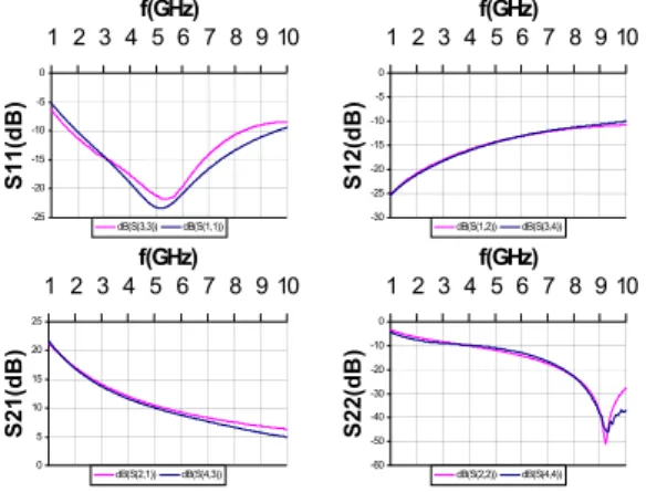
-25 -20 -15 -10 -5 0 1 2 3 4 5 6 7 8 9 10 f(GHz) S1 1 (d B ) dB(S(3,3)) dB(S(1,1)) -30 -25 -20 -15 -10 -5 0 1 2 3 4 5 6 7 8 9 10 f(GHz) S1 2 (d B ) dB(S(1,2)) dB(S(3,4)) 0 5 10 15 20 25 1 2 3 4 5 6 7 8 9 10 f(GHz) S2 1 (d B ) dB(S(2,1)) dB(S(4,3)) -60 -50 -40 -30 -20 -10 0 1 2 3 4 5 6 7 8 9 10 f(GHz) S2 2 (d B ) dB(S(2,2)) dB(S(4,4))
Figure 1 : Comparison between model and
measurement [S] parameters of TB1 (Vce = 2V and Ic= 10 mA )
-10 -8 -6 -4 -2 0 2 4 6 8 10 -25 -20 -15 -10 -5 0 5 10 Pin (dB m) P out ( dB m )
pout 10mA HI Harmonic 1 ADS Harmonic 1
-50 -45 -40 -35 -30 -25 -20 -15 -10 -5 0 -25 -20 -15 -10 -5 0 5 10 Pin (dBm) Ps ( d B m )
pout 10mA HI Harmonic 2 ADS Harmonic 2
-70 -60 -50 -40 -30 -20 -10 0 -25 -20 -15 -10 -5 0 5 10 Pin (dBm) P out (dB m )
pout 10mA HI Harmonic 3 ADS Harmonic 3
-70 -60 -50 -40 -30 -20 -10 0 10 20 -25 -20 -15 -10 -5 0 5 10 Pin (dBm) P out (dB m )
pout 10mA HI Harmonic 1 pout 10mA HI Harmonic 2 pout 10mA HI Harmonic 3 ADS Harmonic 2 ADS Harmonic 3 ADS Harmonic 1
Figure 2 : Comparison between model and
measurement TB1 output power Pout vs. input power
Pin (Vce = 2V and Ic= 10 mA)
Two extrinsic noise sources are generally considered in a classical (linear) bipolar transistor model: the base voltage noise source and the base-emitter current noise source. The base-base-emitter current noise has a physical meaning. It is related to the current flowing in the base-emitter junction, and is composed of a 1/f component, proportional to this current, and a schottky noise floor. This is, in Spice models, the unique 1/f noise source in the transistor. The effect of the base current noise on phase noise is very strong. Actually, in many oscillators, the 1/f frequency fluctuations can be described entirely as a nonlinear conversion of this unique LF noise source. However, it is possible to minimize its effect using a bypass with a high value capacitance [9] or a low impedance bias network [8]. In this case, all the current noise flows into this bypass, and the nonlinearity control voltage is stabilized. What is remaining is the base voltage noise source, which takes into account the voltage fluctuations taking place at the base or the emitter electrodes, but also many other intrinsic fluctuations in the device (it is an equivalent noise source). It is this source that has been characterized, in our modelling approach, versus the microwave input power. The device, used in common emitter
configuration and loaded onto 50 Ω, is fed by a
behaviour is analyzed through bias Tees in a conventional way (i.e. using a low noise amplifier on the collector access).
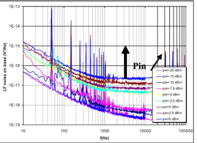
Figures 3 shows this type of measured data for a SiGe bipolar device. The equivalent input voltage noise is measured from linear (or even static) condition up to more than 10 dB compression. A sudden increase of the noise is observed when the device enters into compression. This effect has to be taken into account in the device model (if not, the simulated phase noise would be lower of 10 dB to 15 dB compared to the measured phase noise).
1E-19 1E-18 1E-17 1E-16 1E-15 1E-14 1E-13 10 100 1000 10000 100000 f(Hz) L F n o is e o n b a s e ( V ²/ H z ) pin=-20 dBm pin=-15 dBm pin=-10 dBm pin=-7,5 dBm pin=-5 dBm pin=-2,5 dBm pin=0 dBm pin=2,5 dBm pin=5 dBm r u
Figure 3 : LF equivalent input voltage noise
spectral density ; device TB1, with input microwave power varying from 0 (quiescent device) up to +5 dBm (Ic = 10mA, Vce = 2 V)
In order to model the LF noise increase with the microwave power, two empirical functions
of the microwave power Pin have been used : k1(Pin)
and k2(Pin). The voltage noise dependence on Pin is
described using the following formula :
S (P )=(S +k (P )*S )*(1+k (P ))
V in V 1/f 1 in V floor 2 in (2)
Sv1/f and Svfloor being the spectral power
densities (1/f and noise floor) measured on the quiescent device.
Fitting the noise spectra (Figure 4) leads to the following expressions for these two functions :
1 1 1 P in ( ) 1 b k = a *(e - ) 1 c 2 2 2 P in ( ) 1 b k =a *(e - ) 2 c (3) which are depicted in Figure 5.
Adding this nonlinear noise source to the transistor nonlinear electrical model allows us to simulate both amplifier and oscillator phase noise.
1E-19 1E-18 1E-17 1E-16 1E-15 1E-14 1E-13 10 100 1000 10000 100000 f(Hz) L F n o is e (V ²/ H z ) Sv th_-20 Sv th_-5 Sv th_5 pin=-20 dBm pin=-5 dBm pin=5 dBm
Figure 4 : LF equivalent input voltage noise
spectral density ; device TB1 ; measured and modeled 0 5 10 15 20 25 -25 -20 -15 -10 -5 0 5 10 Pe (dBm ) K f a c to rs k1 f it k2 f it
Figure 5 : k1 and k2 vs. 3.5 GHz input power
variations, (Ic = 10mA, Vce = 2 V) device TB1
IV. Phase noise simulation
The above described model is implemented on a commercial software : Agilent ADS. Various approaches may be used on ADS to simulate phase noise. However, many of these tools are restricted to oscillator simulation ( pnmx and
pnfm ) and special techniques must be implemented to simulate an amplifier phase noise. The first one is the quasi-static perturbation technique, which consist in introducing a small static voltage (or current) shift to evaluate the effect of a LF voltage (or current) noise on the phase of the microwave signal through the amplifier (this is the equivalent of the ADS pnfm technique in oscillator simulation). The second one takes advantage of the ADS envelope simulator , which allows to simulate the effect of a low frequency modulation on a nonlinear amplifier. The third one uses directly the nonlinear noise modules available in ADS. However, the last technique seems to be restricted to the simulation of the amplifier noise floor, i.e. the additive phase noise, and the 1/f phase noise must be simulated by one of the two other techniques.
Providing such a two step process is realized i.e. simulation of the conversion noise using a quasi-static phase perturbation (or,
Pin
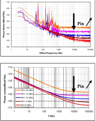
equivalently, the envelope technique) and simulation of the additive noise using the ADS nonlinear noise tools or, as an alternative, the measured nonlinear noise figure and equation (1), it is possible to reach a very good agreement between measured and simulated phase noise. Figure 6a and 6b represents such a comparison, for a SiGe bipolar
device maintained between two 50 Ω loads and
feed by a 3.5 GHz signal.
The device residual phase noise is measured using previously described techniques [5,8,10], which minimize the effect of the source noise (and particularly, of its AM noise). The relative increase of the phase noise floor at low carrier level is typical of an additive noise (equation (1)). The 1/f phase noise is almost constant at high power level, and increases at very low input power (-20 dBm). The phase noise is simulated from a device nonlinear model similar to the one described in paragraph III and using ADS and the above described two step simulation (a different technique for the additive and the multiplicative noise contributions). The simulated data fit well the measured data on the whole input power range.
With such a modelling approach, it is possible not only to predict an oscillator phase noise, but also to optimize the final result. The optimization of the amplifier is easier than the one of the oscillator, for already mentioned reasons (convergence). Moreover, some simple rules may help in designing a low phase noise oscillator with this technique. There is actually a trade-off to find between the gain requirements and the amplifier phase noise. It has been found in previous studies that matching a transistor for high gain performance results in a poor phase noise performance [9]. On the contrary, a resonator requires a sufficient decoupling to reach a high enough loaded Q factor
(QL). Finally, a 6 dB losses coupling (QL = Q0/2)
can be considered as an optimum coupling both for additive phase noise [11] or conversion phase noise [8] contributions, in a single stage amplifier oscillator. This means that the amplifier gain should be higher than 7 dB or, more realistically to take into account the circuit losses, 9 dB. This gain performance is easy to reach at moderate frequencies (up to 5 GHz, as an example), giving many possibilities to optimize the transistor phase noise versus RF loading, but is more difficult at higher frequencies without matching the device for maximum small signal gain (which again, is far of being an optimized load versus phase noise performance). Another important case is the one of sapphire oscillators, and particularly of cryogenic oscillators. In this case, the resonator is reached through long cables, in order to prevent it from being heated. These cables induce extra losses, and the use of an amplifier featuring a small signal gain of at least 14 dB becomes mandatory.
We found that, both for 10 GHz applications and for cryogenic 5 GHz to 7 GHz applications, it was impossible to get optimized results by keeping a single stage amplifier. Therefore, a low phase noise two stages amplifier has been studied.
-180 -170 -160 -150 -140 -130 -120 -110 1 10 100 1000 10000 100000 Offset frequency (Hz) P h a s e N o is e ( d B ra d ²/ H z ) -175 -165 -155 -145 -135 -125 -115 1 10 100 1000 10000 100000 f (Hz) P h a s e n o is e (d B ra d ²/ H z ) Pin=-20 dBm Pin=-15 dBm Pin=-10 dBm Pin=-5 dBm Pin=0 dBm
Figure 6 (6 a and 6b) : Measured (above, 6a) and
simulated (below, 6b) 3.5 GHz phase noise of a bipolar transistor (TB2) at different microwave input power levels ranging from -20 dBm up to 0 dBm.
-180 -170 -160 -150 -140 -130 -120 -110 1 10 100 1000 10000 100000 frequency (Hz) P h a s e N o is e ( d B c /H z ) Mesures à Pe=0 dBm Modèle en PI à Pe=0 dBm
Figure 7 :Phase noise simulation measurement
comparison at high power (0 dBm) ; TB2 at 3.5 GHz.
V. Two stages low phase noise
amplifier and cryogenic oscillator
simulation
Different combinations of the modeled devices have been studied in order to design a two stages amplifier. If two identical stages are considered, the overall phase noise should be increased of about 3 dB, if the phase noise of each stage is not too sensitive to the input power level.
Pin
This is probably true for the 1/f phase noise, as shown, as an example, in Figure 6. But this is not true for the additive noise floor, which improves relatively to the signal at high level. Finally, the phase noise of the two stages amplifier should be 3 dB higher than the one of the single stage amplifier in the 1/f region, and should be imposed by its first stage in the noise floor region.
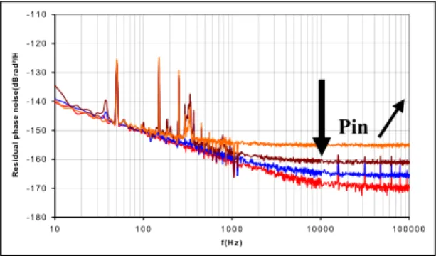
-1 8 0 -1 7 0 -1 6 0 -1 5 0 -1 4 0 -1 3 0 -1 2 0 -1 1 0 1 0 1 0 0 1 0 0 0 1 0 0 0 0 1 0 0 0 0 0 f(H z ) R e s id u a l p h a s e n o is e (d B ra d ²/ H
Figure 8 :3.5 GHz measured residual phase noise of
two cascaded TB2, maintained onto 50 Ω load (Pin =-15 dBm,-10 dBm, -5dBm and 0 dBm).
The measured phase noise of such an amplifier, realized with two TB2 devices, is depicted in Figure 8, for different input power levels. The measured phase noise is very close to the one of the single stage device (Figure 6), and is mainly imposed in the case of this transistor by the first stage (both 1/f and additive phase noises are improved at high power).
Therefore, we have chosen this approach to design a low phase noise two stages amplifier for cryogenic applications. The gain-phase noise trade-off is analysed and optimized on each stage, using a single stub approach such as in previous one stage amplifier design [8]. The transistors are biased for low 1/f noise i.e. using a low impedance bias network on the transistors bases [8]. The complete circuit is still not yet available, but the oscillator simulated results are very promising, as shown in Figure 9. This final simulation has been performed on ADS, using the oscillator phase noise dedicated tools of this software.
avec A=10 L=6 Qo=2 000 000
-180 -170 -160 -150 -140 -130 -120 -110 -100 -90 -80 1 10 100 1000 10000 100000 1000000 f(Hz) B ru it d e p h a s e (d B c /H z )
Figure 9 : Simulated phase noise of an oscillator
with a two stages TB1 amplifier and cryogenic sapphire resonator @ 5 GHz (Ic = 10mA, Vce =2V)
Conclusion
A modelling technique, dedicated to microwave amplifier phase noise calculation, has been presented. This technique takes into account the two main noise contributors to phase noise in silicon bipolar transistor amplifiers: the 1/f converted low frequency noise and the additive high frequency noise. CAD calculation of each noise type is presented, taking into account the nonlinear effects which change both the device low frequency noise and the device high frequency noise figure when it is pushed into compression. This model compares well to the experiment on various single stage microwave amplifiers. It is also used to optimise a two stages amplifier dedicated to cryogenic sapphire oscillator applications. Preliminary simulated results for this oscillator are given.
References
[1] D.B. Leeson, "A simple model of feedback oscillator noise spectrum," Proc. Letters of IEEE, Vol. 54, N° 2, pp. 329-330, 1966.
[2] O. Llopis, et al, "Low level and reflection phase noise measurements," IEE Electron. Lett., Vol. 37, N° 2, pp. 126-129, 2001.
[3] O. Llopis, et al, "Nonlinear noise modelling of a PHEMT device through residual phase noise and low frequency noise measurements," Proc. of the IEEE MTT Symposium, pp. 831-834, May 2001
[4] G. Massobrio, P. Antognetti, Semiconductor Device Modelling with SPICE McGraw-Hill Ed.
[5] G. Cibiel, L. Escotte, O. Llopis, A study of the correlation between HF noise and phase noise in low noise silicon based transistors , IEEE Transactions on Microwave Theory and Tech., vol 52, n° 1, Janvier 2004, pp. 183-190.
[6] F. Bonani et al. Noise source modelling for cyclostationary noise analysis in large signal device operation , IEEE Trans. on Electron. Dev., n° 9, sept 2002, pp. 1640-1647.
[7] H.J. Siweris, B. Schiek, "A GaAs FET oscillator noise model with a periodically driven noise source", 1986 EuMC Proceedings, pp. 681-686.
[8] G. Cibiel, et al, "Optimization of an ultra low phase noise sapphire - SiGe HBT oscillator using nonlinear CAD", IEEE Transactions on Ultrasonics, Ferroelectrics, and Frequency Control, Vol. 51, No. 1, pp. 33-41, January 2004.
[9] M. Regis, O. Llopis, J. Graffeuil, "Nonlinear modeling and design of bipolar transistors ultra low phase noise dielectric resonator oscillators" IEEE Trans. on MTT, Vol. 46, N° 10, pp. 1589-1593, October 1998.
[10] G. Cibiel, et al, "AM noise impact in low level phase
noise measurements," IEEE Trans. on UFFC, Vol. 49, N° 6, pp. 784-788, 2002.
[11] J. K. A. Everard, "Low noise oscillators" Proc. of
the IEEE MTT-Symposium, pp. 1077-1080, 1992.