DESIGN AND IMPLEMENTATION OF INTEGRATED HIGH EFFICIENCY LOW-VOLTAGE CMOS DC-DC CONVERTERS
OMAR AL-TERKAWI HASIB
D´EPARTEMENT DE G ´ENIE ´ELECTRIQUE ´
ECOLE POLYTECHNIQUE DE MONTR ´EAL
M ´EMOIRE PR´ESENT ´E EN VUE DE L’OBTENTION DU DIPL ˆOME DE MAˆITRISE `ES SCIENCES APPLIQU ´EES
(G ´ENIE ´ELECTRIQUE) D´ECEMBRE 2010
´
ECOLE POLYTECHNIQUE DE MONTR´EAL
Ce m´emoire intitul´e :
DESIGN AND IMPLEMENTATION OF INTEGRATED HIGH EFFICIENCY LOW-VOLTAGE CMOS DC-DC CONVERTERS
pr´esent´e par : M. AL-TERKAWI HASIB Omar
en vue de l’obtention du diplˆome de : Maˆıtrise `es Sciences Appliqu´ees a ´et´e dˆument accept´e par le jury constitu´e de :
M. AUDET Yves, Ph.D., pr´esident
M. SAWAN Mohamad, Ph.D., membre et directeur de recherche M. SAVARIA Yvon, Ph.D., membre et co-directeur de recherche M. ZHU Guchuan, Doct., membre
To my dear mother, I can’t be grateful enough. . .
Acknowledgments
Writing this part of the thesis might prove to be a very difficult task for me. To include all the people who are responsible for me being here in few lines is almost impossible. First, I would like to thank God the Merciful for providing me with such a wonderful opportunity, surrounding me with an amazing group of people and keeping me in a good health and well-being. Among those amazing people are my parents who raised me to never quit and to keep learning and to pursue my dreams with all my heart. I am especially grateful to my mother who loved me and supported me unconditionally during all these years. Thank you Mom! I also thank the rest of my family for their continuous love, support and encouragements.
I would not be writing this thesis if it weren’t for my inspiring professors. I would like to start by thanking my current director Prof. Mohamad Sawan for accepting me as his student and giving me the chance to purse my master’s degree. His guidance and support are greatly appreciated. I would also like to thank my co-director Prof. Yvon Savaria for the time and effort he put in helping me complete this work and for tolerating my mistakes and the ridiculous amount of typos that I make. I’m also grateful for the teaching and encouragement I received from my undergraduate professors, especially Prof. Mohamed Zribi and Dr. Nabil Khachab.
I appreciated the kindness that I’ve seen from the people in my research group (Polystim). A special thank to Fay¸cal Mounaim who has been a great lab mate and friend during the two past years. His help and experience was invaluable in completing this work. My gratitude also goes to S´ebastien Ethier and Guillaume Simard for sharing their experience and knowledge with me. I would also like to extend my thanks to our technical support R´ejean Lepage and our secretary Marie-Yannick Laplante.
I would like to thank all of my friends. Each of them have contributed in building my current personality. I start by thanking Ahmad Haider for pushing me to apply to ´Ecole Polytechnique de Montr´eal despite my poor knowledge in French. I would like to thank Omar Al-Naggar for teaching me how to be systematic in learning and presenting my ideas. My thanks goes to Ali-Akbar Samadani, Khadige Abboud and their family for opening the door to both their hearts and homes for me. I’m also grateful to the group of friends who organized a welcoming party each time I visited Kuwait and to the people who sent me encouragement emails during difficult times. More importantly, I would like to thank Ali
Al-Naggar, Mohamad Adly, Ahmad Boland and Afrah Lutfi for supporting me and for being my good friends.
Finally, I would like to acknowledge the financial support from the Natural Sciences and Engineering Research Council of Canada (NSERC), the Resmiq research network supported by the Fonds Qu´ebecois de la Recherche sur la Nature et les Technologies, and the products and services provided by CMC Microsystems that facilitated this research, including CAD tools and fabrication services.
R´
esum´
e
De nos jours, les appareils portatifs sont utilis´es dans plusieurs applications. Ils utilisent en g´en´eral une batterie qui doit ˆetre remplac´ee ou recharg´ee r´eguli`erement. Dans le cas d’appli-cations biom´edicales, la dur´ee de vie de la batterie est un param`etre critique. Pour un appareil implantable, une longue dur´ee de vie est un objectif primordial. Cet objectif est g´en´eralement atteint en r´eduisant la consommation de puissance des circuits constituant l’implant. Parmi les diverses techniques existantes qui permettent la r´eduction de la consommation en puis-sance des circuits CMOS, on retrouve la technique d’ajustement dynamique de la tension (dynamic voltage scaling - DVS). En r´eduisant la tension d’alimentation, la consommation totale des circuits peut ˆetre diminu´ee. Cependant cette technique ne peut ˆetre impl´ement´ee sans faire appel `a des circuit d´edi´es `a une gestion intelligente de l’´energie. Dans ce contexte, l’utilisation de convertisseurs de tension DC-DC devient n´ecessaire pour ´economiser la charge de la batterie. Mais pour garantir une r´eduction effective de la consommation globale, des convertisseurs DC-DC de haute efficacit´e doivent ˆetre utilis´es. A cette contrainte se rajoute la miniaturisation en utilisant des circuits hautement int´egr´es pour les applications telles que les implants biom´edicaux. Le d´efi r´eside dans la conception d’un convertisseur DC-DC totalement int´egr´e tout en assurant une haute efficacit´e sur une grande plage de tension de sortie. De plus, les appareils tels que les implants ´electroniques fonctionnet souvent en mode de veille pour r´eduire la consommation, entrainant ainsi des variations cons´equentes de la charge du convertisseur DC-DC. Ceci rajoute un d´efi suppl´ementaire pour le maintient d’une haute efficacit´e de la conversion DC-DC `a faible charge.
Dans ce m´emoire, nous pr´esentons la conception d´etaill´ee d’un convertisseur DC-DC haute-ment efficace et totalehaute-ment int´egr´e dans une technologie CMOS `a faible tension. Nous pro-posons une impl´ementation originale et totalement int´egr´ee d’un convertisseur DC-DC `a ca-pacit´es commut´es (switched capacitor - SC) op´erant avec un contrˆole asynchrone. L’efficacit´e du convertisseur est maintenue ´elev´ee en ajustant sa topologie et sa fr´equence d’op´eration selon la charge. Le convertisseur SC DC-DC propos´e utilise trois topologies distinctes pour r´ealiser trois taux de conversion diff´erents. Ainsi, le convertisseur maintient une haute effi-cacit´e `a diff´erents niveaux de tensions de sortie. De plus, afin de r´eduire les pertes d’´energie, le contrˆole asynchrone adapte la fr´equence d’op´eration aux diverses conditions de charge. Ce contrˆole est ´egalement capable d’adapter la taille des interrupteurs du convertisseur SC DC-DC pour am´eliorer encore plus l’efficacit´e de la conversion. Les r´esultats exp´erimentaux de ce travail confirment la th´eorie et les simulations conduites lors de la conception. Une puce
de 1.5× 1.5mm2 contenant le convertisseur propos´e a ´et´e fabriqu´e en utilisant la technolo-gie IBM CMOS 0.13µm. Le convertisseur est capable d’atteindre une efficacit´e maximale de 80% en fournissant une tension de sortie entre 0.3V et 1.1V `a partir d’une entr´ee `a 1.2V . Le convertisseur utilise un ensemble de condensateurs int´egr´e dont la capacit´e totale est de 350pF pour fournir une puissance de sortie maximale de 230µW , ciblant ainsi de nombreuses applications `a tr`es faible puissance.
Abstract
Today, battery-powered portable devices are used in many applications. In applications like biomedical implants, the battery life is a major concern. Since replacing the battery of an implant needs a surgical procedure, a long battery life is a goal that all implants try to achieve. This is normally done by reducing the power dissipation in the implant’s circuitry. One of the various techniques that exist for reducing the power consumption in CMOS circuitry is the dynamic voltage scaling (DVS) technique. By reducing the supply voltage, the overall power consumption of the circuits can be decreased. This technique cannot be implemented without power management blocks. The use of DC-DC converters becomes a must to save battery power. The overall power reduction can be improved by introducing high efficiency DC-DC converters. Moreover, to provide patients with the most comfort, small integrated circuits should be used in applications such as biomedical implants.
The challenging aspect of designing integrated DC-DC converters is keeping the efficiency high while providing an adjustable output voltage. Additionally, devices such as electronic implants go in and out of stand-by mode to reduce power consumption. From the perspective of the DC-DC converter, the output load power is varying according to the mode of operation of the implant. This adds another challenge of sustaining the DC-DC conversion efficiency high under various loading conditions. At very light loads, preserving a high conversion efficiency is a challenge.
In this master thesis, a detailed design of a high-efficiency low-voltage fully integrated DC-DC converter is presented. A unique structure of a fully integrated switched-capacitor (SC) DC-DC converter with asynchronous control is proposed. The efficiency of the converter is maintained high by adjusting the converter topology and operating frequency according to the loading conditions. The proposed SC DC-DC converter uses three different topologies to achieve three different conversion ratios. By doing so, the converter maintains high conversion efficiency at various output voltage levels. Also, an adaptive operating frequency is used by the asynchronous control to reduce efficiency losses at various loading conditions. Moreover, the applied control is able to change the size of the switches in the SC DC-DC converter when needed. This leads to further enhancement in the overall conversion efficiency. The simulations and experimental results of this work supported the theories of the design. The converter was fabricated on a 1.5 × 1.5mm2 chip using IBM CMOS 0.13µm technology.
output voltages between 1.1V and 0.3V with a maximum efficiency of 80%. This design is aimed at ultra-low-power applications. It uses a total of 350pF on-chip capacitors to support a maximum output power of 230µW .
Condens´
e en fran¸
cais
1. Introduction
Au cours de la derni`ere d´ecennie, la demande d’appareils portatifs a connu une augmenta-tion constante. Grˆace `a la miniaturisation, aux multiples fonctionnalit´es et `a la possibilit´e de les alimenter par batterie uniquement, ces appareils ont trouv´e leur place dans de nombreuses applications y compris les implants biom´edicaux. Dans de tels syst`emes, la dur´ee de vie de la batterie est un facteur crucial [35]. Il est donc n´ecessaire d’augmenter la dur´ee de vie de la batterie et cela passe par la r´eduction autant que possible de la dissipation de puissance des composants ´electroniques.
L’ajustement dynamique de la tension (DVS) constitue la principale technique utilis´ee pour r´eduire la consommation d’´energie des circuits CMOS [47]. Celle-ci exploite le fait que la consommation d’´energie est reli´ee de mani`ere quadratique `a la tension d’alimentation (´equation 1.1). Pour tirer avantage de la technique DVS, des convertisseurs DC-DC abaisseurs de tension qui peuvent fournir des sorties variables sont requis [10, 19, 26, 29, 30, 40]. De plus, il a ´et´e d´emontr´e que la technique DVS utilis´ee dans un syst`eme asynchrone peut r´eduire encore plus la consommation de puissance des circuits utilis´es [24].
L’objectif de ce travail est de concevoir un convertisseur DC-DC hautement efficace, totale-ment int´egr´e et d´edi´e aux implants biom´edicaux. Le type de convertisseur DC-DC propos´e est `a capacit´es commut´ees (switched capacitor- SC) avec un taux de conversion variable. Ce type de convertisseurs convient aux implants biom´edicaux car il est efficace et peut ˆetre compl`etement int´egr´e sur puce [29, 43]. Pour ˆetre capable d’appliquer la technique DVS, le convertisseur SC DC-DC doit varier la tension de sortie. Cependant, l’efficacit´e de conver-sion maximale que le convertisseur SC DC-DC puisse fournir d´epend de la tension de sortie (´equation 2.5). Heureusement, ce probl`eme peut ˆetre r´esolu en ajustant le taux de conver-sion du SC DC-DC en fonction de la tenconver-sion de sortie requise. Il existe diff´erents types de pertes d’´energie qui contribuent `a la r´eduction de l’efficacit´e (´equation 2.8). L’une des princi-pales pertes d’´energie est due aux commutations (Esw). Ces pertes d´ependent de la fr´equence
de commutation. Afin de r´eduire ces pertes, le convertisseur SC DC-DC devrait commuter seulement quand c’est n´ecessaire. Or, un convertisseur SC DC-DC d´epend en g´en´eral d’une fr´equence d’horloge constante. La puissance de sortie, l’efficacit´e de la conversion ainsi que le choix de la taille des condensateurs et des commutateurs au moment de la conception
d´ependent de la fr´equence de cette horloge.
La recherche d’une fr´equence d’op´eration optimale qui maximiserait l’efficacit´e par rapport `
a la taille des condensateurs et des commutateurs peut ˆetre laborieuse. Ceci devient encore plus complexe quand le convertisseur SC utilise diff´erentes topologies `a diff´erentes tensions de sortie. La conception pr´esent´ee ici utilise un contrˆoleur totalement asynchrone qui varie la fr´equence selon la topologie utilis´ee et selon le courant requis par la charge du convertisseur DC-DC. Le contrˆoleur r´eduit la commutation au minimum n´ecessaire et r´eduit ainsi les pertes de puissance associ´ees `a la commutation. De plus, afin de pouvoir op´erer sur une large plage de tension de sortie tout en maintenant une bonne efficacit´e, le convertisseur SC DC-DC propos´e bascule entre trois diff´erentes topologies permettant les taux de conversions suivants : 1,23 et
1 3.
2. Conception du convertisseur SC DC-DC propos´
e
2.1 Vue d’ensemble de la structure propos´
ee
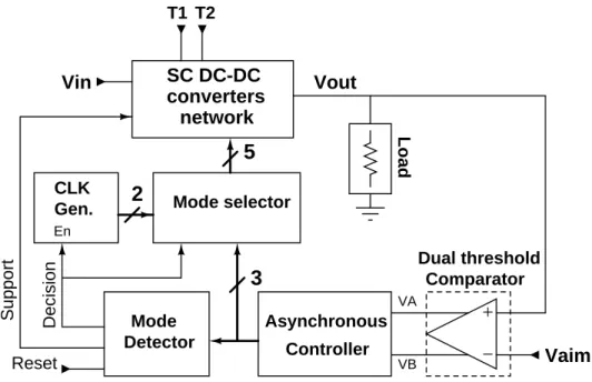
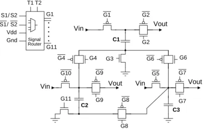
Un aper¸cu complet de la structure propos´ee est illustr´e `a la Fig. 3.1. Le r´eseau du conver-tisseur (SC DC-DC converters network) a la possibilit´e de changer sa topologie en fonction des signaux num´eriques T1 et T2. Les taux de conversion qui peuvent ˆetre r´ealis´es par les
topologies possibles sont 1, 23 et 13. La quatri`eme combinaison de T1 et T2 d´esactive le
conver-tisseur. La boucle de r´etroaction est constitu´ee d’un comparateur `a deux tensions de seuil, d’un contrˆoleur asynchrone (Asynchronous Controller), d’un d´etecteur de mode (Mode De-tector) et d’un s´electeur de mode (Mode Selector). Le comparateur g´en`ere deux signaux num´eriques, VA et VB. VA est le r´esultat de la comparaison entre Vout et Vaim, alors que VB
est g´en´er´e par un seuil inf´erieur `a Vaim de pr`es de 0.1V. La combinaison de VA et de VB cr´ee
trois valeurs d’entr´ee possibles utilis´ees par le contrˆoleur asynchrone.
Le contrˆoleur asynchrone propos´e g´en`ere trois signaux dont les largeurs d’impulsion et les fr´equences sont ajust´ees en fonction de la charge. Ces signaux de commande sont transmis au r´eseau du convertisseur SC DC-DC par l’interm´ediaire du s´electeur de mode, qui choisit entre deux modes d’op´eration : soit le mode asynchrone (Asynchronous Drive Mode) qui est le principal mode de fonctionnement, soit le mode synchrone (Synchronous Drive Mode) qui est un mode de repli disponible lorsque la charge d´epasse la valeur attendue. En mode asynchrone, les signaux du contrˆoleur sont transmis au r´eseau du convertisseurs SC DC-DC, tandis que dans le mode synchrone, les signaux sont transmis `a partir d’un g´en´erateur d’horloge.
Le s´electeur de mode choisit un signal pour piloter le r´eseau du convertisseurs en se basant sur le signal ”Decision” issu du d´etecteur de mode. Pour des valeurs de charge r´eguli`eres, le signal Decision est au niveau bas, ce qui d´esactive le g´en´erateur d’horloge et transmet les signaux du contrˆoleur asynchrone vers le r´eseau du convertisseurs SC DC-DC. Quand la charge de courant d´epasse la capacit´e nominale du r´eseau de convertisseurs, le signal Decision passe au niveau haut et configure le convertisseur `a un circuit synchrone en activant une horloge `a 4 MHz pour op´erer le convertisseur. La raison principale pour basculer vers le mode synchrone est de maintenir l’ondulation de la tension de sortie faible dans le cas de grands courants de charge. Ceci sera expliqu´e dans la section suivante.
Selon la taille des condensateurs et des commutateurs utilis´es ainsi que la topologie choisie, il y a une limite de courant qui peut ˆetre d´elivr´e `a la charge. Le d´etecteur de mode est le bloc qui d´etecte quand la limite de courant du r´eseau de convertisseurs est d´epass´ee. Le processus de d´etection se fait par l’inspection du motif des signaux g´en´er´es par le contrˆoleur asynchrone. Une fois que le motif r´egulier change, le d´etecteur de mode envoie le signal ”Support” au r´eseau de convertisseurs. Ce signal active des commutateurs suppl´ementaires parall`eles dans le convertisseur. Ce faisant, le convertisseur augmente la limite maximale du courant de charge d’une certaine valeur. Si cela s’av`ere insuffisant pour alimenter la charge, alors le d´etecteur passe le signal Decision au niveau haut mettant ainsi le convertisseur en mode synchrone.
2.2 Strat´
egie de contrˆ
ole asynchrone
Le r´eseau de convertisseurs dans la structure pr´esent´ee pr´ec´edemment est constitu´e d’un commutateur direct et de deux convertisseurs SC DC-DC `a topologie ajustable (Fig. 3.2). Le commutateur direct est utilis´e pour initialiser la capacit´e de charge `a la tension d´esir´ee, et les convertisseurs SC DC-DC gardent Vout `a cette valeur. Cette op´eration donne au convertisseur non seulement un temps de mont´ee rapide lors du basculement entre les topologies mais ´
egalement une conversion efficace en r´egime permanent. Chacun des convertisseurs SC DC-DC est compos´e de trois condensateurs et de onze interrupteurs (Fig. 3.3). Selon les topologies utilis´ees, les interrupteurs sont r´egl´es sur ON ou OFF, sous contrˆole d’un signal ou de son compl´ement (voir le tableau 4.3). L’arrangement illustr´e dans la Fig. 3.3 peut connecter les condensateurs dans quatre diff´erentes combinaisons s´erie-parall`ele qui permettent trois taux de conversion possibles (1, 23 et 13).
Le contrˆoleur asynchrone est en r´ealit´e une machine `a ´etats asynchrone. Pour piloter le r´eseau de convertisseurs SC DC-DC de mani`ere asynchrone, le contrˆoleur attend certains
´
ev´enements qui sont d´eclench´es par la tension de sortie. Ces ´ev´enements sont d´etect´es par le comparateur qui compare Vout `a deux seuils VAref et VBref. Dans le circuit propos´e, VAref
= Vaim, VBref = Vaim− 0.1V et Vaim est la tension de sortie d´esir´ee. De ces deux seuils, VA
et VB sont g´en´er´es par le comparateur. Le diagramme d’´etats qui d´efinit la g´en´eration des
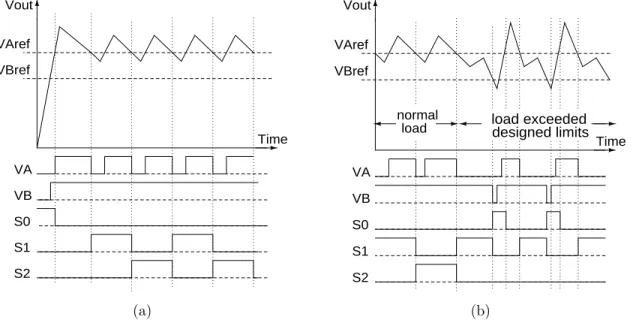
signaux de contrˆole S0, S1 et S2 par rapport `a VA et VB est montr´e dans la Fig. 3.6. Le circuit
complet du contrˆoleur asynchrone est donn´e sur la Fig. 4.2.
Lorsque le circuit d´emarre pour la premi`ere fois, le contrˆoleur d´etecte que Vout est inf´erieur aux deux seuils puis fournit les signaux de commande de mani`ere `a ce que la capacit´e de charge ainsi que les deux convertisseurs SC commencent `a se charger. Aussitˆot que la tension de sortie d´epasse VAref, le contrˆoleur d´esactive le commutateur direct. La diff´erence entre la
constante de temps du m´ecanisme de charge RC et le retard dans la boucle de r´etroaction entraine des d´epassements de tension de sortie. Ensuite, le contrˆoleur va attendre que la tension de sortie descende en dessous de VAref pour connecter l’un des convertisseurs SC `a
la charge. Dans des conditions normales de charge, la charge stock´ee par le convertisseur va relever la tension au del`a de VAref. Le convertisseur connect´e fournira la tension de sortie
n´ecessaire jusqu’`a ce que toutes les charges disponibles soient consomm´ees. Lorsque la tension de sortie redescend en dessous de VAref, le contrˆoleur connecte la sortie `a l’autre convertisseur
SC pendant que le pr´ec´edent se recharge. A partir de l`a, le contrˆoleur continuera d’alterner les deux convertisseurs pour alimenter la charge. La Fig. 3.5(a) montre un chronogramme qui r´esume cette op´eration de contrˆole en fonction de la tension de sortie.
Quand la charge devient sup´erieure `a la valeur attendue, le convertisseur SC DC-DC ne sera pas en mesure d’´elever Vout au dessus de VAref avant que la charge stock´ee soit consomm´ee.
La tension Vout commencera alors `a baisser jusqu’`a ce qu’elle atteigne VBref (Fig. 3.5(b)). `A
ce moment l`a, le contrˆoleur asynchrone activera l’interrupteur direct pour ´elever la tension de sortie. Cela remettra `a z´ero l’op´eration du contrˆoleur et ce dernier essayera de soutenir la charge de nouveau avec les convertisseurs. Si la charge reste ´elev´ee pendant un certain temps, le d´etecteur de mode activera des interrupteurs de sortie additionnels. Dans le cas o`u cela ne r´esoud pas le probl`eme, le d´etecteur de mode d´ecidera de passer au mode synchrone pour parvenir `a une meilleure r´egulation.
2.3 D´
etecteur de Mode et S´
electeur de Mode
Le bloc qui est charg´e de d´eterminer si les convertisseurs SC sont en mesure de supporter la charge ou pas, est le d´etecteur de mode. Il peut indirectement d´eterminer si le courant de charge d´epasse les capacit´es des convertisseurs SC en inspectant le motif du signal de
commande g´en´er´e par le contrˆoleur asynchrone. Comme vu pr´ec´edemment sur la Fig. 3.5(b), le motif des signaux de commande S0, S1 et S2 change quand le convertisseur SC ne peut
pas supporter la charge.
Le d´etecteur de mode illustr´e sur la Fig. 3.7 est con¸cu pour d´etecter ce motif. Initialement, le d´etecteur de mode est remis `a z´ero. Cela implique que toutes les bascules du circuit sont remise `a zero et les signaux Support et Decision sont au niveau bas. Quand le d´etecteur de mode est activ´e, il d´esactivera tous les transistors de remise `a z´ero et activera M2, M7, M11
et M16. Le motif normal d´ebutera avec le passage `a ’1’ de S1 alors que S0 et S2 sont `a ’0’. S1
activera le transistor M3 qui tire le courant de cette branche et bascule l’´etat de Latch1 pour
appliquer finalement un niveau haut sur la grille de M9.
Maintenant M9 est activ´e et il y a deux sc´enarios possibles : soit S2 passe `a ’1’ alors que
S1 passe `a ’0’ (cas normal), soit S0 passe `a ’1’ et S1 passe `a ’0’ (si le courant de charge a
d´epass´e la limite). Dans le premier cas, M5 sera activ´e et remettra Latch1 `a son ´etat initial
qui d´esactive M9. Alors que S1 et S2 s’alternent, Latch1 continuera `a changer d’´etat et le
signal Support restera bas. Dans le second cas, M8 sera activ´e et basculera l’´etat de Latch2,
passant le noeud X1 au niveau haut. Pour ´eviter des erreurs dans le processus de d´etection,
les portes NAND coupl´ees par croisement garantiront que S1 a compl`etement atteint z´ero
avant de changer le signal Support `a ’1’.
Une fois que le signal Support est haut, des commutateurs suppl´ementaires dans les conver-tisseurs sont activ´es pour supporter le courant de charge ´elev´ee. Si cela n’´etait pas suffisant pour supporter la charge, le motif des signaux de commande sera r´ep´et´e. Le bloc B dans le d´etecteur de mode d´etectera la r´ep´etition du motif et d´elivrera le signal Decision. Lorsque le signal Decision est haut, le s´electeur de mode va basculer vers le mode synchrone. Fig. 4.4 montre le circuit du s´electeur de mode. La transition entre les deux modes d’op´eration ainsi que les signaux de commande du contrˆoleur asynchrone et du d´etecteur de mode sont montr´es dans la Fig. 4.7.
2.4 Comparateur `
a double seuils
Le comparateur qui a ´et´e utilis´e pour ce convertisseur est montr´e sur la Fig. 4.5. Pour r´eduir la consommation d’´energie et la surface de silicium, nous avons con¸cu un compara-teur `a deux seuils plutˆot que d’utiliser deux comparateurs. Ce comparateur est bas´e sur un amplificateur op´erationnel `a transconductance (OTA) et des miroirs de courant. Ceci a ´et´e inspir´e du travail accompli par [16].
Le comparateur fonctionne comme suit. M8 est utilis´e pour polariser le comparateur. La
paire diff´erentielle M6-M7 permettra de comparer la tension de sortie Vout du convertisseur
DC-DC avec Vref qui est la tension d´esir´ee. Le r´esultat de la comparaison r´esultera en un courant dans l’une des branches de la paire diff´erentielle. Le courant est ensuite achemin´e `a M2 et M10. La diff´erence entre les courants de drains de M2 et M10 va tirer VA∗ soit vers Vdd
(1.2V ) soit vers la masse. Les transistors M2 et M10 sont de dimensions telles que VA∗ = 0.6
lorsque Vout= Vaim. En changeant la taille des transistors de sortie, le seuil peut ˆetre d´eplac´e.
M1 et M9 sont dimensionn´es de sorte que VB∗ est g´en´er´e `a un seuil inf´erieur `a VA∗ de 60mV .
Pour g´en´erer VA et VB qui d´eclenchent le contrˆoleur asynchrone, VA∗ et VB∗ sont amplifi´es par
des inverseurs.
La Fig. 4.6 pr´esente les r´esultats des analyses de simulation DC du comparateur montr´e sur la Fig. 4.5. Le balayage est fait avec Vbias = 0.2V et Vaim = 0.6V . Les r´esultats sur
la Fig. 4.6(a) montrent la g´en´eration de VA∗ et VB∗. Le seuil sup´erieur peut ˆetre mesur´e `a 599.2mV alors que le seuil inf´erieur est de 541.1mV . Quant `a la consommation de puissance, ce comparateur ne consomme que 2.4µW au maximum qui se produit lorsque Vout = Vaim.
Fig. 4.6(b) montre le courant dans chaque branche du comparateur, ainsi que le courant total consomm´e.
3. R´
esultats
La conception pr´esent´ee dans ce m´emoire a ´et´e impl´ement´ee dans l’environnement Ca-dence avec la technologie CMOS 0.13µm de IBM. La structure compl`ete, except´e le g´en´erateur d’horloge, a ´et´e int´egr´ee et une puce a ´et´e fabriqu´ee. Fig. 3.8 montre une vue microscopique de la puce r´esultante. La superficie totale incluant les pads est de 2.225mm2 mais seulement
0.52mm2 de cette superficie est effectivement occup´ee par les circuit actifs. Celle-ci utilise des
capacit´es int´egr´es MIM de 150pF pour chaque convertisseur, plus 50pF pour le condensateur de sortie. Le courant maximum qui peut ˆetre fourni est de 240µA. Ceci peut ˆetre facilement augment´e en augmentant la taille des condensateurs utilis´es. Le convertisseur fonctionne sur une alimentation de 1.2V et peut fournir des tensions de sortie de 300mV `a 1.1V .
Les Fig. 3.9 et 4.11 montrent la r´egulation de la tension de sortie `a des valeurs diff´erentes. D’autre part, Fig. 3.10 et 4.8-4.10 montrent l’efficacit´e du convertisseur sous diff´erentes topologies, diff´erents courants de charge et diff´erentes tensions de sortie. Dans les derni`eres figures, l’efficacit´e a ´et´e s´epar´ee en trois courbes nous permettant de voir la contribution des pertes li´ees aux composants parasites, celles dues `a la commutation et `a la conduction.
Les courbes d’efficacit´e pr´esent´ee sont d´efinies dans les ´equations (3.3-3.5). De plus, dans ces figures les courbes d’efficacit´e avec et sans les pertes de commutation sont presque parall`eles, impliquant que celles-ci diminuent quand le courant de charge est r´eduit. En outre, `a faible charge, les pertes dans les composants parasites et les fuites de courant r´eduisent l’efficacit´e de mani`ere drastique. Enfin, la comparaison avec les r´ecents travaux effectu´es sur les con-vertisseurs SC DC-DC montre que nous avons r´eussi `a obtenir de bons r´esultats lorsque le convertisseur est command´e de mani`ere asynchrone (tableau 3.1).
4. Conclusion
L’importance de la dur´ee de vie de la batterie pour les appareils portatifs et les implants biom´edicaux a conduit les chercheurs `a d´evelopper de nouvelles m´ethodes de r´eduction de la consommation de puissance. L’ajustement dynamique de la tension (DVS) est l’une des m´ethodes les plus connues pour r´eduire la consommation de puissance des circuits CMOS. Pour appliquer cette technique, des convertisseurs DC-DC `a tension de sortie ajustable sont utilis´es. `A cette fin, nous avons con¸cu un convertisseur DC-DC qui serait appropri´e pour de telles applications.
Dans ce m´emoire, nous avons con¸cu et d´emontr´e un convertisseur SC DC-DC hautement ef-ficace et totalement int´egr´e dans une structure capable de supporter des syst`emes `a tr`es faible consommation d’´energie grˆace `a une tension de sortie ajustable et un fonctionnement asyn-chrone. Pour ce convertisseur, nous avons adopt´e une strat´egie asynchrone pour minimiser les pertes d’´energie dues `a la commutation et les pertes dynamiques des circuits logiques en adaptant la fr´equence d’op´eration aux conditions de charge. En se basant sur la strat´egie propos´ee de commande asynchrone, un processus de d´etection intelligent a ´et´e d´evelopp´e pour ajuster la taille des interrupteurs utilis´es selon la puissance de sortie. En outre, un mode de repli synchrone a ´et´e incorpor´e pour rendre le convertisseur robuste en pr´esence de conditions de charge inattendues. Enfin, les th´eories adopt´ees et les circuits con¸cus ont ´et´e v´erifi´es par des mesures exp´erimentales. Les r´esultats obtenus s’av`erent comp´etitifs avec les travaux r´ecents dans ce domaine.
Table of Contents
Dedication . . . iii Acknowledgments . . . iv R´esum´e . . . vi Abstract . . . viii Condens´e en fran¸cais . . . xTable of Contents . . . xvii
List of Tables . . . xx
List of Figures . . . xxi
List of Appendices . . . xxiv
List of Abbreviations and Symbols . . . xxv
Chapitre 1 Introduction . . . 1
1.1 Motivation . . . 1
1.2 Objectives and Challenges . . . 3
1.3 Contributions . . . 5
1.4 Thesis Organization . . . 5
Chapitre 2 Basic Switched-Capacitor Converters Principals And Literature Review . 7 2.1 SC DC-DC Converters Fundamentals . . . 7
2.1.1 Conversion Mechanism and the Conversion Ratio . . . 7
2.1.2 Efficiency of SC DC-DC converters . . . 9
2.1.3 Drive Signal Requirements . . . 12
2.2 SC DC-DC Converters Control Methods . . . 12
2.2.1 Open Loop Control . . . 13
2.2.2 Pulse Width Modulation (PWM) Control . . . 14
2.2.3 Pulse Frequency Modulation (PFM) Control . . . 14
2.4 Asynchronous Sequential Logic . . . 19
2.4.1 An Overview . . . 19
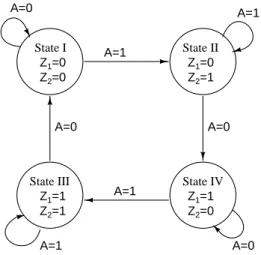
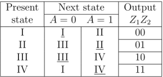
2.4.2 An Example of a 2-bit Counter . . . 21
2.4.3 Summary . . . 23
Chapitre 3 A Low-Power Asynchronous Step-Down DC-DC Converter for Implantable Devices . . . 24
3.1 Abstract . . . 24
3.2 Introduction . . . 25
3.3 Efficiency and Conversion Ratio . . . 26
3.4 Proposed DC-DC Converter . . . 28
3.4.1 Structure overview of the converter circuit . . . 28
3.4.2 Asynchronous Control strategy . . . 31
3.4.3 Load limits detection and operation mode selection . . . 34
3.5 Experimental Results . . . 36
3.5.1 Discussion . . . 40
3.5.2 Comparison with the latest reported results . . . 42
3.6 Conclusion . . . 43
Chapitre 4 Additional Circuits and Results . . . 45
4.1 Asynchronous Controller Circuit . . . 45
4.1.1 Synthesis of the Asynchronous Controller . . . 45
4.2 Signal Router Circuits . . . 47
4.3 Mode Selector Circuits . . . 49
4.4 Dual-Threshold Comparator Design . . . 50
4.5 Additional Measurement Results . . . 52
4.5.1 Transition Between Driving Modes . . . 52
4.5.2 Additional Efficiency Results . . . 53
4.5.3 Additional Output Voltage Measurements . . . 55
4.5.4 Output Ripple Measurements . . . 56
4.6 Layout Precautions and Recommendations . . . 57
4.6.1 Layout Protective Structures . . . 57
Chapitre 5 General Discussion . . . 60
Chapitre 6 Conclusion . . . 63
6.2 Limitations and Future Improvements . . . 64 References . . . 66 Appendices . . . 70
List of Tables
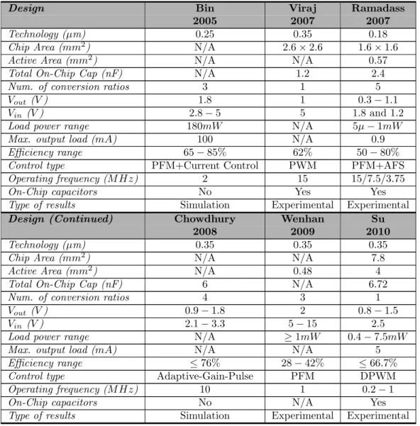
Table 2.1 Comparison of recent literature on step-down SC DC-DC converters . 18
Table 2.3 2-bit counter flow table. . . 22
Table 2.4 2-bit counter excitation table. . . 22
Table 3.1 comparison with recently published results . . . 42
Table 4.1 Asynchronous Controller flow table. . . 46
Table 4.2 Asynchronous Controller excitation table. . . 46
Table 4.3 The signal router’s output for each switch in the SC netwrok according to the conversion ratio needed (set by T1 and T2). φ is one of the drive signals, either S1 or S2 in the Asynchronous Drive Mode, or the clock signals (CLK and CLK) in the Synchronous Drive Mode. . . . 49
List of Figures
Figure 1.1 The SC DC-DC converter performance measurements and their depen-dence on the operating frequency, output power (output voltage and loading current) and sizes of the components . . . 4 Figure 2.1 An example of the operation of a SC series-parallel configuration in
stepping down an input voltage, (a) shows the complete network of ca-pacitors and switches. Φ1and Φ1are the control signals for the switches
(b) shows the equivalent circuit when the switches controlled by Φ1 are
ON, (b) shows the equivalent circuit when the switches controlled by Φ1 are ON. . . 8
Figure 2.2 An example of a non-overlapping drive signals that should be used to avoid overlapping drive signal currents. . . 12 Figure 2.3 A simplified model of a SC DC-DC converter consisting of a dependent
voltage source and a series resistance. . . 13 Figure 2.4 A simple asynchronous sequential circuit. . . 20 Figure 2.5 State flow graph for a 2-bit counter that is level triggered by the input
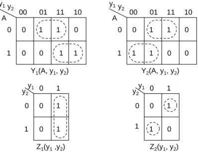
signal A. . . . 21 Figure 2.6 Karnaugh maps derived from the excitation table of the 2-bit counter. 23 Figure 2.7 Circuit of the asynchronous 2-bit counter. . . 23 Figure 3.1 Overview of the structure of the proposed asynchronous DC-DC
con-verter. . . 29 Figure 3.2 Simplified architecture of the SC DC-DC converters network. . . 30 Figure 3.3 Arrangement of switches and capacitors in the SC converter. . . 30 Figure 3.4 Possible topologies that can be realized with the arrangement of
ca-pacitors and switches shown in Fig. 3.3. M represents the conversion ratio achieved when switching between two of the shown arrangements. 31 Figure 3.5 Timing diagram when the converter operates under: (a) regular load,
(b) load that exceeds the limits. . . 32 Figure 3.6 The state-flow diagram of the asynchronous controller. . . 33 Figure 3.7 The Mode Detector circuit showing all blocks and signals used in the
Figure 3.8 Photomicrograph of the proposed converter. The main building blocks are numbered as follows: (1) Capacitors, (2) Switches, (3) Signal router, (4) Mode detector, (5) Comparator, (6) Asynchronous controller and (7) Mode Selector . . . 37 Figure 3.9 Measurement of the output voltage and the drive signal S1 of the
con-verter while loaded with 10kΩ and 100pF : (a) shows the output voltage start up response from 0V to 0.95V with a settling time of 408ns, (b) presents the regulation at Vout = 1.07V with a peak to peak output
rip-ple of 53mV while the asynchronous drive signal frequency is 3M Hz, (c) presents the regulation at Vout = 0.66V with a peak to peak
out-put ripple of 36mV while the asynchronous drive signal frequency is 3.6M Hz , (d) presents the regulation at Vout = 0.36V with a peak
to peak output ripple of 32mV while the asynchronous drive signal frequency is 1.9M Hz. . . . 38 Figure 3.10 The graphs show results of the efficiency measurements versus the load
current at different output voltages. The three types of efficiency de-fined in section 3.3 are shown in each subfigure:(a) presents the effi-ciencies at Vout = 1V , (b) presents the efficiencies at Vout = 0.95V , (c)
presents the efficiencies at Vout = 0.65V , (d) presents the efficiencies at
Vout = 0.6V , (e) presents the efficiencies at Vout = 0.35V , (f) presents
the efficiencies at Vout = 0.3V . . . . 39
Figure 3.11 Measurement of (a) line regulation at an output voltage of 0.53V with an input step from 1V to 1.2V resulting in a 16 mV change in the output voltage, (b) load regulation at an output voltage of 0.63V with a load step from 68µA to 1µA resulting in an 42 mV change in the output voltage. In both measurements, the variations in the drive signal’s frequency is apparent. . . 40 Figure 3.12 The graph shows the measurement results of the operating frequency
at different output load values. These measurements are done at Vout of
0.3V , 0.6V and 0.95V with conversion ratios of 1 3,
2
3 and 1, respectively.
The points at which additional switches are turned on are shown on the graph. . . 41 Figure 4.1 Asynchronous Controller Karnaugh maps extracted form the excitation
table for: (a) the outputs (S0, S1 and S2), (b) next states (Y0, Y1 and
Figure 4.2 The full digital circuit of the Asynchronous Controller block that ap-pears in Fig 3.1. . . 48 Figure 4.3 The enabling circuit within the Signal Router. When Support signal
is low GX add = GN D. When Support signal is high GX add = GX. . 50
Figure 4.4 The Mode Selector circuit consisting of multiplexers and non-overlapping signal generators. . . 50 Figure 4.5 The dual threshold comparator based on OTA and 3 current mirrors.
VA∗ and VB∗ are the unbuffered outputs of the comparator. . . 51 Figure 4.6 The results of the DC analysis of the comparator: (a) Show the
input-outputs voltage characteristic, (b) Shows the comparator drain currents Vs input voltage characteristics. . . 52 Figure 4.7 The transition from Asynchronous to Synchronous Drive Mode when
the load exceeds the limit. . . 53 Figure 4.8 Efficiency simulation results versus the load current at (a) Vout = 1V ,
(b) Vout = 0.6V , (c) Vout= 0.35V . The three types of efficiency defined
in section 3.3 are shown. . . 54 Figure 4.9 Efficiency PLS versus the load current at (a) Vout = 1V , (b) Vout =
0.6V , (c) Vout = 0.35V . The three types of efficiency defined in section
3.3 are shown. . . 54 Figure 4.10 Additional efficiency experimental results versus the load current at (a
)Vout = 1.1V , (b) Vout = 0.7V , (c) Vout = 0.38V . The three types of
efficiency defined in section 3.3 are shown. . . 55 Figure 4.11 Additional measurements of the output voltage of the converter while
loaded with 10kΩ and 100pF : (a) Vout going from 0V to 0.35V in
1.36µs, (b) Vout going from 0V to 0.64V in 468ns. . . . 56
Figure 4.12 Output voltage when the load current exceeds the limits while the Mode Detector is deactivated: (a) when the converter is using a conversion ratio of M = 1/3 the ripple is 304mV , (b) when the converter is using a conversion ratio of M = 2/3 the ripple is 200V , (c) when the converter is using a conversion ratio of M = 1 the ripple is 196mV . . . 56 Figure 4.13 Measurement of the output voltage ripple (∆Vout) versus the loading
current at different conversion ratios (M ): (a) M = 1, (b) M = 2/3, (c) M = 1/3. . . . 57 Figure A.1 Charging a capacitor from a DC supply (e.g. battery) . . . 71
List of Appendices
List of Abbreviations and Symbols
Abbreviations:
ADM Asynchronous Drive Mode.
AFS Automatic Frequency Scaling.
AGPC Adaptive Gain-Pulse Control.
ASM Asynchronous State Machine.
CMOS Complementary Metal-Oxide-Semiconductor.
DC Direct Current.
DFS Dynamic Frequency Scaling.
DPWM Digital Pulse Width Modulation.
DVS Dynamic Voltage Scaling.
EMI Electromagnetic Interference.
MIM Metal-Insulator-Metal.
MOS Metal-Oxide-Semiconductor.
NMOS N-type Metal-Oxide-Semiconductor.
PFM Pulse Frequency Modulation.
PLS Post-Layout-Simulation.
PMOS P-type Metal-Oxide-Semiconductor.
PWM Pulse Width Modulation.
SC Switched Capacitor.
SDM Synchronous Drive Mode.
Symbols:
∆Vout Output voltage ripple.
η Efficiency.
ηlin Linear efficiency. Max. possible efficiency for a SC DC-DC converter.
ηpar Efficiency of a SC DC-DC converter including only losses in conduction
and parasitics (i.e. total efficiency without switching and control losses). ηconv Total efficiency of SC DC-DC converter without losses in control circuit.
ηtotal Total efficiency of SC DC-DC converter including losses in control circuit.
C Capacitance.
E Energy.
Ectrl Energy consumed (lost) in control circuit.
Ein Input energy.
Eout Output energy.
Epar Energy lost in parasitics.
Esw Energy lost in switching (operating the switches in the SC converter).
f Frequency.
L Length of the channel of a MOS transistor. M Conversion ration of a SC DC-DC converter.
P Power.
Pin Input power.
Pout Output power.
Pdynamic Dynamic power consumption.
Pstatic Static power consumption.
R Resistance.
VDD Supply voltage.
Vin Input voltage.
VN L Output voltage at no load.
Vout Output voltage.
Chapter 1
Introduction
1.1
Motivation
Modern technologies have enabled engineers to integrate devices with various function-alities into silicon chips that are very compact. Nowadays these devices are part of our daily life. Among the key contributers to our luxurious life style are portable devices. They have affected our life style in many ways. With recent incorporation of portable devices in medicine, the way we think about treatment of patients has expanded. Biomedical implants have offered solutions to numerous medical problems [15].
In biomedical implants, the size of the device and the battery life-time are of great impor-tance. Since a lot of the implants tackle chronicle or permanent health issues, the implants should be as convenient as possible for the patients to live with. That is to say, smaller and lighter implantable devices are more convenient for patients. The size of implants is reduced by integrating what can be integrated of the circuitry into a single chip. While, the prolonga-tion of the battery life is done by minimizing the power consumpprolonga-tion of the implant’s circuits as much as possible [13, 14, 33, 34] and finding other alternative power sources [9, 12, 28, 39]. Most electronic devices nowadays are designed using the CMOS technology. The power consumption of CMOS circuits is given by [36]:
P = Pstatic+ Pdynamic = V2 DD R + f CV 2 DD (1.1)
where VDD is the power supply voltage, R is the equivalent resistance of the circuit between
the power supply and ground, f is the operating frequency and C is the capacitance between the output of the circuit and ground. A very interesting fact can be seen in Eq. (1.1). The power consumption of CMOS circuits is proportional to the square of the power supply voltage. Hence, if we reduce VDD by a certain amount, we reduce the power consumption of
the circuit quadratically. What Eq. (1.1) does not tell us is that, reducing VDD might affect
between speed and VDD. Reducing VDD slows down the circuit. The other fact that can be
seen in Eq. (1.1) is that, the frequency of operation is directly proportional to the dynamic power consumption. This implies that, reducing the frequency of operation of a system also reduces its power consumption. On the other hand, lower operating frequencies leads to slower systems.
Dynamic Voltage Scaling (DVS) and Dynamic Frequency Scaling (DFS) are two techniques that exploits the previously mentioned facts [25, 31, 47]. By adaptively adjusting the power supply voltage to the conditions of operation of a system, we can minimize power consump-tion. This is the basis of the DVS technique. Likewise in DFS, by adaptively adjusting the operating frequency of a system, or operating completely asynchronously [24], according to the workload of the system, the power consumption is minimized. These two techniques can be very helpful with extending the battery life-time in biomedical implants.
To implement the DVS technique under battery powered devices, DC-DC converters are used [10, 19, 22, 30, 40]. These converters are able to reproduce levels of DC voltages different than the input voltage (battery voltage is this case). There are various types of DC-DC converters that can be used to address the needs of the DVS technique, but since we are also considering the size of the device, we have to try to propose and demonstrate a DC-DC converter that is suitable for integration on-chip.
There are three main families of DC-DC converters: Resonant converters, Switched Capac-itor (SC) converters and linear regulators [7]. The resonant DC-DC converter uses inductors and capacitors to achieve conversion. They are proven to be top notch when it comes to the conversion efficiency. However, on-chip inductors are huge, have a low quality factor, and can cause electromagnetic interference (EMI) problems [20, 44, 46]. On the other hand, linear regulators are very easy to design and integrate, But their conversion efficiency is con-siderably lower than the Resonant converters, especially when the output voltage is much lower than the input voltage [6, 17]. The last family of DC converters is the SC DC-DC converters. It was shown in literature that this family of converters can be implemented completely on-chip while providing good conversion efficiency levels [11, 26, 29, 40, 43]. From this discussion we conclude that the most suitable family of DC-DC converters that adheres to our initial requirements is the SC DC-DC converters.
1.2
Objectives and Challenges
The DC-DC converter that we are designing here should handle battery powered devices, such as implants, that use DVS and/or DFS. Keeping that in mind, we will consider the following goals:
– In order to reduce the size and weight of portable device (implants), The DC-DC converter should be completely integrated on chip.
– Devices that operate with DVS requires from the DC-DC converter the ability to pro-vide different levels of voltages from a single voltage source (in this case the battery). In addition, the change between the different levels of output voltage should be achieved as quick as possible.
– To extend the battery life-time of the powered device, the DC-DC converter should consume the lowest power possible. That implies that, the conversion efficiency under various operating conditions must be high.
– As we will explain in the coming chapters, to maximize the efficiency of a SC DC-DC converter, the operating frequency of the converter should be adapted to the loading conditions. A frequency control module should be implemented to take care of this task.
– To provide the best conversion efficiency at different levels of output voltage, the SC DC-DC converter has to adjust its switching topology. This fact will be elaborated in later chapters.
– Finally, since the circuits in battery powered implants are of low power nature, the designed DC-DC converter must maximize the efficiency around such values of power. The list of goals that we just established faces various challenges. To fully integrate a SC DC-DC converter we will need to use on-chip capacitors. The capacitance that the on-chip capacitors provide is not as high as the capacitance of external capacitors. This has two consequences on the performance of a SC DC-DC converter; the reduction of the maximum output power that can be supplied by the SC DC-DC converter and the increase in the output ripple. The latter can be reduced by using higher switching frequencies but that solution has side-effects on other performance measurements concerning efficiency and dynamic power loss. This reduction in the maximum output power is not a main concern since we are targeting low power applications.
Improving the response time of a SC DC-DC converter is yet another challenge. In SC DC-DC converters, the response time depends on the sizes of the capacitors and switches used as well as the frequency of operation and the output power. This means that, the
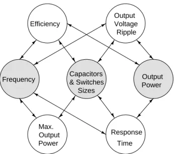
Efficiency Frequency Output Voltage Ripple Max. Output Power Response Time Sizes Capacitors
& Switches OutputPower
Figure 1.1 The SC DC-DC converter performance measurements and their dependence on the operating frequency, output power (output voltage and loading current) and sizes of the components
response time is also tied to a bundle of other performance measurements. In fact, all the other major performance measurements are dependent on the following parameters: the frequency of operation, output power (output voltage and loading current) and the sizes of the capacitors and switches. Note here that by ”size of switches” we are referring to the width (W) and length (L) of the CMOS switches, which determines the ON resistance and the gate capacitance of the CMOS transistor.
Figure 1.1 illustrates which performance measurements depend on which parameters. This complex relationship between the performance measurements makes the design process of the SC DC-DC converter challenging. The frequency of operation and the size of components are design parameters, while the output power is a parameter that is determined solely by the load demand for power. Therefore, when trying to find an optimum, the designer have about three or more levels of sweeps. One sweep is done on the size of capacitors, and another one or two sweeps are done for determining the size of switches (NMOS, PMOS). Finally the frequency of operation is swept in a certain range to optimize the performance measurements. Furthermore, if for any reason some elements of the design changed, the optimization process might have to be redone.
The last challenge that faces this design is implementing an adaptive frequency control method. The control should consume the least amount of power while maintaining a good
level of conversion efficiency for the SC DC-DC converter. In addition, a promising strategy is to ensure that the control adapts automatically the frequency of operation to the operating conditions of the SC DC-DC converter.
1.3
Contributions
In light of the goals that we have set and the challenges that have been mentioned, the contributions of this thesis are as follows:
– We have designed and implemented a new fully integrated asynchronous SC DC-DC converter structure that is capable of supporting ultra-low-power systems, such as biomedical implant circuitry, with an adjustable output voltage. This converter takes advantage of variable conversion ratio and scalable operating frequency to enhance the conversion efficiency under different operating conditions. To ensure robustness of the design, the SC DC-DC converter is equipped with a synchronous back-up mode that is triggered when the loading power exceeds the maximum load current.
– Moreover, in chapter 3 and 4 we developed an asynchronous controller capable of not only automatically scaling the operating frequency but also scaling the size of the switches used depending on the loading conditions. Both of these techniques help reducing the power losses in the charge transfer switches in the converter, as well as the dynamic power losses in the controller.
– We have also constructed a smart limit detection scheme in the control to allow a Mode Detector block to identify when the loading power exceeds the maximum output power. As we will explain in the coming chapters, to control the switches’ sizes, we made use of the same smart detection scheme to allow the Mode Detector to turn ON additional parallel switches when needed. We also designed the Mode Detector so that it can be very easily expanded to support as many levels of additional parallel switches as desired. This is done by simply repeating (cascading) a basic block in the Mode Detector’s circuitry.
1.4
Thesis Organization
This master’s thesis is organized as follows. First, an introduction to fundamentals of conversion mechanism and efficiency in SC DC-DC converters as well as a literature review is presented in chapter 2. Chapter 3 discusses the design of a low-power asynchronous step-down DC-DC converter for implantable devices. Chapter 4 provides additional details and results for the proposed SC DC-DC converter. A general discussion about the complete
thesis is provided in chapter 5. Finally, the thesis is concluded and future improvements are suggested in chapter 6
Chapter 2
Basic Switched-Capacitor Converters
Principals And Literature Review
2.1
SC DC-DC Converters Fundamentals
A brief look on the fundamental operation of a SC DC-DC converter will help the reader to better understand the topic discussed in this thesis. Terms such as: conversion ratio, conversion efficiency and drive signals are explained in this section. Moreover, some of the recent work on step-down SC DC-DC converters are reviewed. But before proceeding, two simple questions should be answered. What is a SC DC-DC converter? And how does it convert one voltage value to another?
2.1.1
Conversion Mechanism and the Conversion Ratio
A switched-capacitor (SC) DC-DC converter (may also be known as a charge pump) is a block that takes an input voltage (Vin) and outputs a different value of a voltage (Vout).
This block consists of a network of capacitors and switches, and operates in two phases or more. If the output is higher in voltage than the input, the conversion is called a ”step-up” conversion. Vice versa, if the output voltage was lower than the input, the conversion is called a ”step-down” conversion. The type of conversion that we will be focusing on in this thesis is the step-down conversion.
Most of the SC DC-DC converters operate in two phases: a charging phase and a discharg-ing phase. The chargdischarg-ing phase takes place when a group of capacitors in the network are connected to the DC power source (input) to get charged, while the discharging phase starts when this group of capacitors are connected to the load (output) to discharge. Since these capacitors are responsible of transferring the charge from the input to the output, they are sometimes known as the charge-transfer capacitors [29, 45]. Likewise, some authors refers to them as the pumping capacitors because they ”pump” the charge from the input to the output[11, 40].
+ − Vout Load Vin C C C C Vout Load + − Vin C C Vin/2 + _ Vin/2 + _ Vin/2 + _ Φ1 Φ1
(a)
(b)
(c)
Charging Phase Φ1 Discharging Phase Φ1
Φ1 Φ1 Φ1
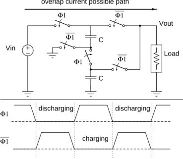
Figure 2.1 An example of the operation of a SC series-parallel configuration in stepping down an input voltage, (a) shows the complete network of capacitors and switches. Φ1 and
Φ1 are the control signals for the switches (b) shows the equivalent circuit when the switches
controlled by Φ1 are ON, (b) shows the equivalent circuit when the switches controlled by
Φ1 are ON.
There maybe several different configurations of connecting the capacitors in each of these phases, and each configuration has its own characteristics. In this project, we adopted the ”Series-Parallel” configuration. Not only is this configuration simple, but also it offers a better performance at lower switching frequencies [37]. The reason for pursuing lower switching frequencies will be explained soon.
An example of a series-parallel step-down SC DC-DC converter is presented in Fig. 2.1. Two capacitors and five switches are connected in a network, and the switches are controlled by two signals Φ1 and Φ1 (Fig. 2.1(a)). In the first phase (charging phase), Φ1 turns ON
a set of switches which will connect the two capacitors in series (Fig. 2.1(b)). Since both capacitors have the same value of capacitance C, each will be charged to Vin/2. Assuming of
course that enough time was provided for the capacitors to be fully charged. In the second phase, the switches connected to Φ1 turn OFF, while the ones connected to Φ1 turn ON. This
will connect both capacitors in parallel with the output load resulting in an output voltage Vout = Vin/2. As current starts to flow in the load, the charge stored in the capacitors will
deplete and the output voltage will drop.
In the previous example, Vin was converted to Vin/2. If the load was not connected, the
output voltage would have remained at half the input. The ratio of the output voltage to the input voltage, when no load is connected, is called the conversion ratio (M ).
M = VN L Vin
(2.1) Notice that, the output voltage (Vout) of a SC DC-DC converter with conversion ratio (M )
cannot exceed the output voltage at no load (VN L). For the last example, the conversion
ratio M = 1/2 and Vout can have a maximum value of VN L = Vin/2. Now that we explained
how the conversion is carried out in a series-parallel SC DC-DC converter, let us see what effects the efficiency in the conversion process.
2.1.2
Efficiency of SC DC-DC converters
In general, the conversion efficiency of any DC-DC converter can be defined as the per-centage of energy delivered to the load (Eout) with respect to the energy taken from the
supply (Ein) [30]: η = Eout Ein × 100% (2.2) where, Eout= ∫ T Poutdt (2.3) Ein= ∫ T Pindt (2.4)
From this definition, if we try to derive the efficiency of the circuit in Fig. 2.1, we will find that: ηlin = 1 M Vout Vin × 100% (2.5)
An interesting fact can be seen in Eq. (2.5). The conversion efficiency does not depend on the size of the capacitors nor on the resistance in the charging path. Rather, the efficiency of a SC DC-DC converter only depends on Vout, Vin and the conversion ratio M . This equation
that a SC DC-DC converter can achieve [21, 29]. The name ”linear efficiency” is given to this term because the efficiency drops linearly as Vout decreases. A detailed derivation of Eq.
(2.5) is provided in Appendix A. To maximize the efficiency under different output voltages, the conversion ratio M should be adjusted accordingly. Moreover, by substituting Eq. (2.1) in Eq. (2.5), the linear efficiency would be written as:
ηlin =
Vout
VN L
× 100% (2.6)
This equation implies that the efficiency of a SC DC-DC converter is maximum when Vout =
VN L. Note that Eq. (2.5) represents the efficiency of transferring the charge (conduction)
between the input and output in a SC DC-DC converter. In Eq. (2.2), If Ein was redefined
as the sum of the energy delivered to the load (Eout) and the energy wasted in the conversion
process (Eloss), the efficiency in Eq. (2.2) can be rewritten as:
η = Eout
Eout+ Eloss × 100%
(2.7) Eloss is a combination of various kinds of loss mechanisms in a SC DC-DC converter. To
enhance the efficiency of the converter, we should define these losses. in [30], Ramadass et Chandrakasan identified four different types of losses.
Conduction losses (Econd): The first type of losses, Econd, is due to the power dissipated
in internal voltage drops in the SC network. This term is the intrinsic loss that occurs when a capacitor charges from a battery (refer to Appendix A). It is the same loss that led to the definition of the linear efficiency in Eq. (2.5). It depends mainly on value of Vout, Vin and
the conversion ratio M . As discussed earlier, this loss is reduced by keeping Vout close to VN L
and using a SC DC-DC converter with variable conversion ratio.
Parasitic losses(Epar): The second term Epar, is the energy loss due to stray parasitic
capacitances in the circuitry. Some parasitic capacitances for example, would store certain amount of energy from the source during the charging phase then discharge to ground during the discharge phase. The nature of this loss makes it very hard to control. It can depend on the technology, type of capacitors used and the configuration of the SC netwrok. In addition, we can include current leakages in ESD protections circuitry (if any).
Switching losses(Esw): The third loss term Esw, is the energy used to operate the switches
in the network. Since the switches used normally in a SC DC-DC converter are MOS switches, a certain amount voltage should be applied to the gates to turn them ON in one phase, and
then the gates are discharged to ground in the next phase. This is very similar to way the stray parasitic capacitance losses happen. One method to reduce these losses is by using smaller switches. This however increases the ON resistance of the switches, which can affect other performance measurements such as the maximum output voltage or current. A more reasonable approach is to vary the switches’ size according to the load current. Another method of reducing this term is by reducing the switching frequency. Of course, since the frequency also affects other performance measurements, it suggests that potential benefits could be derived from a design based on a variable frequency approach.
Control losses (Ectrl): Finally, Ectrl is the energy lost in the control circuitry. This term
is the main reason why most new converters operate with digital control circuitry, which can be designed to have negligible static power consumption. The dynamic power consumption however is still an issue. Because all the current digital control circuits depend on a constant frequency clock, a certain amount of constant dynamic power loss exists. Traditionally, SC DC-DC converters were designed as open-loop converters where a control circuit was not needed. These kinds of losses may not be present in open-loop designs.
By combining all the losses that were mentioned above, the total conversion efficiency of the SC DC-DC converter becomes:
ηtotal =
Eout
Eout+ Econd+ Epar+ Esw + Ectrl
× 100% (2.8)
Note that in Eq. (2.8), if Eout decreases while the energy losses are constant, the
effi-ciency decreases rapidly. To maintain the effieffi-ciency high, the losses should also decrease as Eout decreases. In other words, the energy losses should scale with the output current (load).
In this work we will design various techniques, such as complete asynchronous control and automatic switch size scaling, to make sure the energy losses scale with the output load. Un-fortunately, the energy losses cannot be reduced indefinitely because there are some leakages and static power losses in CMOS circuits that are not avoidable.
Finally, we should mention here that the efficiency can be similarly defined using the average power instead of the energy. Both definitions will lead to the same result, but to be consistent with the analysis of the losses found in literature and the derivation of the linear efficiency presented in appendix A, the definition of the energy efficiency will be used throughtout this thesis.
Vout Load + − Vin C C Φ1 Φ1 Φ1 Φ1 Φ1 Φ1 Φ1 discharging charging discharging overlap current possible path
Figure 2.2 An example of a non-overlapping drive signals that should be used to avoid overlapping drive signal currents.
2.1.3
Drive Signal Requirements
A drive signal is the signal that controls the MOS switches in the SC DC-DC converter. Alternating between 0V and Vdd, these signals turn ON and OFF the switches to change the
connection of the capacitors in the charging and discharging phases. Typically, SC DC-DC converters operate with a drive signal and its complement. The most important requirement of these signals is to be non-overlapping. Fig. 2.2 shows an example of a SC DC-DC converter and the patten of a drive signal (Φ1) and its complement (Φ1) that should be used to drive
it. If the drive signals overlap, currents may flow through undesired paths. The example in Fig. 2.2 shows one of the possible undesired paths of current that could happen if Φ1 and
Φ1 overlap. This path creates a connection between Vin and Vout leading to a current flowing
directly form the input to the output, which reduces the conversion efficiency significantly and affects the output voltage regulation.
2.2
SC DC-DC Converters Control Methods
There are various control methods that exist in the literature for SC DC-DC converters. The main purpose of a control method is to regulate the output voltage at a desired level under different loading conditions. In this section, we will take a brief look at the main control methods for SC DC-DC converters, which are pulse width modulation (PWM) control and
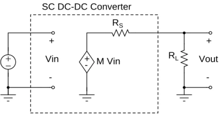
+ − Vin SC DC-DC Converter M Vin RS RL + -+ - Vout +
-Figure 2.3 A simplified model of a SC DC-DC converter consisting of a dependent voltage source and a series resistance.
pulse frequency modulation (PFM) control. Before we go into these closed loop control methods, we will look at how an open loop SC DC-DC regulates the output voltage.
2.2.1
Open Loop Control
When operating a SC DC-DC converter in an open loop, the output voltage will depend on the operating frequency (f ) and the load value. To elaborate, we construct a simple model of a SC DC-DC converter consisting of a dependent voltage source with a value of M Vin in series with a resistance RS (Fig. 2.3). M in this model is the conversion ratio of
the converter. In Fig. 2.3, the SC DC-DC converter is loaded with a load resistance RL.
Since RS and RL are connected in series, they form a voltage divider. Thus, the output
voltage Vout depends on the values of RS and RL. For Vout to be equal to M Vin, RL should
have a very high impedance (No load) or RS has to equal zero Ohms. We will see in the
coming discussion that the latter is impossible. As RL decreases (the load increases) or as
RS increases, Vout start to decrease below M Vin.
The operating frequency (f ) indirectly impacts Vout by affecting RS. In 2008, Seeman and
Sanders presented a detailed analysis of SC DC-DC converters [37]. One of the conclusions of their work was the fact that in a SC DC-DC converter, RS decreases as the operating
frequency (f ) increases. Once the operating frequency reaches a certain value (fc), RS
becomes constant (independent of f ). The value of fc depends on the sizes of the capacitors
and switches used, as well as the topology of the SC DC-DC converter. At that frequency the series resistance of the SC DC-DC converter is minimum (RS = RSC,min). Note that for
f < fc, the output voltage (Vout) is proportional to the operating frequency. This fact can
be exploited to design closed loop control methods for regulating the output voltage in SC DC-DC converters.
2.2.2
Pulse Width Modulation (PWM) Control
One of the main control methods for regulation the output voltage in SC DC-DC convert-ers is the Pulse Width Modulation (PWM) Control. Rather than varying the drive signal frequency to adjust the output voltage, the PWM uses a constant frequency drive signal with a variable duty-cycle. The fundamental idea of PWM is to adjust the ratio between the charging and discharging cycles, and thereby the amount of charge transfered from input to output is controlled and the output voltage is regulated at a desired level.
Unlike inductor based converters, the change in the output voltage that can be obtained from only controlling the duty-cycle in a SC DC-DC converter is limited. Hence, when the load becomes high, it is necessary to increase the operating frequency to maintain the output voltage at a constant level. This is the main disadvantage of using PWM control for this type of converters. Furthermore, this control method requires more complicated circuits and techniques than the PFM control method.
2.2.3
Pulse Frequency Modulation (PFM) Control
The Pulse Frequency Modulation (PFM) control method is a simple and effective way to regulate the output voltage in SC DC-DC converters. The main idea of this control method is to activate a driving signal (clock signal) when the output voltage is lower than the desired level (a reference voltage) and then deactivate it when the voltage is higher.
A basic PFM control is constructed with three basic circuits: a clock generator, a logic gate and a hysteresis comparator. The comparison between the output voltage and the reference voltage is done by the hysteresis comparator. With the help of the logic gate, the output signal from the comparator works as a mask for the clock signal allowing it to pass to the converter when the output voltage is lower than the reference, and stopping it when the output voltage is higher than the reference. Because this method of control requires a hysteresis comparator to operate, some authors call it hysteresis control [38].
One advantage of the PFM is that it can reduce the switching losses of the converter at light loads. However, the clock is constantly running, which leads to a constant dynamic power loss in the control circuit. Also, the frequency of the clock used is the maximum frequency that the PFM control can achieve. Hence, this frequency should be carefully chosen according the maximum load of the converter.