HAL Id: tel-00998677
https://tel.archives-ouvertes.fr/tel-00998677
Submitted on 2 Jun 2014HAL is a multi-disciplinary open access archive for the deposit and dissemination of sci-entific research documents, whether they are pub-lished or not. The documents may come from teaching and research institutions in France or abroad, or from public or private research centers.
L’archive ouverte pluridisciplinaire HAL, est destinée au dépôt et à la diffusion de documents scientifiques de niveau recherche, publiés ou non, émanant des établissements d’enseignement et de recherche français ou étrangers, des laboratoires publics ou privés.
Indirect Analog / RF IC Testing : Confidence &
Robusteness improvments
Haithem Ayari
To cite this version:
Haithem Ayari. Indirect Analog / RF IC Testing : Confidence & Robusteness improvments. Other [cond-mat.other]. Université Montpellier II - Sciences et Techniques du Languedoc, 2013. English. �NNT : 2013MON20062�. �tel-00998677�
!
!
"
#"
$
%
"
! " # $ ! % # $&% '()%** + ,- # $ ! % # $&% '()%** $ ' * # % # $&% '.)*, % ) /0 # 1 # 2 ( ')&( % * % # % # $&% ' ()%** 3 $ 4 # ) ! # &5 3 6 7 - # $ ! % # $&% ' ()%** ) * $ # * 8 $ 1 # 2 * ))' ()%** )&
'
!( )
*
!
" #$ $ % &# ! #$ ! ' ! ( ) * $ + #$ , ! ! , % &# ( - *
Test Indirect des circuits Analogique et RF: Contribution
pour une meilleure précision et robustesse
!" # ! " #$ % ! &' ( ) * + * , # * -. / 0 1 -. 2 3 4 $ 5 * 2 6 ( 5 ) 7 *
Indirect Analog/RF IC testing: Accuracy & Robustness
improvements
©Copyright by Haithem Ayari 2013 All right reserved
*
*
* ) * ( + ' ,"& $ ( -. / , % ! ( + ( 0 + * ( 1 * ) 23 4 + ! + ( + ! ! + ( * ( ' & + + + ( 5 * ( ' , * ( 6 37 + ( ' , 8 "#$ + + ( ) ( ! + + + + (
* , * ( &) ( 5 8 * * * (+ + ( 2 , (( * 8 + (( ( ( 8 4 2 " 5 ( ), ( +2 # ( ( *9 5 (( 2 /2 # 5 ( . * $ 2 5 * * 5 ( * ( 2 # 5 + 8 5 8 * + 5 * + .2 # &) 8 ( * 2 5 ( ( 8 ( * . + (( (( ( 2 * 5 + ( * " 5 8 2 9 5 ( * (+ * ( + ( 4 2 , 8 ( * ( ( ( 85 8 4 + ( 2 5 ( * 8 ( * 5 ( + * * + + ( 82 , + ( + 4 : $;2 . 5 * 2 +5 *9 * ( * 2 , + 4 8 + 8 " 2 , + ( 2 5 + ( ( 2 & 8 4 ( 8 2 " 5 8 * . ( *, ( &) 8 * + ( *, 2 ( 8 * : %"2 $2 ; + 8 ( *9 ( 8 $ ( : 2 2 ;2 5 8 * * ( + * ( * (( ( $ 2 , . + (+5 5 * 8 < * * ( 8 ( + +2
. . * 5 ( = = 2 5 ! ! 2 * 5 ( . ( 2 5 5 = (( > = (( . * 2 , ' 5 . 0 ( ( 2 ( ( ( 5 * (( . * = 2 - 5 * = . ? @ .2 - 5 * ! 5 = (( ( 2 - 5 > ( = .5 * ! . 2 ) ( * 0 * ( * :8 ( ;2 - (( 5 A * ( * . ? (( * ' ( 2 -5 ' * " 5 2 - 5 * 0 * ( ! 6 2 ! = = = = ( ! ( 0 * B ( ! @ ( 2 #( @ 5 * * 5 ( . * ? ! B ( . 2 ! + + ! 6 : ;2 . 5 0 * 2 " 5 0 * ( 2 ' > ' ' ! "2 ? ( 2 # 5 5 5 (( ( ! ' 2 5 ! ( = 2 ( * ( * ( * 2 * * 0 ( * 2
.
!"
I.1 Introduction ... 5
I.2 Industrial test generalities ... 7
I.3 Analog/RF ICs testing specificity ... 9
I.3.1 Faults in analog/RF ICs ... 9
I.3.2 Analog/RF ICs test: current practice ... 9
I.4 Cost-reduced RF IC testing strategies ... 11
I.4.1 Integrated test solution ... 11
I.4.2 Loopback testing ... 12
I.4.3 Indirect testing... 12
I.5 Conclusion ... 16
#
$
%
#
II.1 Introduction ... 18II.2 Classical implementation of prediction-oriented indirect test... 19
II.3 DC-based indirect test strategy ... 20
II.4 Presentation of the test vehicles ... 21
.
II.4.2 Power Amplifier ... 22
II.4.3 RF Parameters ... 22
II.4.3.1. Gain ... 22
II.4.3.2. Noise Figure (NF) ... 23
II.4.3.3. Gain Compression ... 24
II.4.3.4. Third Order Intercept Point ... 25
II.5 Benchmarking of some machine-learning regression algorithms ... 27
II.5.1 Multiple Linear Regression ... 27
II.5.2 Multivariate Adaptive Regression Splines ... 28
II.5.3 Artificial Neural Network ... 29
II.5.4 Regression Trees ... 29
II.5.5 Test case definition ... 30
II.5.6 Results and discussion ... 32
II.6 Limitations & bottleneck of the conventional indirect test scheme ... 36
II.6.1 Prediction confidence: flawed predictions ... 36
II.6.2 Dependency of model performances with respect to TSS ... 39
II.7 Conclusion ... 43
&'
(
&'
III.1 Introduction ... 46III.2 Benchmark of some feature selection techniques ... 47
III.2.1 Variable subset selection techniques ... 47
III.2.1.1. Filters ... 47
III.2.1.2. Wrappers... 49
III.2.2 Test case definition ... 51
III.2.3 Results and discussion ... 52
III.3 Proposed IM selection strategy ... 54
III.3.1 Dimensionality reduction of IM-space ... 55
III.3.2 Search space construction ... 56
III.3.3 Optimized IM subset selection ... 56
III.3.4 Results and discussion ... 57
.
)
'
$
*
'
IV.1 Introduction ... 61
IV.2 Outlier definitions ... 62
IV.2.1 Process-based outlier... 62
IV.2.2 Model-based outlier ... 62
IV.3 Redundancy-based filter for model-based outliers ... 62
IV.3.1 Principle ... 62
IV.3.2 Experimental results using accurate predictive models ... 64
IV.4 Making predictive indirect test strategy independent of training set size ... 69
IV.5 Model redundancy to balance the lack of correlation between IMs and RF performance parameters ... 74
IV.6 Different implementation schemes of redundancy ... 77
IV.6.1 Motivation ... 77
IV.6.2 Principle of augmented redundancy CPC schemes ... 78
IV.6.3 Experimental Results ... 81
IV.7 Conclusion ... 85
#+
!
,
,
,'
,#
,,
C
The recent advances in fabrication and packaging technologies have enabled the development of high performance complex Radio Frequency (RF) chips for a wide range of applications. RF chips, which are the focus of this work, are on the leading edge of technological developments and rise a significant number of production problems. Considering first the global production costs of high volume production of Integrated Circuits (ICs), these costs include design, manufacturing and test costs. In the recent years it has been observed that i) design costs have grown significantly but not drastically due to improved design productivity, ii) manufacturing costs have remained reasonably flat because of technological advances, iii) test costs have dramatically increased because of ever demanding requirements on the test instrumentation. Note that this is true for today highly integrated digital System-on-Chip (SoC) and System-in-Package (SiP) products manufactured in nanometer technology for which an Automatic Test Equipment (ATE) equipped with high-speed digital resources are required. But it is even emphasized for analog and RF products for which not only high-speed but also high-precision analog and RF test resources are required.
Indeed the conventional approach for testing analog and Radio Frequency (RF) devices is specification-oriented testing, which consists in measuring the majority or totality of the circuit performance parameters defined in its datasheet and comparing these values to pre-defined tolerance limits in order to sort the fabricated circuits as good or bad circuits. Typical
RF measurements include “Gain”, “Noise Figure” (NF), “Third-Order Intermodulation” (IP3), just to name a few... This strategy, summarized by Fig. 1, aims at adapting the test to each kind of circuit, according to its function and performances. Another strategy, called structural-oriented testing, has been developed over the years. This strategy relies on a list of fault models to be applied to any kind of circuit regardless of its function. The specification-oriented strategy was and continues to be predominantly adopted due to the lack of widely applicable fault models. The clear advantage of specification-oriented testing is that it obviously offers good test quality, but at extremely high cost due to the required sophisticated test equipment and long test time. In addition, testing is usually applied at two different levels of the manufacturing process, i.e. first at wafer-level after silicon wafers have been fabricated
7
and then at package-level once circuits have been encapsulated. For all these reasons, testing costs for RF products are becoming the largest part of the overall costs [1] [2].
Fig. 1: Specification-based test strategy
Beyond the cost problems, technical measurement capabilities are also a challenge, especially at wafer level which is of crucial importance to guarantee Known-Good-Dies (KGD) [3]. Indeed RF measurements are severely impacted by the environment: parasitic elements, improperly calibrated equipment, external radiations, etc. Assuming a complex RF chip with limited access, it is very difficult if not impossible to get the correct RF parameters measurement even by using expensive ATE equipped with high-performance resources. Consequently due to the high cost and technical problems, specification-based RF IC testing is the major bottleneck to reduce the overall manufacturing cost in semiconductors industry.
In this context, industrials are continuously looking for novel low-cost test strategies for analog and RF devices to overcome the cost issue. Several techniques such as analog Built-In-Self-Test (BIST) and Design for Test (DfT), which are no longer based on RF specification measurements, have been investigated. They are based on signature measurements to classify good and bad devices. Another promising solution to lessen the burden of specification testing is indirect testing, also called in literature alternate testing. In this strategy, the results of specification testing are derived from a set of few Indirect Measurements (IMs) obtained with low-cost test equipment. The idea is to use a training set of devices in order to learn the mapping between the indirect measurements and the circuit performance parameters during a first phase; only the indirect measurements are then used during the production testing phase to perform device specification prediction and/or device classification. As a consequence, it is possible to significantly decrease the number and complexity of test configurations.
Despite the clear advantages of employing the indirect test approach and a number of convincing attempts to prove its efficiency [4] [5] [6], the deployment of this strategy in industry is limited. This is due to the fact that the RF parameters values are predicted and not actually measured; industrials have not sufficient confidence on the predicted RF parameters.
D
This lack of confidence is generated by the prediction model itself. Indeed it is very difficult to map all the interactions between an RF parameter to be predicted and the indirect measurements for the entire possible situations in a prediction model. Moreover, the prediction model is valid only on a set of devices having the same statistical properties of the set used to build the prediction model. These facts lead to inaccurate prediction of the RF parameter for some devices. Although the number of such devices is extremely small, the large error between actual and predicted values of these devices constitutes a serious obstacle for a large deployment of the indirect testing strategy in the industry. The objective of this work is to provide confidence in the indirect test strategy by improving prediction accuracy and ensuring robustness of the test procedure.
The first chapter is a quick overview on the analog and RF ICs testing state of the art. At this level, factors contributing to the cost of a given testing strategy are analyzed. Then we present the specificity of RF IC testing. Finally in this chapter, some cost-reduced RF IC testing strategies are presented.
In the second chapter, the efficiency of prediction-oriented indirect testing is deeply analyzed. First, we introduce the test vehicles which will be used for the experiments all over this work. These test vehicles are from NXP Semiconductors and they comprise a Low Noise Amplifier (LNA) and a Power Amplifier (PA) Then, we present results of experiments performed in order to compare some regression-fitting algorithms and highlight the limitations of the conventional implementation scheme.
The third chapter deals with the problem of selecting a pertinent set of indirect measurements that permits to accurately predict the device specifications. The efficiency of some commonly-used feature selection algorithms is investigated and an alternative selection strategy is developed with the objective to reduce the overall cost while maintaining the accuracy.
The fourth and last chapter is dedicated to study prediction confidence and model robustness versus some varying parameters. Here a strengthened implementation of the prediction-oriented indirect test is proposed. This new implementation is based on prediction model redundancy and it can be adopted to improve prediction accuracy and ensure robustness against learning conditions such as training set of limited size or use of indirect measurements with imperfect correlation with specifications.
Finally in the conclusion, the main contributions of this thesis are summarized and perspectives for future work are presented.
F
I.1
Introduction
The design of digital circuits follows, for decades, trends that nowadays potentially make them constituted of billions of transistors. On contrary analog/RF circuits remain made of a reduced number of basic elements, rarely exceeding a few hundreds.
From a testing point of view, the main issues stand on the side of analog/RF circuits. Indeed in parallel of the increasing number of transistors in digital circuits, the testing strategy that became predominant is called the structural testing. Thanks to the limited number states of a digital signal, it has been possible to develop a strategy that can be applied to any kind of digital circuit regardless of their function. In addition thanks to structural testing, it is possible to run parallel tests, in order to tackle the issue of the total time for testing. On the opposite, analog signals are continuous in time and amplitude, inducing infinity of possible values. Their characteristics strongly rely on the considered circuit and its function. In addition these signals are also sensitive to the using conditions such as the temperature and to the variations of manufacturing process variables. As a consequence, testing analog circuits requires the use of stimuli that are functional signals in order to measure the specifications of the considered circuit-under-test. As a consequence, testing methodologies for analog circuits are specific to each type of circuit (power amplifier, low noise amplifier, mixer…). For years, some researchers try to develop a structural test strategy for any kind of analog circuits, but it is very difficult to provide a relevant list of fault models affecting analog circuits like for digital circuits. As a consequence the specification-based test approach remains the main strategy used for testing analog circuits. Although, the specification based test strategy has the golden test quality, it is a very heavy procedure. It, due to the cost of the RF equipment, the calibration step, enabling multisite test and the large test time, industrials want to develop alternative analog RF test strategies to overcome these issues. This chapter provides an overview on the current practice in analog and RF IC test. In addition, we introduce several low-cost testing paradigms including the DFT/BIST based solution, the loopback testing, and
G
the indirect testing that offer the promise of significant test cost reduction with little or even no compromise in test quality.
H
I.2
Industrial test generalities
Testing integrated circuits or systems is a mandatory phase in the manufacturing process. As the functioning of an electronic device strongly relies on each circuit or systems that compose it, each sample of a circuit or system is consequently tested before commercialization. The test concern mainly two different phases in cycle of maturity of a semiconductor product: characterization phase and production phase. The objectives of product test at these two phases are radically different.
The first type is dedicated for the pre-series of a manufactured device. It is basically intended to validate the design of the circuit or system in terms of functionality and specifications. For this, a variety of tests involving different settings are performed to measure the characteristics of the manufactured circuit and most critical functional conditions. At this stage, sophisticated equipment is used; the test time and cost are not critical constraints. Once the characterization phase is complete, the high volume production of circuit is launched. In this level each manufactured device should be tested to ensure conformance to the datasheet specifications. Along the flow of IC manufacturing several tests are performed. We distinguish specially, to critical steps of the flow where the conformity of the devices should be checked. The first is before die dicing it called wafer sort where defective die are eliminated from the flow. The Second is after die packaging to ensure the conformance of the device to its datasheet requirements.
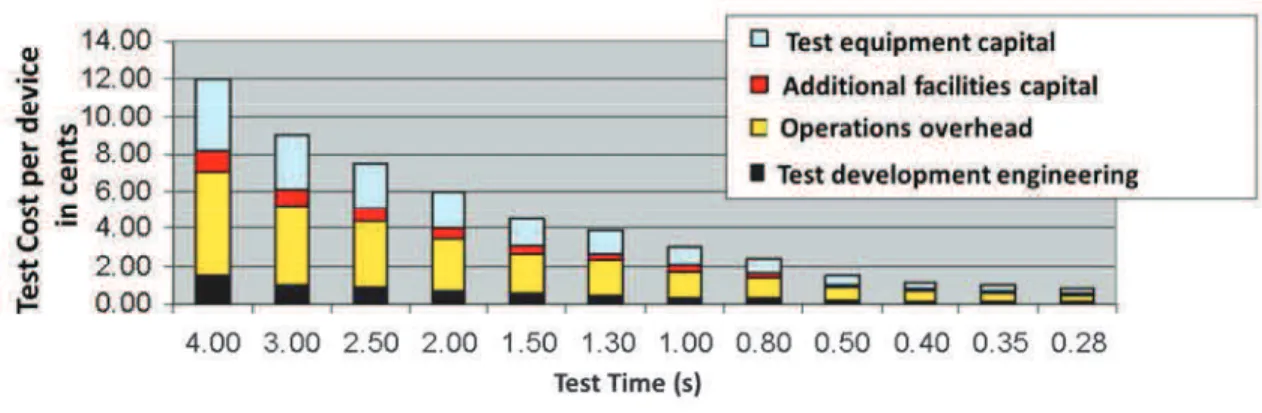
Given the large number of manufactured devise, typically several million per year, the test cost becomes very important criterion. The cost of a test solution results from many factors: test equipment capital, additional facilities capital (Handler, RF probes, etc.), operations overhead (operator, maintenance, building, etc.), Test development engineering [7] [8].
Fig. 2 emphasizes the relative importance of the test time on the overall test cost per
device. The cost factors associated with testing a device at various test times are shown. Note that the primary contributor to the device test cost is the operations overhead cost followed by the test system capital cost.
I
Fig. 2: Test cost versus test time.
According to this model the test time play a significant role to reduce the overall test cost per device. A total test time of 330ms leads to a one-cent-per-device total test cost. Based on the above observation, an RF IC test system is needed that could achieve a 300 ms (or less) per device test time to reach the targeted one-cent-per-device test cost. How to accomplish these two factors play a significant role starting with the hardware cost and then test time reduction.
Fig. 3: ATE cost increase with additional added features
The Fig. 3 shows the cost test equipment capital increase with adding additional features. Regarding to Fig. 2 and Fig. 3 RF devices have the highest test cost among all the types of circuits. This is due to the higher cost of the RF test features. This is a real obstacle for developing test solutions with a reduced cost per device. However, several techniques have been developed to relax the equipment constraints. The strategies presented in this chapter and in the next ones aim at reducing the amount due to the test equipment.
J
Concerning the test time, there are two main contributors: the time for the test program to run (which is linked to the time needed to set and operate each test) and how fast can the handler move the parts between the bins and the socket or move the wafer. This work focuses on the first contributor. One way to reduce the program test time is to simplify the test measurement required such as converting a test signal to a DC parameter instead of digitizing it. Further in this chapter, techniques for test time reduction and equipment cost reduction will be presented.
I.3
Analog/RF ICs testing specificity
I.3.1 Faults in analog/RF ICs
Faults in analog/RF ICs could be classified into two main categories: Catastrophic faults and parametric faults. Catastrophic faults (i.e. hard impact in the circuit) include generally shorts between nodes, open nodes and other hard changes in a circuit. Parametric faults (i.e. soft impacts in the circuit) are faults that do not affect the connectivity of the circuit; those are, for the most, variations of the dimensions of transistors and passive components due to a not well controlled technology process. Moreover, the parametric faults are further categorized into global and local faults. The first one occurs when all active or passive area in the device are impacted while the second occurs only when these areas are affected locally in the circuit. Global defects usually result from fluctuation in the manufacturing environment, such as a systematic misalignment of masks or a problem which systematically affects the active areas of the transistors. The variation of manufacturing environment can also lead to local defects. In this case, it is not a systematic variation but a local variation generating slight random differences between two adjacent components: this is called mismatch. Other typical example of a local defect is constituted by a dust particle on a lithographic mask producing a disparity such as a local variation in the ratio of a transistor.
I.3.2 Analog/RF ICs test: current practice
Usually, catastrophic faults are easy to detect. In this case the device has a severe dysfunction or it simply does not work. A simple continuity test is often enough to identify defective devices including this type of fault. In addition, defect models modeling shorts and opens in the circuit can be used to primary eliminate this kind of faulty circuits. The most problematic thing is how to detect devices including parametric faults. Insofar as the parametric faults affect the performance of the circuit, the device passes the continuity test
CK
and there are no reliable fault models that can detect the faults. The only way to detect the devices affected by the parametric faults is to measure the performance of the circuits and to compare them to those defined in its datasheet.
In the context of analog/RF ICs the specification test is usually reserved to the final test (i.e. packaged device). For many years, the wafer sort is based on decimating devices only including catastrophic faults. As a result there was limited ability to reduce overall test costs. Another problematic fact that with novel IC integration methods like SiP (System in Package) and 3D the industrials need for KGD (known good die) to develop reliable and cost efficient processes. The issue of package scrap is more problematic with these technologies. For the
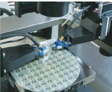
RF devices, KGD is synonym of specification test which performance of each device is measured. Fig. 4 shows an example of wafer level RF IC test.
Fig. 4: Wafer-level RF IC test (RF prob)
It is clear that wafer level test in this case is very costly due to the need of expensive equipment that avoids the possibility for multi-site testing.
During many years test engineers should choose between two strategies for RF IC testing. The first favor a cost optimized test solution for which only basic tests are performed at wafer level and a specification oriented test is performed once the devices are packaged. Note that this strategy leads to high scrap and does not suite advanced IC integration technologies like SiP and 3D. The second strategy favors a high quality test solution which is a costly and complex solution due to RF equipment needed to perform a specification based test at wafer level.
CC
In the following some techniques for RF IC test cost reduction are discussed. Some of these techniques use the IC resources to relax the constraints on tester equipment. Others try at time to optimize test time and relax tester constraints by using DC stimulus.
I.4
-This section presents a state-of-the-art of strategies proposed in the literature to deal with the test cost reduction of the analog and RF circuits.
I.4.1 Integrated test solution
A classical approach to reduce the equipment cost required for the test procedure, is to embed all or a part of the test resources into the circuit itself. This approach is known as Design for Testability (DfT) or Built-In Self-Test (BIST) in case of self-testing. Fig. 5 shows the principle of the integrated test.
Fig. 5: Principle of integrated test solution
These techniques either directly measure the circuit performance on-chip or produce a signature that has strong correlation to the “health” of the circuit. To offer self-test capability, the BIST circuitry, which comprises a signal generator and a response analyzer, should be more robust than the DUT. These techniques imply adding additional circuitry that can dramatically increase the device area. In the context of small devices like Low Noise Amplifier (LNA), mixer or Power Amplifier (PA) these techniques are not efficient due to the amount of added area for test resources. Contrariwise, they could be very interesting test solution in the context of complex circuit like SoC and SiP systems which digital resources of the device could be used for the RF front ends test.
C7
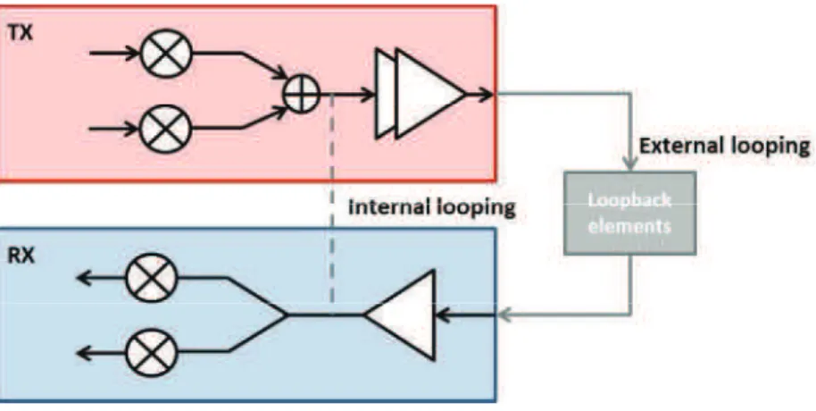
I.4.2 Loopback testing
The loopback testing is a low-cost solution for testing RF frontend modules and systems. Since the RF emitter and the receiver are integrated in the same device they are configured to test each other, the requirement for high-performance testers is alleviated [9]. The following figure shows the principle of the loopback testing.
Fig. 6: Principle of the loopback testing
Actually, the loopback testing is a system-oriented strategy to the extent that we are interested in evaluating the performance of the entire system and not to evaluate the performance of each RF block. The main advantages of this approach are on the one hand, the relaxed constraints on the test equipment necessary since the application and analysis of test signals are in baseband domain. Secondly, the test time is reduced since the whole system is tested once [10]. However, this approach suffers from limited test coverage [11] and requires careful design elements inserted in the system to perform the loopback [12] [13].
I.4.3 Indirect testing
Also called alternate testing, the purpose of this strategy is to relax constraints on the number and complexity of industrial test configurations needed to perform the RF parameters evaluation. Instead of directly measuring the circuit performances, the approach predicts them based on a set of DUT signatures that are captured from cheaper and simpler test setups and measurements. As presented by the Fig. 7, the underlying idea of indirect testing is that process variations that affect the conventional performance parameters of the device also affect non-conventional low-cost indirect parameters in the same way. If the correlation between the indirect parameter space and the performance parameter space can be established, then specifications may be verified using only the low-cost indirect signatures. Unfortunately
CD
the relation between these two sets of parameters is complex and cannot be simply identified with an analytic function. The solution commonly implemented uses the computing power of machine-learning algorithms.
Fig. 7: Underlying idea of indirect testing.
The indirect test principle is split into two sequential steps, namely training and production testing phases. The underlying idea is to learn during the training phase the unknown dependency between the low-cost indirect parameters and the conventional test ones. For this, both the specification tests and the low-cost measurements are performed on a training set of device instances. The mapping derived from the training phase is then used during the production testing phase, in which only the low-cost indirect measurements are performed.
The indirect testing is an interesting test solution for both package and wafer test levels. The non-complex indirect measurements are perfect for the wafer level test. Two main directions are explored for the implementation of the indirect testing, i.e. classification-oriented strategy [14] [15] [16] [17] [18] or prediction-classification-oriented strategy [5] [19] [20] [21].
A. Classification-oriented strategy
As illustrated by the Fig. 8 in the first direction, the Training Set (TS) is used to derive decision boundaries that separate nominal and faulty circuits in the low-cost indirect measurement space (specification tolerance limits are therefore part of the learning
Rsheet (Ohm/Seq) # Vth (V) # Tox (Å) # Gain(dB) # Good Bad Bad IP3(dB) # Good Bad Bad Process Variations
Performance Parameters Low-cost Indirect Parameters
Time (s) Vdc
Time (s) Idc
CE
algorithm). The objective is actually to perform the classification of each circuit as a good circuit or a faulty circuit, but without predicting its individual performance parameters.
Fig. 8: Classification oriented Indirect Testing
B. Specification prediction-oriented strategy
As illustrated by the Fig. 9 in the second variant, the training set is used to derive functions that map the low-cost indirect measurements to the performance parameters (typically using statistical regression models). The objective is actually to predict the individual performance parameters of the device; subsequent test decisions can then be taken by comparing predicted values to specification tolerance limits
Fig. 9: Prediction oriented Indirect Testing
The main advantage of this strategy is that it provides a prediction of the individual performance parameters. This information can then be used to monitor possible shift in process manufacturing, adjust test limits during production phase if necessary, or perform
Indirect low-cost measurements New
device Process through
learned decision boundaries
Pass/fail decision
CLASSIFICATION-ORIENTED ALTERNATE TESTING
Spec1 tolerance limits
TRAINING PHASE
PRODUCTION TESTING PHASE
Data from training set of devices Learn decision boundaries on indirect meas. Indirect low-cost measurements Analog/RF performance measurements Indirect low-cost measurements Data from training set of devices New
device Process through
built regression models Specs prediction Build regression model for Spec1 Indirect low-cost measurements Analog/RF performance measurements
PREDICTION-ORIENTED ALTERNATE TESTING TRAINING PHASE
CF
multi-binning. Because of these significant advantages of prediction-oriented approach on classification-oriented one, it is decided to focus improvement efforts on this approach. During next chapter this variant of the indirect testing will be studied in details.
Note that in case of DC-based indirect measurement this technique is practically suitable for wafer level testing.
C. Spatial correlation based testing
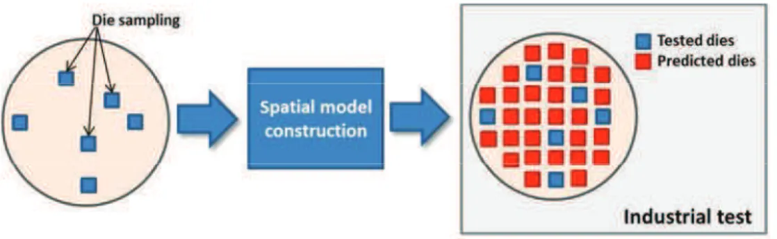
Another type of exploiting correlation in analog RF IC testing is the spatial correlation based approach. In this case, contrary to the indirect test approach, costly speci!cation tests are not completely eliminated. Instead, they are only performed on a sparse subset of die on each wafer and, subsequently, used to build a spatial model, which is then used to predict performances at unobserved die locations in the wafer. The assumption made is that during the manufacturing process the neighboring dies are affected in the same way. Knowing the value of the performance of a die, we can predict the performance of its nearest neighbors. The Fig. 10 shows the synopsis of the spatial correlation based testing.
Fig. 10: Wafer level test cost reduction based on spatial correlation.
Several works investigate methods to develop variability decomposition method for spatial modeling. In [22] authors estimate the spatial wafer measurements using Expectation Maximization (EM) algorithm. The idea assumes that data is governed by a multivariate normal distribution. In case that the assumption is not true the authors use the Box-Cox transformation. Another way to model the spatial variation is the Virtual Probe (VP) which uses a Discrete Cosine Transform (DCT) to define the model [22]. Similarly, Gaussian Process (GP) models based on Generalized Least Square !tting can be used for the spatial interpolation of manufacturing data [23].
We note that good accuracy of spatial model is not usually guaranteed. In [24], authors combine the indirect testing with the spatial correlation for enhanced accuracy models.
CG
I.5
Conclusion
The importance of developing high quality and cheaper IC is highlighted by the interest of semiconductor industrials to develop leading test techniques. Contrary to digital circuits the test of the RF IC is one of the problematic issues in semiconductors industry development. Due to the high cost of the RF IC test equipment. The need to develop cost efficient test strategies for the RF IC is expressed.
In this chapter, after introducing the general context, a brief recall of the specificity of the industrial test in particular RF IC test is presented. Factors impacting the cost of a given test solution are identified. It is pointed that the cost of the test solution can be easily reduced by acting on two factors: First, the test equipment capital, by relaxing its constraints using resources imbedded in the DUT for example. Second, test time which is reduced using low frequency and DC measurements. Then techniques allowing a cost reduced RF IC testing are presented. Emphasis is put in indirect testing which is a promising strategy to develop an extreme low cost RF test solution and a wafer-level as package-level suitable test solution. In the next chapter a case of study of the prediction-based indirect testing will be analyzed.
CI
II.1
Introduction
In this chapter, the author investigates the second approach of the indirect test, namely prediction-oriented indirect test. In literature, there are some contributions [4] [6] [25] [26]based on this approach; authors use different test vehicles, different regression algorithms and different efficiency metrics to implement and validate their test strategies. So, the analysis and the comparison between these works are not evident. The objective of this chapter is to analyze the efficiency of the classical implementation of prediction-oriented indirect testing and to define the framework that will be used all along the manuscript to implement and validate our proposals.
The first part of the chapter gives a brief overview of the classical implementation of prediction-oriented indirect testing and introduces the DC-based strategy we intend to use. The test vehicles that will be used for evaluation are then described and the RF parameters intended to be tested are defined. In the second part of the chapter, preliminary experiments are presented and discussed to compare some regression-fitting algorithms applied in the field of prediction-based indirect test and weaknesses of the conventional implementation scheme will be highlighted.
CJ
II.2
-The implementation of indirect testing involves two sequential phases, namely model building and production testing phases as illustrated in the Fig. 11.
(a) Model building phase
(b) Production testing phase
Fig. 11: Indirect Test: classical implementation
The first phase involves two steps: the training and the validation steps. During the training step, the unknown dependency between the low-cost indirect parameters and the
RF performances is studied. For this, both specification tests and low-cost measurements are performed on a Training Set (TS) of devices and a machine-learning algorithm is used to build regression models that map the indirect measurements to the RF performances. There is then a validation step in which the accuracy of the derived models is evaluated
7K
by comparing specification values predicted using the models to actual specification values. This evaluation is performed on a Validation Set (VS) of devices different from the training set, but for which both indirect measurements and specification measurements are available.
When the prediction accuracy meets the expectations, the production testing phase can start. In this phase, only the low-cost indirect measurements are performed and RF specifications are predicted using models developed in the previous phase.
II.3
DC-based indirect test strategy
A cornerstone of the efficient implementation of the indirect test approach is to find low-cost indirect measurements that are well correlated with the RF parameters. Chatterjee et al. first introduced this approach to reduce test time for analog and mixed-signal devices. They use stimuli like multi-tone or Piece Wise Linear (PWL) mixed-signals and they capture the transient output response in order to extract relevant signatures used to feed the machine-learning algorithm. The key idea to reduce test time is to predict all the circuit specifications from a single acquisition with a carefully optimized test stimulus, instead of using different dedicated test setups as usually required by conventional specification measurements. Regarding the use of the indirect test approach for RF circuits, the objective is also to relax the constraints on the required ATE resources, besides test time optimization. In this context, an attractive approach is to implement the indirect test strategy using only DC measurements. In this case, expensive RF options can be omitted from the ATE and only cheap DC resources are exploited. In addition because
DC resources are usually widely available on a standard ATE, multi-site testing can be implemented to further reduce test time.
In this work, all experiments will be performed considering this DC-based indirect test strategy. Different types of DC measurements will be exploited including DC voltages on internal nodes (the circuit has to be equipped with simple DfT allowing to probe some internal nodes), standard DC measurements classically performed during production test (e.g. power supply current measurement, reference biasing voltage measurement…) or DC signatures extracted from embedded process sensors (e.g. MIM1 capacitor, dummy transistors…). These measurements combined to different power, bias and temperature conditions could provide a huge number of indirect measurement 1
7C
candidates. The choice of a pertinent set of IMs for predicting the RF specifications is an area of research that will be discussed in the next chapter.
II.4
In this section, we first present the two circuits from NXP Semiconductors that will be used as test vehicles: a Low-Noise Amplifier (LNA) and a Power Amplifier (PA). We then define the RF parameters to be predicted with the indirect test approach, together with the conventional method to measure these parameters.
II.4.1 The Low Noise Amplifier
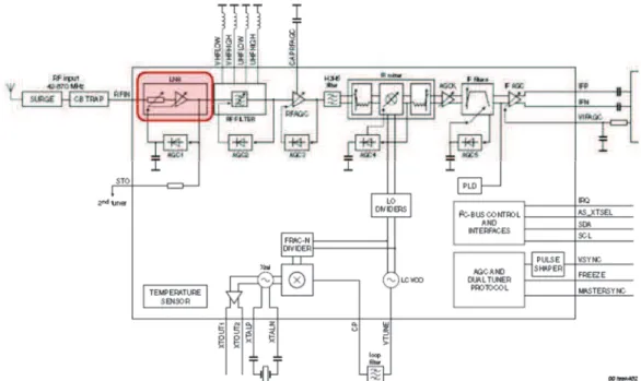
The first test vehicle is a wideband variable-gain Low-Noise Amplifier (LNA) integrated in a hybrid tuner for analog and digital TV. Fig. 12 shows the block diagram of the tuner where the LNA block is highlighted in red. This test vehicle has four different operating modes corresponding to four different gain settings: 6dB, 9dB, 12dB and 15dB.
Fig. 12: Block diagram of the tuner
The objective is to estimate three different RF performances, namely Gain, Noise Figure (NF), and the 3rd order Intercept Point (IP3) under the different operating modes,
there are therefore twelve RF performances to predict.
This device is equipped with an analog bus that allows probing of six different internal nodes. DC voltages on these internal nodes are obvious IM candidates together
77
with DC voltage measurement on the conventional RF output. These measurements can be performed for the different functional modes of the device and for different values of power supply. Here five different values of the power supply are considered ranging from
3.0V to 3.6V (typical power supply voltage is 3.3V). So the final set of IM candidates is composed of 120 elements. For this device, both RF performance measurements and indirect measurements are obtained from simulation of a population of 500 devices generated through Monte-Carlo simulations.
II.4.2 Power Amplifier
The second test vehicle is a Power Amplifier (PA) with high linearity (see Fig. 13). This PA is intended to be used in telecommunication applications. For this test vehicle, we have a large set of experimental (tester) data measured on 10,000 devices, which includes 37 low-cost Indirect Measurements (IM) based on standard DC test and 2 RF performance measurements, namely the 1-dB compression point (CP1) and the third order intercept point (IP3).
Fig. 13: Block diagram of the PA
II.4.3 RF Parameters
II.4.3.1. Gain
In RF devices, the power gain is more significant parameter than the voltage gain. The most common definition of power gain is the so-called transducer gain G defined by:
7D
Eq. (3.1)
where Pload is the power at the load and Pavailable is the power available from the source.
This definition assumes that matching at the input and the output ports of the DUT is optimized and that reflections at the input and the load could be neglected. However the gain exhibits a frequency-dependent behavior that should be characterized over all the functional frequency range of the device. Usually a network or spectrum analyzer equipment is used for this gain frequency response measurement. In volume production test, this technique is not preferred due to test cost and time considerations. Thus, in this context the gain is only evaluated at a given frequency in the functional range and only
RF signal generator and power meter are required for the gain measurement.
II.4.3.2. Noise Figure (NF)
In telecommunication systems, especially those dealing with very weak signals, the signal-to-noise ratio (SNR) at the system output is a major criterion. The noise added by the system components might tend to obscure the useful signals and dramatically degrade
SNR. The figure of merit that gives a measurable and objective qualification of this degradation is the Noise Figure (NF). Fig. 14 illustrates the degradation. The basic definition of NF is the ratio of SNRin at the input and the SNRout at the output [27].
!
"# Eq. (3.2)
There are two main techniques for the NF measurement: the “Y-factor” technique and the “Cold-source” technique [28] [29]. For the first technique (i.e. Y-factor) a noise source and two power measurements are required to calculate the NF. The first measurement is made with the noise source in its cold state: noise diode is off. Then the second measurement is made with the noise source in the hot state: noise diode is on. From these two measurements, and from knowing the ENR7 values of the noise source, the NF can be calculated.
2
7E
Fig. 14: SNR degradation of a signal passing through a semiconductor device
The cold-source technique consists in measuring the output power with the DUT placed at room temperature. The measured noise is the combination of the amplified input noise and the noise added by the device itself. If the amplification gain is accurately known, then the amplified input noise can be subtracted from the measurement, giving only the noise contribution of the DUT. From this the noise figure can be calculated. For this technique a vector network analyzer is required for doing measurements.
Note that for the two cited techniques, a calibration step is highly required to characterize and compensate the actual noise added by the circuitry of measurement equipment.
II.4.3.3. Gain Compression
The gain compression is a non-linear phenomenon due to the device saturation. In the linear region, when the input power increases, the output increases according to the device gain. As shown in Fig. 15, from a certain level of input the signal is not amplified as expected. This input level is said to be the compression point. Quite often, it is referred to the one-dB compression point (CP1) for amplifiers but two-dB or three-dB compression points could be defined for other devices or applications.
7F
Fig. 15: Definition of the 1-dB Compression Point
The measurement of the CP1 is often performed in two steps. As the device gain response is not the same over frequencies, the frequency at which the 1-dB gain compression first occurs is needed to be located. Then, a power sweep is applied to the device’s input. The gain compression can be observed when the input power is increased by 2dB while the output power increases by 1dB. Note that at least an RF signal generator and a power meter are required for doing measurements.
II.4.3.4. Third Order Intercept Point
The third order intercept point (IP3) is an important parameter that defines the distortion caused by the nonlinearity of the device. This point is usually defined as the intercept point between the theoretical gain characteristic and the interpolation of the third order distortion characteristic as illustrated in Fig. 16.
7G
The measurement of the 3rd order intercept point is divided into two groups: in-band and out-of-band measurements. In-band measurements are used when the tones are not attenuated by filtering through the cascade.
For example, intercept point for a power amplifier is generally done with 2 tones that exhibit the same power throughout the system. Out-of-band measurements are used when they are attenuated like filtering in an Intermediate Frequency (IF). In the case of our study, only in-band measurements will be done. For the in-band measurements two tones, $% and $& are created by two signal generators and combined before entering the
DUT.
Fig. 17: In-band Intermodulation Measurement
The intercept point is determined from the measured power level of the two tones and the power levels of the intermodulation tones on a spectrum analyzer as shown in the
Fig. 17. The Output third order Intercept Point (OIP3) is determined as follows:
'()* + ),-./ 01&2 Eq. (3.3)
The Input third order Intercept Point is deduced as:
7H
II.5
Benchmarking of some machine-learning
regression algorithms
There are several machine-learning algorithms used for regression mapping. In the field of indirect testing, people use different algorithms but they didn't discuss their choice in detail [5] [21]. In this section, we investigate the performance of four commonly-used machine-learning algorithms on a practical case study. The four algorithms are first briefly described. Then the case study is then presented. Finally results are analyzed and discussed.
II.5.1 Multiple Linear Regression
The most basic regression model consists in a linear relationship between the response variable to be evaluated (i.e. one analog/RF performance in our case) and one or more predictor variables (i.e. indirect measurements in particular case). The case of one predictor variable is called simple linear regression while for more than one predictor variable, it is called multiple linear regression. Given a dataset 6789 :8%9 :8&9 ; 9 :8<=
8>% of
N elements, where 7 is the response variable to be predicted and :%;< are the p predictor variables, the multiple linear model takes the form:
7 :? 0 @ Eq. (3.5) With 7 A B% C B D E : A F%% ; F% C G C F % ; F D E ? H ?I ?% C ? J E @ A@C% @ D
The ? vector is usually estimated using the least mean square estimator as follows:
?K L:,:MN%:,7 Eq. (3.6)
This equation assumes that :O: is invertible, which means that all variables are non-correlated. In the practical case of indirect test this assumption is not always verified, some measurements might be correlated.
7I
II.5.2 Multivariate Adaptive Regression Splines
The Multivariate Adaptive Regression Splines (MARS) [30] is a form of regression model presented for the first time by J. Friedman in [31]. This technique can be seen as an extension of the linear regressions that modeled automatically interactions between variables and nonlinearities. The model tries to express the dependence between one response variable 7 and one or more predictor variables :%;<, on given realizations (data) 6B89 F8%9 ; 9 F8<=%. The phenomenon that governs the data is presumed to be:
7 $L:M 0 @ Eq. (3.7)
The aim of algorithm is to use the data (learning technique) to build an estimated function $KL:M that can serve as a reasonable approximation to $L:M over the domain of the interest constituted by the predictors. The estimated function $KL:M is built from bilateral truncated functions of predictors having the following form where the summation is over the non-constant M terms of the model:
$KL:M ?I0 PR+>%?+Q+L:M Eq. (3.8)
This function is constituted by the term ?I the value of 7 where : L 9 ; 9 M and a weighted sum of one or many basis functionsQ+L:M. Each basis function is simply a hinge function and takes one of the two following forms:
A hinge function has the form ofSTUL 9 F V WM X STUL 9 W V FM. Where c is a constant, called the knot. The hinge function is often represented:
LF V WMY Z F V W O\]X \4^] _F [ W Eq.(3.9)
A product of two or more hinge functions which have the ability to model interactions between two or more predictors.
One might assume that only piecewise linear functions can be formed from hinge functions, but hinge functions can be multiplied together to form non-linear functions.
Note that the MARS model can treat classification problem as well as prediction problem. Therefore, it is used for both variants of indirect test, namely the classification-oriented test and the prediction-classification-oriented test.
7J
II.5.3 Artificial Neural Network
An Artificial Neural Network (ANN) is a mathematical model inspired by biological neural networks, which involves a network of simple processing elements (neurons) exhibiting complex global behavior determined by the connections between the processing elements and element parameters. Neural networks can be used for modeling complex relationships between inputs and outputs and they have been successfully implemented for prediction tasks related to statistical processes.
Fig. 18: Single Neuron
As presented in Fig. 18 the basic processing element of a neural network, i.e. the neuron, computes some function f of the weighted sum of its inputs, where f is usually named the activation function. Many activation functions could be used: linear, z-shape, hyperbolic tangent, threshold, etc.
7 $L3M 4O\ 3 P8 8F8 Eq. (3.10)
II.5.4 Regression Trees
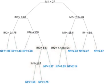
Decision trees can be used to create a model that predicts the value of a target variable 7 based on several input variables F%9 ; 9 F<. Each interior node corresponds to one of the input variables and each leaf represents a value of the target variable given the values of the input variables represented by the path from the root to the leaf. A tree can be "learned" by splitting the source set into subsets based on an attribute value test. This process is repeated on each derived subset in a recursive manner. The recursion is completed when the subset at a node has all the same value of the target variable, or when splitting no longer adds value to the predictions [32]. Fig. 19 illustrates the case of a
DK
regression tree built for the prediction of the NF performance based on 4 indirect measurements (IMi). Note that decision trees could fit with both variants of the indirect
test strategy: prediction-oriented and classification-oriented strategies.
Fig. 19: The regression tree
II.5.5 Test case definition
As previously mentioned, the choice of a given machine-learning algorithm is generally not discussed in the literature. In order to compare the performance of different algorithms, experiments have been performed on one case study that involves the prediction of the CP1 specification for the PA test vehicle. Note that for meaningful comparison, exactly the same training and validation data will be used for the four algorithms.
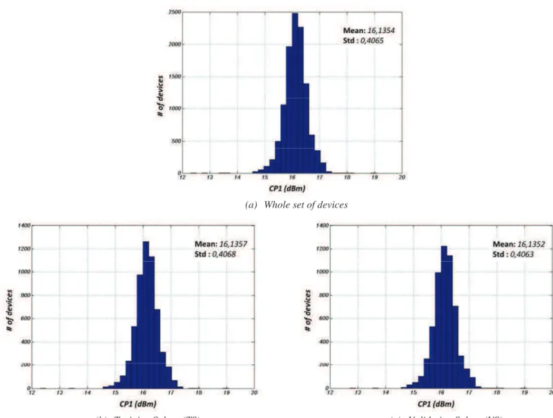
Practically, the experimental test data available from 10,000 devices are split into two subsets of 5,000 devices, one that will be used for training and the other for validation. A technique inspired from Latin Hypercube Sampling [33] [34] (LHS) is used to obtain two subsets with similar statistical properties regarding the CP1 specification, as illustrated in Fig. 20.
DC
(a) Whole set of devices
(b) Training Subset (TS) (c) Validation Subset (VS)
Fig. 20: Statistical properties of Training and Validation subsets regarding CP1
specification
Data from the 5,000 training devices are fed into the different machine-learning algorithms and corresponding regression models are built (models are built with the same set of 4 pre-selected IMs in this experience). These four models are then used to perform
CP1 prediction for the 5,000 other devices of the validation set. Efficiency of the different algorithms can be evaluated qualitatively by comparing correlation graphs, i.e. graphs that plot predicted CP1 values with respect to the actual CP1 value. The closer the points to the first bisector, the better the model accuracy is. Efficiency can also be evaluated quantitatively by computing the Mean Squared Error (MSE) metric defined by:
D7
`ab %P LB8>% 8 V Bc8M& Eq.(3.11)
where N is the number of devices, yi and i are the actual and predicted RF performances
of the ith device, respectively. The lower the MSE metric, the better the model accuracy is.
II.5.6 Results and discussion
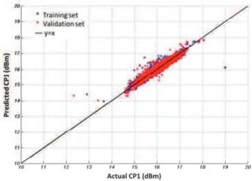
Fig. 21 gives the correlation graphs obtained with the four different regression
algorithms. For the sake of comparison, all graphs are presented with the same scale from 10 to 20dBm. It clearly appears that the regression models built using MARS, Regression tree (M5P) and ANN algorithms offer better performance than the model built using MLR algorithm, which could not fit the correlation between used IMs (i.e. predictors) and the
RF specification. So the linear model will be ruled out for the rest of the study.
From the qualitative analysis of these graphs, there is no significant difference between MARS, M5P and ANN algorithms. In the three cases, most of the devices are correctly predicted with a good accuracy. This is confirmed by computing the MSE metric associated to each model, which exhibits similar value:
`abdRe f gE `abdRh f iE `abde f i*
To further analyze the performance of these three regression algorithms, a more advanced evaluation is necessary. To do this, regression models are built for the three algorithms considering 1,000 different combinations of 3 IMs randomly chosen among the 37 low-cost IMs available for this case study. The MSE metric is then computed on both training and validation subsets, for each model and each regression algorithm.
DD
(a) Regression model built using MLR algorithm (b) Regression model built using MARS algorithm
(c) Regression model built using M5P algorithm (d) Regression model built using ANN algorithm
Fig. 21: Comparison of the correlation plots obtained
with 4 different regression algorithms
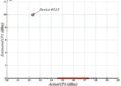
During this experiment, it sometimes happens that the estimation of the RF performance is aberrant for a particular model and a particular device of the validation subset. As an illustration, Fig. 22 shows the case of an aberrant CP1 prediction for one device (device number 513) with a predicted value around jfj %%klm , which of course never happens in real circuit. If this prediction is considered in the calculation of the MSE, it significantly affects the calculated value, which is fng*j &I for this example. If this aberrant prediction is removed for the computation, the non-biased value of the MSE is 0.0162, which corresponds to a realistic value of the MSE for this example. Consequently for a faithful comparison of the model accuracy achieved using the different regression algorithms and the different IM combinations, such aberrant
DE
predictions should be removed from the MSE calculation on the validation subset. Note that these aberrant predictions are easy to identify because they are totally out of the possible value range of the performance to be predicted (for the case of the CP1 performance, a realistic range of the possible predicted values is from 0dBm to 30dBm). We denote these predictions Out-Of-Range (OOR) predictions.
Fig. 22: Example of aberrant prediction for one particular device
All the results presented in the following are computed after removing the OOR predictions from the validation subset. Fig. 23 reports the MSE values corresponding to the 1,000 models built with different IM combinations, for the three different regression algorithms. In each graph, both the MSE calculated on the Training Subset (TS) and the
MSE calculated on the Validation Subset (VS) are provided. The MSE calculated on TS translates the ability of the model to accurately represent the relation that links the selected IMs to the RF specification for the considered training devices, while the MSE calculated on VS translates the ability of the model to accurately predict the value of the
RF specification from the selected IMs for new devices different from the training devices. So to ensure accurate performance prediction, a model should exhibit not only a low MSE value with respect to TS, but also an MSE value in the same range with respect to VS. Note that for the sake of clarity, models are sorted regarding their MSE computed on TS.
DF
(a) Models built with MARS algorithm (b) Models built with M5P algorithm
(c) Models built using ANN algorithm
Fig. 23: MSE variation over models built with different IM combinations
for different regression algorithms
Analyzing these results, a slight advantage appears for the MP5 regression algorithm regarding MSE values calculated on TS. However there is a significant discrepancy between MSE values calculated on TS and VS. In the same way for the ANN regression algorithm, a good MSE value on TS does not ensure a MSE value on VS in the same range. In contrast, the MARS regression algorithm appears much more robust since most of the models built with this algorithm give almost identical values for the MSE calculated on both TS and VS. For these reasons, the MARS algorithm will be chosen for regression model construction during the rest of the study.
DG
II.6
Limitations & bottleneck of the conventional
indirect test scheme
The main challenge of indirect test is the prediction confidence. The confidence is usually assimilated to two aspects: the first one is the model accuracy which is usually expressed in terms of average prediction error; the second one is the model robustness against anomalies which usually manifest themselves in the devices having a big prediction error. In the following some experiments which highlight the weaknesses of the classical implementation of the indirect test are presented.
II.6.1 Prediction confidence: flawed predictions
Many of the experiments reported in the literature on various devices demonstrate that very low average prediction error can be achieved. However, two main points limit the credit we can give to this good accuracy. First, low average prediction error does not guaranty low maximal prediction error, which is of crucial importance regarding the classification step where the predicted values are compared to the specification limits promised in the datasheet.
The maximal prediction error is defined as follows:
@+op qS<rs tP dB8>% 8 V Bc8d<
2
uvw%x8x dB8 V Bc8d Eq. (3.12)
Second, evaluation is usually performed on a small set of validation devices, typically ranging from few hundreds to one thousand instances, while the technique aims at predicting values on a large set of fabricated devices, typically one or several millions. So even if low maximal prediction error can be observed on the small validation set, there is no guarantee that the maximal prediction error will remain in the same order of magnitude when considering the large set of fabricated devices.
DH yz{ |}~• €• €•€• €• f j‚ f i ƒ„ …• …•…• …• f j† fjj‚ ƒ„
(a) TS: 1,000 devices ‡ VS: 1,000 devices
yz{ |}~• €• €•€• €• f j‚ f i ƒ„ …• …•…• …• f * †fˆj ƒ„ (b) TS: 1,000 devices ‡ VS: 5,000 devices yz{ |}~• €• €•€• €• f fiˆ ƒ„ …• …•…• …• f gfˆ ‚ ƒ„ (c) TS: 5,000 devices ‡ VS: 5,000 devices
Fig. 24: Illustration of prediction error for different sizes of TS and VS
To illustrate these points, some experiments have been performed on one case study that involves the prediction of the IIP3 specification for the PA test vehicle. Here again,
DI
the experimental test data available from 10,000 devices are split into two subsets of
5,000 devices with similar statistical properties, one used for training and the other for validation.
In the first experiment, 1,000 devices are chosen randomly from the TS to build prediction models based on triplets of IMs and the prediction accuracy is evaluated with
1,000 devices chosen randomly in the VS. As an illustration, Fig. 24.a presents an example of IIP3 prediction for one “good” model. In this case, `ab and @+op values calculated on both TS and VS give coherent results, with both low average and maximal prediction errors.
Then, in the second experiment, the number of the devices used for validation is increased to 5,000 devices, i.e. the obtained model is validated with a large VS. For most of the devices, the average prediction error is nearly preserved but we observe flawed predictions for some devices resulting in a large maximum prediction as illustrated in Fig.
24.b.
Such flawed predictions are usually attributed to the fact that the mapping obtained using finite-size TS is not fully representative of the actual complex mapping. So, in the third experiment, we use all the 5,000 devices of the TS to build the regression model and the prediction accuracy is evaluated using all the 5,000 devices of the VS. Unfortunately even with such a large training set, we still observe flawed predictions for some devices as illustrated in Fig. 24.c.
Note that one could reasonably think that these flawed predictions are due to some distinctive features of particular devices, for instance devices which are not consistent with the statistical distribution of manufactured devices. In this case, it would be possible to filter these devices prior to applying the alternate test procedure, as suggested in [15]. However this does not seem the case because different behaviors are observed depending on the model used to predict the performance, as illustrated in Fig. 25. Indeed even if both models are built with the same training set, flawed predictions are observed for devices 4,512 and 1,179 using model 1 while they are correctly predicted using model 2, and flawed prediction is observed for device 2,326 while it is correctly predicted using model 1.