HAL Id: hal-00776523
https://hal.archives-ouvertes.fr/hal-00776523
Submitted on 15 Jan 2013
HAL is a multi-disciplinary open access
archive for the deposit and dissemination of
sci-entific research documents, whether they are
pub-lished or not. The documents may come from
teaching and research institutions in France or
abroad, or from public or private research centers.
L’archive ouverte pluridisciplinaire HAL, est
destinée au dépôt et à la diffusion de documents
scientifiques de niveau recherche, publiés ou non,
émanant des établissements d’enseignement et de
recherche français ou étrangers, des laboratoires
publics ou privés.
Immunity Modeling of the LM2902 Operational
Amplifier
Sjoerd Op ’T Land, Frédéric Lafon, François de Daran, Frank Leferink,
M’Hamed Drissi, Mohamed Ramdani
To cite this version:
Sjoerd Op ’T Land, Frédéric Lafon, François de Daran, Frank Leferink, M’Hamed Drissi, et al..
Immunity Modeling of the LM2902 Operational Amplifier. EMC Europe 2010, 9th International
Symposium on EMC and 20th International Wroclaw Symposium on Electromagnetic Compatibility,
Sep 2010, Wroclaw, Poland. pp.1-4. �hal-00776523�
Immunity Modeling of the
LM2902 Operational Amplifier
Sjoerd Op ’t Land
∗, Fr´ed´eric Lafon
†, Franc¸ois de Daran
†, Frank Leferink
∗‡, M’hamed Drissi
§, Mohamed Ramdani
¶∗Chair of EMC
TE Group, University of Twente Enschede, The Netherlands Email: [email protected],
‡Technical Authority EMC
Thales Nederland Hengelo, The Netherlands Email: [email protected]
†Center of Electronics Excellence
Valeo VEES Cr´eteil, France
Email: [email protected], [email protected]
§Universit´e europ´eenne de Bretagne
IETR – INSA de Rennes Rennes, France Email: [email protected] ¶Department of Electronics ESEO – Lattis Angers, France Email: [email protected]
Abstract—Component models that predict functional failure are necessary for predicting the immunity of systems to electro-magnetic interference (EMI). A method to extract these models using measurements on integrated circuits (ICs) already exists. This measurement method for ICs with single-ended connections is extended, to include ICs with differential connections. The LM2902 op-amp is measured and modeled as a first case study.
Index Terms—immunity, integrated circuit, ICIM, DPI, mod-eling, differential connection, operational amplifier
I. INTRODUCTION
To reduce the number of prototyping cycles in the de-velopment of electronic products, we would like to predict the immunity of a product to electromagnetic interference (EMI) in an early stage. Specifically, we would like to be able to predict functional failure of a product under test using a circuit simulator like PSPICE. In order to be able to simulate the complete product, we first need component models that adequately predict functional failure. Models of passive components, including parasitics, are readily available [1], so we focus on Integrated Circuit (IC) models.
In earlier work, an immunity model was developed, in-cluding a measurement method to extract model parameters from various Integrated Circuits (ICs) with single-ended con-nections [2], [3]. This model and the corresponding method are summarized in section II. Then, an extended measurement method is proposed to characterize ICs with differential con-nections in section III. Characterization results of the LM2902 operational amplifier are presented and a behavioral model is suggested in section IV. In section V, we use this model to predict functional failure in simulation. These immunity predictions are then compared with measurements. Finally, we draw conclusions on the suitability of the proposed method and we indicate its current shortcomings (section VI).
II. STATE OF THEART
For components with single-ended connections, an im-munity model and a corresponding measurement method to extract the model parameters were developed in earlier work [1], and are briefly summarized below.
As suggested in [3], the model consists of a PDN (Passive Distribution Network) and an IB (Immunity Behavioral) part. The goal of this model is to describe the immunity of an IC under CW (Continuous Wave) disturbance. The failure mechanisms under CW disturbance or transient disturbance are in general quite different. This leads to different model structures and therefore, we do not try to obtain one model to describe the immunity to both types of disturbance.
The first part of the model, the PDN, is a linear circuit that describes the propagation of power. Regarding the kind of disturbance considered for this model (only a few watts of forward power in a DPI (Direct Power Injection) test configuration [4]), nonlinearities on the input and transfer impedances are generally quite negligible [2]. This observation leads us to use an S-parameter description to characterize and model an integrated circuit. This approach is compliant with typical end user constraints, who need to consider an IC as a black box. The S-parameters can be measured using a Vector Network Analyzer (VNA).
The second part of the model is the IB, and [2] suggests that the immunity of an IC is directly linked to a transmitted power threshold. This threshold power can be extracted by a DPI experiment [4] consisting in injecting disturbances directly on a pin of an IC in a controlled environment. For each frequency, the injected forward power is increased until the IC fails. This failure threshold power as function of the frequency is called the DPI performance. (The essence of the DPI measurement setup is given in Figure 1.) From the forward power threshold
Directional Coupler Amplifier RF Source PCB DC Signal Trace Bias Tee Coupling Capacitor IC Under Test Pforward Preflected P P
Figure 1. Typical DPI test setup as defined in IEC 62132-4 for single pin injection. [4]
thus found, the transmitted power threshold is extracted by means of simulation as developed in [2], [5].
With these measurements (S-parameters and DPI perfor-mance), we obtain a model that is able to predict the propaga-tion of a disturbance until the IC inputs (reflecpropaga-tion coefficients) and through the IC (transmission coefficients). This allows us to compute the total transmitted power to the IC in any configuration and to compare it to the threshold transmitted power available in the model.
This approach was successfully applied for the immunity prediction of various IC families, such as logic gates, LIN transceivers, MOSFETs, transistors and LDOs. It is interesting to note that the transmitted power seems to be a generally valid electrical criterion to describe the immunity of an IC.
III. MEASUREMENTSETUP
The extension of the transmitted power criterion to devices with differential connections is not obvious. For example, should the powers transmitted to the + and – inputs simply be added? Or does only the differential power matter? To find out, we develop a test setup that allows us to inject a variety of signals. Afterwards, we will evaluate whether or not we can describe the failure with a transmitted power threshold.
We choose to start with a case study on an LM2902 opera-tional amplifier. From practical experience, we know that this op-amp converts high-frequency EMI to a DC offset voltage at its output. Depending on the application, a certain output offset voltage will cause functional failure of the product.
As will be discussed in section IV and as is pointed out in [6], the output offset of op-amps under a Continuous
Wave (CW) disturbance is a function of vcm, vdm and φcmdm,
being the common-mode disturbance voltage amplitude, the differential-mode disturbance voltage amplitude and the phase shift between common-mode and differential-mode distur-bance, respectively. In order to properly characterize this kind of IC, we need to develop a test setup that allows us to
independently control vcm, vdmand φcmdm, since the traditional
DPI test method does not allow this.
To generate two Direct Power Injection (DPI) signals, one for the + input and one for the – input of the LM2902
op-amp that have a controllable φcmdm, the common-mode and
differential-mode signals need to be coherent. Consequently,
90º 0º 90º 0º – + LM2902 LTC5598 LTC5598 DPI+ DPI– V
Figure 2. Principle of the differential disturbance injector, which uses two quadrature modulators. The biasing circuitry of the LM2902 is not shown.
DPI+ and DPI– should have a fixed phase relationship. There-fore, a single CW source is used to derive both DPI+ and DPI– disturbance signals from (cf. Figure 2). Two quadrature mixers derive a sine and a cosine from this single source. Using four DC-coupled control signals, the amount of sine and cosine in both DPI+ and DPI– disturbance signals can be
individually controlled, to generate every combination of vcm,
vdm and φcmdm. Finally, the voltage offset at the output of the
LM2902 is measured.
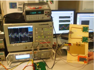
This measurement principle was realized using two LTC5598 quadrature mixers on DC1455 demonstration boards, generously provided by Linear Technology. An IFB 2023 RF signal generator was used as CW source, followed by a custom resistive power splitter. An Agilent 34401 multimeter was used to measure the output offset voltage. For monitoring purposes, a Tektronics TDS5104B oscilloscope was connected to the DPI+ and DPI– nodes. The generic DPI PCB developed in [2] was used to mount the LM2902 on, and to provide its biasing circuitry. The resulting setup is schematically depicted in Figure 3, the realization in Figure 4.
A PC calculates the modulator control voltages from the
wanted vcm, vdm and φcmdm and drives the D/A converter to
apply these voltages to the modulators.
Currently, we are not able to control the modulators very accurately, so we use the oscilloscope to measure the actually
applied vcm, vdm and φcmdm. There is an important
disadvan-tage to this solution, however: the input impedance of the LM2902 pins is not, in general, 50 Ω. As a result, for high frequencies, there will be standing waves on the transmission line from the modulator to the IC. Although the oscilloscope is placed close to the IC, there will be a discrepancy between the voltage measured by the oscilloscope and the actual voltage on the LM2902 pin. The connecting cable is 1 m length, so at 100 MHz, half a wavelength fits in the cable. Somewhere around this frequency, we should start to be critical toward
LISN LISN +12.5V RF Generator GPIB CH1 +5V LISN Multimeter GPIB Oscilloscope GPIB CH2 D/A Converter Quadrature Modulator Quadrature Modulator Power Splitter
(I/Q control voltages)
2
9
0
2
GPIB
Figure 3. Schematic measurement setup, used to characterize the LM2902 op-amp. A PC (not depicted) controls the RF generator and D/A converter, and reads measurements from the multimeter and oscilloscope. LISNs (Line Impedance Stabilizer Networks) are included, to have a defined and known power supply.
Figure 4. Realized measurement setup. The PCB at the bottom is used to mount the LM2902, the board at the right contains the power splitter and the two quadrature modulators. The PC is running the LabView control software.
the oscilloscope’s readings. The modulators, however, work well up to 1.6 GHz, so if we would improve the modulator control, thereby obsolescing the oscilloscope, we could extend the frequency range up to 1.6 GHz.
For low frequencies, for yet unknown reasons, there seems to be an imbalance between the sine and cosine components generated by the modulators. We compensate for this effect in software, but this negatively affects accuracy for low fre-quencies. Therefore, the current setup is limited to frequencies above 5 MHz.
To sum up, we have developed an injection setup that allows us to inject a CW disturbance into a differential input. We can
individually control vcm, vdm and φcmdm. The CW frequency
can be set between 5 and 100 MHz.
-1,2 -1 -0,8 -0,6 -0,4 -0,2 0 0,2 0,4 0,6 0,8 1 1,2 -180 -135 -90 -45 0 45 90 135 180 fcmdm (degrees) V offs et (V dc ) -0,12 -0,1 -0,08 -0,06 -0,04 -0,02 0 0,02 0,04 0,06 0,08 0,1 0,12 A m pl itude (V rm s) Voffset (Vdc) Vcm (Vrms) Vdm (Vrms) Voffset,out(Vdc) Vof fset,out (V dc ) vcm(Vrms) vdm(Vrms) Amplitude (V rms ) φcmdm(◦)
Figure 5. Measured output offset voltage, while sweeping φcmdmand trying
to keep vcmand vdm constant at f = 60 MHz.
IV. CHARACTERIZATIONRESULTS
In the first sweep that we perform, we try to keep vcmand
vdm constant and sweep φcmdm, while the CW frequency is
60 MHz. The result is plotted in Figure 5.
Note that the injection setup succeeds somewhat in keeping
vcm, vdm constant, albeit not perfect (60 mVrms± 10 mVrms).
Furthermore, the main observation is that the output offset
voltage is a shifted sinusoid as function of φcmdm. This might
correspond to the analytical prediction of [6, Eq. 12 and 13]:
Voffset,in=
gpvcmvdm|Y(jω)|
2gm
cos(φcmdm+6 Y(jω)), (1)
where gp, gmand Y(jω) are transistor and technology
parame-ters. Voffset,inis the equivalent RF-induced input offset voltage.
In closed loop op-amp configurations, this input offset appears attenuated at the output, depending on the loop gain. Given a certain loop gain (op-amp open loop gain times feedback gain), and a certain disturbance frequency, the output offset
voltage should also be a sinusoid as function of φcmdm.
While comparing our measurements (Figure 5) with the model of (1), we notice two significant differences. First and foremost, the average output offset voltage is nonzero, while
the average of a cosine is zero. Second, 6 Y(jω) should be
between 90◦and 0◦[6, Eq. 8]. Most probably, there is a phase
reversal somewhere in our setup with respect to the analysis of [6], although we have not yet been able to find it.
Treating the op-amp with a fixed feedback network as a black box, we can state the following anonymous behavioral model:
Voffset,out= vcmvdm[F(ω) cos(φcmdm+ G(ω)) − H(ω)] , (2) where F, G and H are (real) fit-parameters. Note that we added H to describe the currently unexplained nonzero average offset. We can test the hypothesis that (2) constitutes a good
model, by performing a φcmdm-sweep with different vcm/vdm
combinations. We fit an F, G and H to the results of each sweep, and we check that F, G and especially H stay about constant. The results of this experiment are enumerated in Table I.
For vcm/vdmratios close to 1, H (as defined in (2)) seems to
Table I
FITF, GANDHFOR DIFFERENTvCM/vDM
COMBINATIONS INφCMDMSWEEPS AT60 MHZ.
Stimulus Fit parameters
vcm vdm F G H no. (mVp) (mVp) (Vp−1) (◦) (Vp−1) 1. 11.9 12.1 131.9 12.2 5.50 2. 11.9 12.2 131.3 11.5 5.46 3. 80.4 82.0 137.4 11.1 5.35 4. 80.0 55.1 142.3 10.8 5.04 5. 79.8 29.2 138.4 12.5 11.85 6. 53.3 80.8 141.5 11.6 4.66 7. 27.5 79.8 137.6 12.3 7.60 0 15 30 45
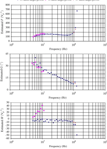
1,E+06 1,E+07 1,E+08 1,E+09 Frequency (Hz) E st im at ed G (º) -60 -50 -40 -30 -20 -10 0 10 20 30 40 50
1,E+06 1,E+07 1,E+08 1,E+09 Frequency (Hz) E st im at ed H (1/ V p) 0 100 200 300 400 500 600 700 800
1,E+06 1,E+07 1,E+08 1,E+09 Frequency (Hz) E st im at ed F (1/ V p)
-33 dBm target power -41 dBm target power -17 dBm target power
106 107 108 109 106 107 108 109 106 107 108 109 Estimated F (V − 1 p ) Estimated H (V − 1 p ) Estimated G ( ◦)
Figure 6. Fitted F, G and H to φcmdm-sweeps at different frequencies and
different forward injection powers.
sweep 5-7). To first order approximation, however, H suffices (cf. sweep 1-4). As for F and G, the results suggest being
reproducible within±5 Vp−1 and±1◦, respectively.
Finally, we perform φcmdm sweeps among a range of
fre-quencies, to determine F(ω), G(ω) and H(ω), see Figure 6.
In these sweeps, vcm= vdm. F and G are relatively smooth as
function of the frequency, but H is quite noisy and apparently, dependent on the forward injection power.
-35 -30 -25 -20 -15 -10 -5 0 5
1,00E+06 1,00E+07 1,00E+08 1,00E+09 Frequency (Hz) F ai lure pow er (dBm ) simulation (FGH) measurement 106 107 108 109 simulation (FGH) – +
Figure 7. DPI+ performance of the LM2902, simulated and measured.
-35 -30 -25 -20 -15 -10 -5 0 5
1,00E+06 1,00E+07 1,00E+08 1,00E+09 Frequency (Hz) F ai lure pow er (dBm )
simulation (FGH) simulation (FG) measurement
106 107
108 109
simulation (FGH) simulation (FG)
– +
Figure 8. DPI+ performance of the LM2902 with 100 pF between + and –. Simulated using (F, G, H)-parameters (thick curve) and simulated with only (F, G)-parameters (thin curve).
V. SIMULATION VS. MEASUREMENTS
Now that we have a model (2) and now that we have measured the model parameters (Figure 6), we would like actually to perform a product simulation. For example, what is the DPI performance of the LM2902, when we inject only on the + input? How does this DPI performance change (improve?) if we add a 100 pF capacitor between the + and – inputs?
As with the ICIM (Integrated Circuit Immunity Model) method described in section II, we characterize the LM2902 by measuring its S-parameters with a Vector Network Analyzer (VNA). These are transferred in PSPICE, using [7]. This allows us to predict the voltages on all IC pins, given a 0 dBm disturbance injected on one of the pins. Simultaneously, the simulator looks up the measured F, G and H as voltages for each frequency. Using Allegro AMS Simulator macros, we calculate the forward injection power that would cause the failure output voltage offset. Note that the failure output voltage offset must be chosen in the macros. This means that the same model can be used for applications requiring different maximum output offsets.
First, we simulated the DPI performance of the LM2902, for injection on the plus pin, only with the op-amp and its biasing circuitry. The result is plotted in Figure 7, together with a DPI
measurement. The failure criterion was |Voffset,out| > 50 mV. Another pair of simulations and measurement was performed, with a 100 pF capacitor between + and – pins (Figure 8). This simulation was carried out with and without H, to assess the improvement of the model by adding H.
The simulation of the clean configuration (Figure 7) matches quite well with measurements (±2 dB until 100 MHz). We suppose the deviation close to 125 MHz to be caused by the standing wave problems during parameter estimation. Furthermore, we note ripples in the simulation results that might be caused by nonsystematic errors during parameter estimation measurements.
The simulation of the LM2902 with a 100 pF capacitor inserted, has bigger deviations (cf. Figure 8). The argument
of the cosine in this configuration is closer to 90◦ than in the
unfiltered configuration; actually, the cosine argument crosses
90◦at 15 MHz. In a simulation without H, this means that the
LM2902 is infinitely immune at this frequency, hence the peak in the (F, G)-simulation (thin curve). Adding the H-parameter (thick curve) makes the simulation more realistic. On the other hand, the simulation becomes noisier because of uncertainties in H.
VI. CONCLUSIONS ANDRECOMMENDATIONS
We have proposed a model to predict the immunity of an LM2902 op-amp to CW injected power, using model data solely gathered using measurements on the LM2902. We have indication that this model is also applicable to other op-amps. Using this model and measurement method, we are able to
predict the immunity of the clean LM2902 within±2 dB, and
the LM2902 with a certain filter within ±10 dB, in the
5-100 MHz frequency range.
Despite these promising results, many assumptions were made during this research project. Therefore, the question is not what assumptions should be verified, but in what order. The first priority would be to obsolete and remove the oscilloscope to avoid standing-wave problems. The next step would be to understand the sine/cosine imbalance problem, which will increase the frequency range somewhat, but mainly will increase the accuracy.
Then, using this more accurate setup, the model of (2) should be extensively verified, especially the validity of H, also for high frequencies (close to 1 GHz). Next, the model should be tried with different filters and with different op-amps.
As a future perspective, we could use this setup to investi-gate the immunity of various ICs with differential connections to CW disturbances. This includes digital ICs, such as CAN-bus transceivers.
ACKNOWLEDGEMENT
We thank Linear Technology for their technical support and for kindly supplying us with two demonstration boards of the LTC5598 quadrature modulator.
REFERENCES
[1] C. R. Paul, Introduction to Electromagnetic Compatibility. Wiley, 2006. [2] F. Lafon, M. Ramdani, R. Perdriau, M. Drissi, and F. de Daran, “An industry-compliant immunity modeling technique for integrated circuits,” in Proc. EMC Kyoto, Kyoto, 2009.
[3] New proposal for IEC 62433-4: Integrated Circuit EMC modeling Part
4: ICIM-CI (Integrated Circuit Immunity Model, Conducted Immunity), IEC Std. 62 433-4, 2009.
[4] IEC 62132-4 Integrated circuits - Measurement of electromagnetic
im-munity 150 kHz to 1 GHz - Part 4: Direct RF power injection method, IEC Std. 62 132-4, 2006.
[5] F. Lafon, M. Ramdani, R. Perdriau, M. Drissi, and F. de Daran, “Ex-tending the frequency range of the direct power injection test: Uncer-tainty considerations and modeling approach,” in Proc. EMC COMPO, Toulouse, 2009.
[6] F. Fiori and P. S. Crovetti, “Nonlinear effects of radio-frequency interfer-ence in operational amplifiers,” IEEE Trans. Circuits Syst., vol. 49, no. 3, March 2002.
![Figure 1. Typical DPI test setup as defined in IEC 62132-4 for single pin injection. [4]](https://thumb-eu.123doks.com/thumbv2/123doknet/11499171.293533/3.892.459.831.75.374/figure-typical-dpi-test-setup-defined-single-injection.webp)