HAL Id: tel-02484881
https://pastel.archives-ouvertes.fr/tel-02484881
Submitted on 19 Feb 2020HAL is a multi-disciplinary open access
archive for the deposit and dissemination of sci-entific research documents, whether they are pub-lished or not. The documents may come from teaching and research institutions in France or abroad, or from public or private research centers.
L’archive ouverte pluridisciplinaire HAL, est destinée au dépôt et à la diffusion de documents scientifiques de niveau recherche, publiés ou non, émanant des établissements d’enseignement et de recherche français ou étrangers, des laboratoires publics ou privés.
the single-event transient susceptibilities of each gate
Fabio Batagin Armelin
To cite this version:
Fabio Batagin Armelin. A strategy for soft-error vulnerability estimation using the single-event tran-sient susceptibilities of each gate. Micro and nanotechnologies/Microelectronics. Université Paris-Saclay; Instituto tecnólogico de aeronáutica (São José dos Campos, Brésil), 2019. English. �NNT : 2019SACLT035�. �tel-02484881�
Th
`ese
de
doctor
at
NNT
:2019SA
CL
T035
Strat´egie d’estimation de la vuln´erabilit´e
aux erreurs ‘soft’ bas´ee sur la
susceptibilit´e aux ´ev´enements transitoires
de chaque porte logique
A strategy for soft-error vulnerability
estimation using the single-event
transient susceptibilities of each gate
Th`ese de doctorat de l’Universit´e Paris-Saclay pr´epar´ee `a T´el´ecom ParisTech Ecole doctorale n◦580 Sciences et technologies de l’information et de la communication (STIC)
Sp´ecialit´e de doctorat : r´eseaux, information et communications
Th`ese pr´esent´ee et soutenue `a S˜ao Paulo, le 27 Aoˆut 2019, par
F ´
ABIOBATAGIN ARMELIN
Composition du Jury : Osamu SAOTOME
Professor Titular, Instituto Tecnol´ogico de Aeron´autica President Ricardo REIS
Professor Titular, Universidade Federal do Rio Grande do Sul Rapporteur Eduardo DA COSTA
Professor Titular, Universidade Cat´olica de Pelotas Rapporteur Salvador GIMENEZ
Professor Titular, Fundac¸˜ao Educacional Inaciana Examinateur Pietro FERREIRA
Maˆıtre de Conf´erences, CentraleSup´elec Examinateur L´ırida NAVINER
Professeur, T´el´ecom ParisTech Directrice de th`ese Roberto D’AMORE
Acknowledgments
I would like to thank Lírida Naviner and Roberto d’Amore, my thesis advisors at Télécom ParisTech and Instituto Tecnológico de Aeronáutica, not only for our scientific discussions and their guidance but also for their patience and trust in me.
To the thesis committee, Ricardo Reis and Eduardo da Costa, the rapporteurs, and Salvador Gimenez, Pietro Ferreira and Osamu Saotome, the examinateurs of the thesis, for their constructive remarks about this work.
To Mario Selingardi, head of the Divisão de Eletrônica Aeroespacial, and Tatiana Kuplich, head of the Centro Regional Sul de Pesquisas Espaciais, for allowing me to develop this work. Additionally, I would like to thank my colleagues from the Grupo de Supervisão de Bordo, for the discussions about this work, and especially Fabrício Kucinskis, for his detailed revisions.
To Conselho Nacional de Desenvolvimento Científico e Tecnológico and Agência Es-pacial Brasileira for the financial support (grant number 207364/2015-0/SWE).
To my parents, Olívio (In Memoriam) and Iracema, and my sister, Cláudia, for their love and support even in absent times.
Finally, to my wife, Marina, and our daughter, Clara, that patiently followed all the process of the thesis development, and, in their own way, supported and encouraged its conclusion.
Abstract
The Soft-Error Vulnerability (SEV) is an estimated parameter that, in conjunction with the characteristics of the radiation environment, is used to obtain the Soft-Error Rate (SER), that is a metric used to predict how digital systems will behave in this environment. Currently, the most reliable method for SER estimation is the radiation test, since it has the actual interaction of the radiation with the electronic device. However, this test is expensive and requires the real device, that becomes available late on the design cycle. These restrictions motivated the development of other SER and SEV estimation methods, including analytical, electrical and logic simulations, and emulation approaches. These techniques usually incorporate the logical, electrical and latching-window masking effects into the estimation process. Nevertheless, most of them do not take into account a factor that is intrinsic to the radiation test: the probability of the radiation particle of producing a Soft-Error (SE) at the output of the logic gates of the circuit, referred to as Single-Event Transient (SET) susceptibility. In this context, we propose a strategy for SEV estimation based on these SET susceptibilities, suitable for simulation- and emulation-based frameworks. In a simplified version of this strategy, the SET susceptibilities take into account only the effects of the logic gate internal circuitry, while in a complete version, these susceptibilities consider both the internal circuitry and the operation of the circuit, that affects its input pattern distribution. The proposed strategy was evaluated with a simulation-based framework, estimating the SEV of 38 benchmark circuits. The average estimation error was reduced from 15.27%, ignoring the susceptibilities, to 4.70%, for the simplified version, and to 0.68%, for the complete version. Finally, we discuss the feasibility of adopting the proposed strategy with an emulation-based framework.
List of Figures
FIGURE 2.1 – Trapped Radiation – The Van Allen Belts. . . 27
FIGURE 2.2 – MOPITT Device Single Events (DSEs). . . 28
FIGURE 2.3 – SET modelling for a CMOS inverter. . . 32
FIGURE 2.4 – Illustration of a SEU. . . 33
FIGURE 2.5 – Logical masking factor. . . 37
FIGURE 2.6 – Logical masking factor at the transistor level. . . 38
FIGURE 2.7 – Electrical masking factor. . . 39
FIGURE 2.8 – Latching-window masking factor. . . 40
FIGURE 2.9 – Basic elements of an FPGA. . . 50
FIGURE 2.10 –Configurable Logic Block of the Xilinx XC2000 FPGA family. . . 51
FIGURE 2.11 –Programmable Logic Block (PLB) of the Lattice Semiconductor iCE40 UltraPlus FPGA family. . . 51
FIGURE 2.12 –Partial representation of the Configuration Logic Block of the Xilinx Spartan-3 FPGA family. . . 52
FIGURE 2.13 –Adaptive Logic Module (ALM) of the Logic Array Block (LAB) of the Intel Stratix 10 FPGA family. . . 53
FIGURE 2.14 –Adaptive Logic Module (ALM) of the Logic Array Block (LAB) of the Intel Agilex FPGA family. . . 53
FIGURE 2.15 –Configuration Logic Block used in the Microsemi IGLOO,
ProA-SIC3, and Fusion FPGA families and their variants. . . 54
FIGURE 3.1 – Proposed framework for SEV estimation. . . 56
FIGURE 3.2 – Simplified proposed strategy for SEV estimation. . . 57
FIGURE 3.3 – Complete proposed strategy for SEV estimation. . . 59
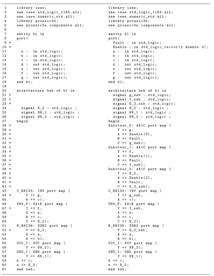
FIGURE 3.4 – Comparison of VHDL files before and after adding the saboteurs. . . 62
FIGURE 3.5 – Example circuit for input patterns extraction. . . 63
FIGURE 3.6 – Graphical visualisation of the example VCD file. . . 63
FIGURE 4.1 – Adopted circuits for the internal logic gates of the Versatile CLB. . 72
FIGURE 4.2 – VersaTile internal structure with the adopted IDs. . . 72
FIGURE 4.3 – VersaTile configured as an AND3 macro. . . 78
FIGURE 4.4 – VersaTile configured as an DFN1C0 macro. . . 78
FIGURE 4.5 – SET susceptibilities of the 2-input combinational functions. . . 83
FIGURE 4.6 – SET susceptibilities of some 3-input flip-flop macros. . . 83
FIGURE 4.7 – SET susceptibilities of some 3-input latch macros. . . 83
FIGURE 4.8 – Percentage of generated SEUs for some 3-input flip-flop macros. . . 83
FIGURE 4.9 – Percentage of generated SEUs for some 3-input latch macros. . . 84
FIGURE 5.1 – Errors of the SEV estimation processes. . . 97
FIGURE 5.2 – Simulation time of the SEV estimation processes. . . 99
FIGURE 6.1 – Proposed emulation-based platform. . . 102
FIGURE 6.2 – Illustration of the serial message reporting a SET injection. . . 105
FIGURE 6.4 – Time vs. place uniform SET distribution for the c8 benchmark. . . 111
FIGURE 6.5 – Time vs. place weighted SET distribution for the c8 benchmark. . . 111
FIGURE 6.6 – Time vs. place uniform SET distribution for the comp benchmark. . 111
FIGURE 6.7 – Time vs. place weighted SET distribution for the comp benchmark. 112 FIGURE 6.8 – Uniform SET distribution for the c8 benchmark. . . 114
FIGURE 6.9 – Weighted SET distribution for the c8 benchmark. . . 114
FIGURE 6.10 –Uniform SET distribution for the comp benchmark. . . 114
FIGURE 6.11 –Weighted SET distribution for the comp benchmark. . . 115
FIGURE 6.12 –Comparison between SEV estimation using logic simulation and em-ulation. . . 117
FIGURE C.1 – SET quantised delay model. . . 151
FIGURE C.2 – SET emulation considering electrical masking effects. . . 151
FIGURE C.3 – Electrical pulse generation circuit. . . 153
FIGURE C.4 – Saboteur Candidates. . . 154
FIGURE C.5 – Transient electrical pulses observed at an output of the FPGA. . . . 156
FIGURE C.6 – Dissociation between pulses and system clock. . . 156
FIGURE C.7 – Comparison between local and global net for pulse distribution. . . . 158
List of Tables
TABLE 3.1 – Intermediate table of the input patterns extraction process. . . 65
TABLE 4.1 – ProASIC3E A3PE1500-PQ208 main features. . . 70
TABLE 4.2 – VersaTile transistors. . . 73
TABLE 5.1 – Combinational benchmark circuits. . . 87
TABLE 5.2 – SEV estimation at the transistor level . . . 90
TABLE 5.3 – SEV estimation adopting uniform distribution . . . 92
TABLE 5.4 – SEV estimation adopting the simplified strategy . . . 94
TABLE 5.5 – SEV estimation adopting the complete strategy . . . 96
TABLE 6.1 – Benchmark circuits used in emulation. . . 107
TABLE 6.2 – Resources consumption of the emulation platform with the cm152a benchmark. . . 108
TABLE 6.3 – Resources consumption of the emulation platform with the cmb benchmark. . . 108
TABLE 6.4 – Resources consumption of the emulation platform with the c8 bench-mark. . . 109
TABLE 6.5 – Resources consumption of the emulation platform with the comp benchmark. . . 109
TABLE 6.6 – Estimated SEV using the emulation platform. . . 116
TABLE A.1 – Configuration vectors for the combinational macros. . . 133
TABLE A.2 – Configuration vectors for the flip-flops. . . 137
TABLE A.3 – Configuration vectors for the latches. . . 139
TABLE B.1 – SET susceptibilities for the combinational macros. . . 140
TABLE B.2 – SET susceptibilities for the flip-flops. . . 144
TABLE B.3 – SEU susceptibilities for the flip-flops. . . 146
TABLE B.4 – SET susceptibilities for the latches. . . 148
TABLE B.5 – SEU susceptibilities for the latches. . . 149
TABLE C.1 – Resulting pulse widths for SET emulation. . . 157
TABLE D.1 – Circuits combinatoire de référence – Caractéristiques et résultats de l’estimation SEV. . . 178
List of Abbreviations and Acronyms
2D Two-Dimensional
3D Three-Dimensional
ALM Adaptive Logic Module
AMUSE Autonomous Multilevel emulation system for Soft Error evaluation ASEE Analogue Single-Event Effects
ASET Analogue Single-Event Transient ASEU Analogue Single-Event Upset
ASIC Application-Specific Integrated Circuit CCC Clock Conditioning Circuits
CCD Charged-Coupled Device CLB Configuration Logic Block CME Coronal Mass Ejection
CMOS Complementary Metal Oxide Semiconductor CSV Comma-Separated Value
DD Displacement Damage
DRAM Dynamic Random-Access Memory DSE Device Single Event
DSET Digital Single-Event Transient DUT Device Under Test
EPP Error Propagation Probability
FERRARI Fault and Error Automatic Real-Time Injection FET Field Effect Transistor
FIFA Fault Injection and Fault masking Analysis FIFO First-In First-Out
FIT Failures In Time
GCR Galactic Cosmic Radiation HDL Hardware Description Language HZE High Z and Energy
IC Integrated Circuit IOC Input and Output Cell LAB Logic Array Block
LC Logic Cell
LED Light-Emitting Diode LEO Low Earth Orbit LET Linear Energy Transfer
LFSR Linear-Feedback Shift Registers LP Latching Probability
LUT LookUp Table
LVTTL Low-Voltage Transistor Transistor Logic MBU Multiple-Bit Upset
MCU Multiple-Cell Upset
MEFISTO Multi-level Error/Fault Injection Simulation Tool MOPITT Measurements Of Pollution In The Troposphere MOS Metal Oxide Semiconductor
MOSFET Metal Oxide Semiconductor Field Effect Transistor MTBF Mean Time Between Failures
NIEL Non-Ionising Energy Loss NLC Non-Linear Counter NMOS N-channel MOSFET
OSVVM Open Source VHDL Verification Methodology OTP One-Time Programmable
PGM Probabilistic Gate Models PGP Pulse Generation Probability PLB Programmable Logic Block PLL Phase-Locked Loop
PMOS P-channel MOSFET
PRNG Pseudo-Random Number Generator PROM Programmable Read-Only Memory PTM Probabilistic Transfer Matrices PVW Probabilistic Vulnerability Window
RAM Random-Access Memory
ROM Read-Only Memory
RTL Register-Transfer Level
SAMA South-Atlantic Magnetic Anomaly
SCFIT Shadow Components-based Fault Injection Technique SCM Stochastic Computational Model
SCR Silicon Controlled Rectifier, Solar Cosmic Radiation
SE Soft-Error
SEB Single-Event Burnout SEE Single-Event Effect
SEFI Single-Event Functional Interrupt SEGR Single-Event Gate Rupture
SEL Single-Event Latch-up SER Soft-Error Rate
SET Single-Event Transient SEU Single-Event Upset SEV Soft-Error Vulnerability SHE Single-Event Hard Error
SoC System on Chip
SP Signal Probability SPE Solar Proton Event
SPICE Simulation Program with Integrated Circuit Emphasis SRAM Static Random-Access Memory
TAP Test Access Port
TCS Triple Constraint Satisfaction TID Total Ionising Dose
TMR Triple Modular Redundancy USB Universal Serial Bus
VCD Value Change Dump
VERIFY VHDL-based Evaluation of Reliability by Injecting Faults Efficiently VFIT VHDL-based Fault Injection Tool
VHDL VHSIC Hardware Description Language VHSIC Very High Speed Integrated Circuits VITAL VHDL Initiative Towards ASIC Libraries
List of Symbols
φ particle flux ϕ particle fluency σ cross-section χ susceptibilidade D absorbed dose E particle energy R SEE rate Z atomic numberContents
1
Introduction
. . . . 171.1 Motivations . . . . 20
1.2 Objectives and Contributions . . . . 21
1.3 Text Organisation . . . . 23
2
Concepts and Literature Review
. . . . 252.1 Radiation Effects on Electronic Devices . . . . 26
2.1.1 Radiation Environment . . . 26
2.1.2 Radiation Interaction with the Matter . . . 29
2.1.3 Classification of the Radiation Effects on the Electronics Devices . . . 31
2.1.4 Soft-Error Rate and Soft-Error Vulnerability . . . 34
2.2 Error-Masking Factors . . . . 36
2.2.1 Logical Masking . . . 37
2.2.2 Electrical Masking . . . 39
2.2.3 Latching-Window Masking . . . 39
2.3 Methods for Soft-Error Analysis . . . . 40
2.3.1 Analytical . . . 41
2.3.3 Logic Simulation . . . 43
2.3.4 Emulation . . . 44
2.3.5 Software Fault-injection . . . 47
2.3.6 Hardware Tests . . . 47
2.3.7 Radiation Tests . . . 48
2.4 SET Susceptibility on SEV Estimation . . . . 49
2.5 CLB Architectures . . . 50
3
Proposed Strategy for SEV Estimation
. . . . 553.1 Simplified Version of the Strategy . . . . 57
3.2 Complete Version of the Strategy . . . . 58
3.3 Adding Saboteurs . . . . 61
3.4 Extraction of the Input Patterns Distribution . . . . 63
3.5 Calculation of the SET Susceptibilities . . . . 66
3.6 Generating the Testbench for SEV Estimation . . . . 67
4
Estimation of the SET Susceptibilities
. . . . 694.1 Analysed Technology . . . . 70
4.2 CLB Simulation Model . . . . 71
4.3 Definition of the Configuration Vectors . . . 76
4.4 CLB Library . . . . 79
4.5 Estimation of the SET Susceptibilities . . . . 80
4.6 Results . . . . 81
5.1 Analysed Benchmarks . . . . 86
5.2 Operational Scenarios . . . 88
5.3 SEV Estimation at the Transistor Level . . . . 88
5.4 SEV Estimation adopting Uniform Distribution . . . . 91
5.5 SEV Estimation adopting the Simplified Strategy . . . . 93
5.6 SEV Estimation adopting the Complete Strategy . . . . 95
5.7 Comparative Analysis . . . 97
6
Using the Proposed Strategy with Emulation
. . . . 1006.1 Use with Host-Based Emulation Approach . . . 101
6.2 Use with Autonomous Emulation Approach . . . 101
6.3 Proposed Emulation-Based Framework . . . 102
6.4 SET Distribution Scheme . . . 105
6.5 Evaluation of the Proposed Emulation Platform . . . 106
6.5.1 Analysed Circuits . . . 107
6.5.2 Resources Consumption . . . 107
6.5.3 SET Distribution Analysis . . . 110
6.5.4 Estimated SEV . . . 115
7
Conclusions and Perspectives
. . . . 1187.1 Main Contributions . . . 119
7.2 Future Work . . . 121
7.3 Publications . . . 123
7.3.1 Conference Proceedings . . . 123
Bibliography
. . . . 124Appendix A – Configurations of the VersaTile Functions
133Appendix B
–
SET Susceptibilities of the VersaTile
Functions
. . . . 140Appendix C – Self-Produced Transients for SET
Emu-lation
. . . . 150 C.1 Context . . . 150 C.2 Evaluation Process . . . 152 C.2.1 Evaluation Environment . . . 152 C.2.2 Analysed Characteristics . . . 154 C.2.3 SET Emulations . . . 155C.3 Evaluation Test Cycles . . . 155
Appendix D – Résumé Français
. . . . 159D.1 Introduction . . . 159
D.2 Concepts et revue de littérature . . . 162
D.3 Stratégie proposée pour l’estimation SEV . . . 168
D.4 Estimation des susceptibilités SET . . . 173
D.5 Évaluation de la stratégie proposée . . . 175
D.6 Utilisation de la stratégie proposée avec émulation . . . 179
1 Introduction
In digital systems, a Soft Error (SE) is a wrong value in a signal or data register that is not permanent, i.e., the system can restore its operational state after the treatment of the SE. Contrarily, a hard error is a permanent effect, usually caused by damage, but can also be a design mistake, for instance.
There are many possible causes for SEs, including voltage scaling, ageing, crosstalk, electromagnetic interference, hazard effects, and radiation. The occurrence of a SE com-monly depends on some device characteristics and external factors, as the environment and the device operation.
For example, the SEs produced due to the voltage scaling depends on the operational temperature of the device. The ageing leads to a permanent change in the device charac-teristics that may result in timing issues for some operational scenarios and environmental conditions, generating SEs. If the error due to the ageing effects occurs independently of the environment and operation, it becomes a hard error.
Similarly, crosstalk depends on the susceptibility of the circuit and the characteristics of the signal that induces the SE between circuit lines. The electromagnetic interference depends on the characteristics of the electromagnetic signal and the circuit susceptibility. The hazard effects are a significant concern on asynchronous circuits, in which they may occur due to the implementation of the circuit and the sequence of the signal changes, likewise the previous cases.
The radiation effects may induce SEs due to the ionisation of the electronic device. Thus, they also depends on the susceptibility of the circuit and the characteristics of the
radiation environment.
Although the adopted definition of a SE covers any cause, in many works the term Soft Error is associated exclusively to the radiation effects. This work also focuses on the SEs caused by radiation. More specifically, the SEs that are directly produced by the Single-Event Effects (SEEs), that is the class of ionising radiation effect generated by a single ionisation particle. Differently, the Total Ionising Dose (TID) is another class of ionising effect that may resemble the ageing effect and could indirectly cause SEs, but is out of the scope of this work.
The first SEE of interest is Single-Event Transient (SET), that is a temporary change in the logic value of a node, caused by an excursion on its voltage. This voltage excursion results from the transient current pulse produced by the recombination of the ions induced by the ionisation particle.
The SET is generated in the sensitive area of the transistors that compose the logic elements and can affect them in different ways. For the combinational elements (logic gates), the SET can propagate to the output or can be filtered out internally. For the sequential elements (registers – latches and flip-flops), the SET can also propagate to the output or be filtered, but these are minor effects. For them, the primary effect is the Single-Event Upset (SEU), that is the change of the stored value, that holds until the next write cycle. Similarly, for the memory cells, the SEU is also the major concern.
The reliability assessment of digital systems adopts the Soft-Error Rate (SER) as the metric associated with the SEs. This parameter is intrinsically related to the rate of transient electrical pulses, R, generated in the transistors of the circuit. However, the circuit’s SER is not the sum, or combination, of the R value of each transistor. The logical, electrical, and latching-window masking effects filter many transient pulses. It is difficult to obtain a mathematical formula for the SER, based on the radiation and circuit characteristics, that also includes these masking effects. This difficulty led to the development of many SER estimation methods.
radia-tion tests approaches, among others. However, except for the radiaradia-tion tests, they do not deal directly with the SER, as it requires the ionising particle flux. Instead, they deal with the probability of occurrence of a SE, adopting terms like SE sensitivity, susceptibility or vulnerability. In this work, we adopt two terms. For the probability of occurrence of SEs at the output of the gate-level components due to the SETs generated in their internal transistors, we use the term SET Susceptibility. For the probability of occurrence of SEs at the output of the circuit, we adopt the term Soft-Error Vulnerability (SEV).
We differentiate these two probabilities because we focus on the influence of the SET susceptibilities when evaluating the SEV at the gate level. This influence is taken into account by some classes of estimation methods (analytical and electrical simulation) but ignored by others (logic simulation and emulation), as briefly introduced below.
In Buard and Anghel (2011), the authors present a logic gate modelling and simulation method at the transistor level using SPICE (Simulation Program with Integrated Circuit Emphasis). Their method intrinsically includes the internal logical masking, with the influence of both the logic gate internal circuitry and the input values (hereafter referred to as input patterns). It also includes the electrical masking, through the electrical modelling of the transistors and the SETs. Their results show that both logical and electrical masking effects affect the SET susceptibility of the analysed logic gate.
The analytical method proposed in Rezaei et al. (2014) also includes the internal masking effects of the logic gates. A major concern of the authors is how the input patterns influence the SET generation at the output of the logic gates. Their results also show that the SET susceptibilities are affected by these factors and, additionally, how they influence the circuit SEV.
In opposition, the logic-simulation methods presented in Jenn et al. (1994), Baraza et
al. (2005), and Lopes Filho and D’Amore (2012), and the emulation methods presented
in Civera et al. (2001), Entrena et al. (2012), and Ebrahimi et al. (2014) do not take the SET susceptibilities into account. Unlike the previously mentioned methods, these do not deal with transistors. They work directly at the Register Transfer Level (RTL) for
logic simulation, or gate-level for emulation, on the output of its components. As they inject the SEs uniformly, they intrinsically assume that all components have the same SET susceptibility.
In this context, we propose a SEV estimation strategy that takes into account the SET susceptibilities of the logic elements of the circuit. This approach is intended for use with a logic-simulation approach, but may be adapted for use with emulation platforms. The SET injection process follows a weighted distribution, for which the weights are the SET susceptibilities of the logic elements.
Since this probability-aware approach requires accessing the output of the logic ele-ments, the simulation requires the use of the post-synthesis back-annotated file, that is a netlist with the logic elements for the target technology. This approach can be ap-plied to both Application-Specific Integrated Circuits (ASICs) and Field Programmable Gate Arrays (FPGAs). However, in this work, we targeted only a specific FPGA family. For this reason, hereafter, we usually refer to the logic elements directly as the CLBs (Configuration Logic Blocks) of an FPGA.
The adoption of the proposed SEV estimation method requires the SET susceptibilities for the target technology. As this information is not available, we estimated the SET susceptibilities of the CLBs of the selected technology.
To evaluate the proposed approach, we estimated the SEV for a set of benchmark circuits. Finally, we explore the adoption of the proposed strategy with an emulation platform.
1.1
Motivations
The SER is an essential reliability metric to evaluate how the electronics systems behave in the radiation environment. Its estimation is part of the radiation analysis and is useful for supporting design decisions that can affect since the adopted technology to the architectural solution. For this reason, the SER estimation needs to be obtained as
soon as possible in the design cycle.
In critical applications, as some aerospace projects and nuclear plants, it is common to adopt conservative approaches, in which they only use radiation-hardened or tolerant devices. These devices will not produce or produce very few SEs due to the nominal expected radiation. In these cases, a conservative approach for the SER estimation may be enough for the radiation analysis, approving or rejecting the use of the device or design solution.
However, depending on the application, a higher SER may be acceptable, although it is always desirable to minimise it, pursuing an optimal solution. In these cases, a more accurate SER estimation approach would be more suitable than a conservative one, since it enables the comparison between possible solutions. It is especially attractive for FPGAs, in which it is possible to have many alternative solutions using the same device technology.
This scenario motivated us to propose a strategy that improves the SEV and conse-quently the SER estimation accuracy, while it applies early on the design cycle since it is applicable as soon as there are a circuit netlist and a desired operational scenario, without requiring the real device.
1.2
Objectives and Contributions
The main objective of this work is to incorporate the specific SET susceptibility of each logic gate of a given device into the SEV estimation approaches based on, primarily, logic-simulation, and emulation. With this purpose, this work introduces a probability-aware fault-injection strategy that distributes the SETs into the circuit nodes, at the gate level, following a weighted distribution defined by the SET susceptibilities. The proposed strategy aims the following features:
• be flexible, not restricted to any HDL language, logic-simulator, or synthesiser; • be of general use, not limited to any circuit architecture;
• can be easily incorporated to the verification flow; • can be automated by scripts.
In fact, this work brings two versions of this strategy. A simplified version assumes that the SET susceptibilities depends only on the logic gate internal circuitry, while a complete version additionally takes into account how the circuit operation affects the SET susceptibility of each logic gate. The first one requires less information and data processing, and is less accurate, while the second is more accurate, but requires more information and data processing.
The strategy relies on the SET susceptibilities of the logic gates. However, this infor-mation is not usually available. For this reason, this work includes the estiinfor-mation of the SET susceptibilities of the CLBs of a target FPGA family, that was used to evaluate the proposed strategy.
The strategy for SEV estimation and the adopted process for SET susceptibility esti-mation focus on the logical masking effect, due to the logic gate circuitry and the input patterns generated by the circuit operation. The electrical and the latching-window mask-ing effects are out of the scope of the work, primarily, due to the lack of electrical and timing details from the selected technology, but also because they are not directly related to the input pattern effects.
The application of the proposed strategy concentrate on the logic-simulation approach, adopted for the evaluation of the strategy. However, the work includes a discussion about the adoption of the strategy with emulation approaches, emphasising on the SET distribution mechanism.
In summary, the main contributions of this work are the probability-aware fault-injection strategy, the reference SET susceptibilities for the analysed technology, and the probabilistic fault-distribution approach for use in emulation platforms.
1.3
Text Organisation
Chapter 1, Introduction, contextualise the work and presents its motivations, objec-tives, a summary of contributions and the organisation of the text.
Chapter 2, Concepts and Literature Review, brings the concepts used in this work along with the bibliographic review that supports the proposed strategy. This chapter describes the effects of the ionising radiation on the electronics devices, that are the source of the SEs analysed in this work, and the error-masking factors that influence the SEV. Additionally, this chapter presents the various methods for SE analysis and briefly describes the examples found in the literature.
Chapter 3, Proposed Strategy for SEV Estimation, details our probability-aware strat-egy for the estimation of the SEV of a digital circuit based on the SET susceptibilities of its logic gates. We propose two alternatives for this strategy, a simplified and a complete one. The simplified requires less information and data processing, but results in a lesser accurate estimation, while the complete needs more information and data processing, but is more accurate. This chapter presents the estimation process for both alternatives, de-scribing each step of these processes. The simplified strategy is based on a preliminary study presented in Armelin et al. (2016), while the complete one is based on Armelin et
al. (2019).
Chapter 4, Estimation of the SET Susceptibilities, describes how we estimated the SET susceptibilities used in this work. First, this chapter presents and briefly compares various architectures of CLBs from the most commonly used FPGA families. Then, it details the architecture of the CLB that was selected for this work. Finally, it details the CLB modelling at the transistor level, its configuration to the various functions, and the estimation process to obtain the reference SET susceptibilities.
Chapter 5, Evaluation of the Proposed Strategy, presents how we evaluated the pro-posed strategy, described in Chapter 3, using a simulation-based environment. This chap-ter presents the analysed circuits, and the four distinct SEV estimation processes used in the analysis. The first estimation considers the CLB model at the transistor level,
detailed in Chapter 4, to obtain a basis of comparison for the others estimations. The second one resembles the approaches found in the literature, that consider the same SET susceptibility for all logic gates. The third and fourth estimations respectively adopt the simplified and completed proposed strategies described in Chapter 3. Finally, by the end of the chapter, we present the results, regarding the estimated SEV and the simulation time.
Chapter 6, Using the Proposed Strategy with Emulation, brings some considerations regarding the use of the proposed strategy with an emulation-based environment. We took into account the variations of emulation-based approaches presented in Chapter 2. Additionally, this chapter details the implementation of an emulation-based environment that uses the proposed strategy, focusing on its ability to distribute the SETs according to the susceptibility of each logic gate. The last part of this chapter is based on Armelin
et al. (2018a).
Chapter 7, Conclusions and Perspectives, discuss the conclusions of this work and some perspectives of future works.
Appendix A, Configurations of the VersaTile Functions, reports the details of the configuration of the analysed CLB model for each implemented function.
Appendix B, SET Susceptibilities of the VersaTile Functions, lists the SET suscepti-bility of each function implemented with the analysed CLB model.
Appendix C, Self-Produced Transients for SET Emulation, describes an strategy for SET emulation, that were used with the emulation-based environment presented in Chap-ter 6. This Appendix is based on Armelin et al. (2018b).
2 Concepts and Literature Review
The proposed strategy for SEV estimation of digital circuits taking into account the SET susceptibilities of their logic gates is an incremental contribution to the scientific community efforts to properly analyse and predict the behaviour of electronic devices on a radiation environment.
In this chapter, we present the concepts and the literature review concerning the main topics of interest for this work. In Section 2.1, we introduce the effects of the radiation on the electronics devices, covering the radiation environment, the interaction of the radiation with the matter, and the classification of the radiation effects on electronics devices, characterising the SEs analysed in this work. This section also presents a discussion about the correlation between the terms Soft-Error Rate and Soft-Error Vulnerability.
In Section 2.2, we discuss the error masking factors that are intrinsically correlated to the Soft-Error Rate of digital circuits, i.e., the logical, the electrical, and the latching-window masking.
Section 2.3 presents seven classes of methods used for analysing the effects of the SEs on digital systems. This section covers the radiation tests, the analytical methods, the electrical and logic simulations, and the emulation-based methods. For each method, we present some examples found in the literature.
In Section 2.4, we present our analysis on how the SET susceptibility of the logic gates are taken into account by the various methods and examples described in the previous section. This analysis led to the strategy for SEV estimation proposed in this work, that we applied for an specific FPGA technology.
Finally, in Section 2.5, we present some CLB architectures from the most known manufacturers, covering since the first devices to some of the most advanced ones.
2.1
Radiation Effects on Electronic Devices
The effects of the radiation on electronics devices is a complex knowledge field that comprises the sources of the radiation, how they interact with the semiconductors and the effects of this interaction on the behaviour of these devices.
For this work, the main interest is on the later part, more specifically on how the transient electrical pulses generated in the basic semiconductor elements affect the outputs of a digital circuit. For this reason, this section presents a brief introduction to the radiation environment and their interaction with the matter, followed by a more detailed classification and description of the effects of the radiation on the electronic devices.
A detailed description of the radiation environment and their effects on electronics devices may be found in Holmes-Siedle and Adams (2002), Claeys and Simoen (2002), Okuno and Yoshimura (2010), and Velazco et al. (2007).
2.1.1
Radiation Environment
The radiation environment is a heterogeneous mixture of many types of radiations, with a wide range of energy (E) and flux, coming from different sources. For this reason, each intended application, e.g., space, aeronautics, ground-level operation, and radioactive installation, has a specific associated radiation environment.
As discussed in Pereira Junior (2015), the radiation can be divided into five types: electromagnetic (photons – x-rays and gamma-rays); light charged particles (electrons and positrons); heavy charged particles (protons, alpha particles, fission fragments, and other ions); neutral particles (neutrons); and elementary particles (resulting from the interaction of the cosmic radiation with the atmosphere).
Concerning the near-Earth space-environment, there is two sources of radiation: the Galactic Cosmic Radiation (GCR) that comes from outside the Solar System, and the Solar Cosmic Radiation (SCR), coming from the Sun activities.
The GCR is composed of high-energy particles that were probably generated by high energetic phenomena, e.g., pulsars and supernova explosions. It is mainly composed by protons (hydrogen nuclei) and alpha particles, but it also has heavier nuclei (HZE-particles – High atomic number, Z, and Energy) and electrons (REITZ, 2008).
The SCR comprise two components: the nearly continuous solar wind, that is the continuous solar activity that emits low-energy protons and electrons; and a periodic one, in which the Sun releases particles with higher energy in events like Solar Proton Event (SPE), Coronal Mass Ejection (CME), and Solar Flares during the approximately seven years of high activity of its nearly eleven years period (BOUDENOT, 2007;REITZ, 2008).
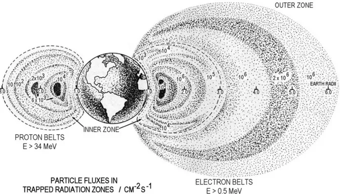
These cosmic radiations interact with the Earth magnetic field, which may trap the particles, deflect them or let them pass through. The trapped particles form the Van Allen Radiation Belts, illustrated in Fig. 2.1.
FIGURE 2.1 – Trapped Radiation – The Van Allen Belts. On the left, a representation of the proton flux inside the inner belt. On the right, a representation of the electron flux inside both inner and outer belts. Source: reproduced from Reitz (2008).
These radiation belts consist of electrons, protons, and some heavier ions (REITZ,
2008). Although this trapped radiation results from the interaction of the cosmic radiation with the Earth magnetic field, it is also considered as a radiation source, due to its relevance to the aerospace applications.
The Earth magnetic field presents some anomalies, as the South-Atlantic Magnetic Anomaly (SAMA), that interfere in the local radiation environment. The SAMA is a region where the magnetic field is weaker than in other regions at similar altitude and latitude. This anomaly leads the inner radiation belt to come closest to the surface of Earth, increasing the radiation flux at lower altitudes. Fig. 2.2 illustrates how the SAMA may affect Low Earth Orbit (LEO) satellites, showing the reported events for the MOPITT (Measurements Of Pollution In The Troposphere) mission, concentrated in the SAMA region.
FIGURE 2.2 – MOPITT Device Single Events (DSEs). Geographical distribution of the DSE reported by the Measurements Of Pollution In The Troposphere mission. The SAMA can be identified by the density stop. Source: reproduced from Nichitiu et al. (2004).
The cosmic radiation may also interact with the dense matter present in the Earth atmosphere, in a nuclear spallation process, in which the cosmic radiation transfer its energy through elastic and inelastic collisions with the nuclei. This interaction produces a
radiation shower that includes neutrons and elementary particles. Due to this interaction, a small part of the cosmic radiation reaches the Earth surface (both the Earth magnetic field and atmosphere act like radiation shields). Additionally, the resulting atmospheric radiation environment depends on the altitude of interest.
The energy of the GCR particles ranges to above 10 GeV per nucleon (
STASSINOPOU-LOS; RAYMOND, 1988). For the SCR, the solar wind has low-energy particles, in the range
from 0.5 to 2 keV per nucleon, while the SPE, CME, and solar flares have high-energy particles, from tens of MeV to hundreds of GeV per nucleon (BOUDENOT, 2007).
In the radiation belts, the electrons may have energy up to 5 MeV in the inner belt and may reach 7 MeV in the outer belt, while the protons of the inner belt may reach tens of MeV. When a high-energy solar event occurs, the energy of the electrons may reach tens of MeV, while the energy of the protons may reach hundreds of MeV (BOUDENOT,
2007).
Finally, as reported by Federico et al. (2010), the energy of neutrons induced by cosmic radiation may reach tens of MeV.
2.1.2
Radiation Interaction with the Matter
The interaction of the radiation with the matter can be divided into two classes, according to the characteristics of the radiation: charged and uncharged particles. The charged particles, also known as directly ionising particles, are subdivided into heavy and light particles. The uncharged particles, also known as indirectly ionising particles, are subdivided into electromagnetic (photons – considered as particles with energy and momentum) and neutrons. Based on Okuno and Yoshimura (2010) and on Pereira Junior (2015), in this section we list the different interaction mechanisms for each radiation and the main physical quantities involved.
The charged particles usually interact with the atomic electron cloud, but they may interact with the whole atom or its nucleus. The possible interactions are the soft collision (inelastic atomic collision), hard collision (inelastic collision with electrons of inner shells),
elastic and inelastic collision with the nucleus, nuclear reaction, and positron annihilation. For the heavy particle, the ionisation along its trajectory is denser than those produced by light particles, and the stopping distance of heavy particle is shorter than those of the light ones. The trajectory of the heavy particle is nearly rectilinear, while the trajectory of the light particles may present large deflections from the original direction. The energy transferred to the matter depends on the distance the particle travels in it. The Linear Energy Transfer (LET) is the physical quantity used to express how much energy a particle deposits by each travelled distance unit. It is usually expressed in MeV/cm, but may also be expressed in terms of MeV.cm2/mg. Lastly, besides the ionisation, the charged particles
may also lead to atomic displacement.
The photons may ionise the matter through the photoelectric effect, the Compton effect and the pair production. The interactions of the photons with the matter also produce a cascade of secondary radiation, with photons, electrons and positrons that leads to further ionisation. The LET is smaller than those from the charged particles.
Finally, the free neutrons primarily interact with the nuclei of the atoms because there is no Coulomb interaction with the charged elements. Moreover, since there is no Coulomb repulsion, even low energy neutrons may interact with the nuclei. The possible interactions are the elastic and inelastic scattering, and the absorption nuclear reactions that produce secondary radiations (as beta- and gamma-radiation) that may ionise the matter. Thus, the effects of the neutron radiation are the atomic displacement and the ionisation of the matter.
Besides the LET, there are some other physical quantities related to the radiation. The Absorbed Dose, D, is the amount of transferred energy per unit mass, expressed in gray, Gy = J/kg, or rad = 0.01 Gy. The cross-section, σ, is the area transverse to the relative motion between the particle flow and the target matter, expressed in cm2. The
particle flux, φ, is the rate of particle flow per unit area, expressed in [counts]/cm2.s, while
the particle fluency, ϕ, is the particle flow per unit area, or the integrated flux in time, expressed in [counts]/cm2.
2.1.3
Classification of the Radiation Effects on the Electronics
Devices
There are three classes of radiation effects on the electronics devices: the Displacement Damage (DD), the Total Ionising Dose (TID), and the Single-Event Effect (SEE). The DD and TID are cumulative effects, meaning the effects will be perceptible only after the interaction of many radiation particles with the matter, while the SEE is a singular effect, caused by the interaction of a single radiation particle.
The DD is a non-ionising cumulative effect caused by the charged particles and neu-trons that interact with the nuclei of the atoms. This effect affects the structure of the material and leads to long-term degradation in optoelectronics, e.g., increasing the dark current of Charged-Coupled Devices (CCDs), as discussed by Srour et al. (2003), and altering the response of Silicon Carbide (SiC) Light-Emitting Diodes (LEDs), as reported by Hinrichsen et al. (1998). The Non-Ionising Energy Loss (NIEL) is the physical quan-tity associated with the particles that may produce DD, expressed in MeV.cm2/g. Lastly,
Srour et al. (2003) present a review of the DD effects in silicon devices.
The TID is a cumulative ionising effect induced by any interaction of radiation par-ticles with the matter that leaves trapped charges in the device structure, i.e., ionising interactions that are not fully recombined. These charges trapped inside the semiconduc-tor, or the oxide, change the device characteristics, as the voltage threshold and leakage current of a MOSFET transistor (FACCIO; CERVELLI, 2005). There are many studies
de-voted to the TID effects on electronics devices. Barnaby (2006) discusses the TID effects on modern CMOS technologies, while Ding et al. (2015) report the TID effects in 65 nm CMOS transistors. Snow et al. (1967) reported one of the first studies about the charges accumulation on the isolation oxide, and Armani et al. (2015) compare the TID response of some FPGAs and memories.
The SEE is an effect induced by a single radiation particle with enough LET to provoke a relevant disturbance in the device behaviour. The SEE is the class of radiation effects of interest in this work, which is the reason why it is discussed in more details in the
remainder of this section.
The primary SEE is the Single-Event Transient, that is a voltage excursion in a circuit node inside the device. When the ionising radiation strikes through a reverse-biased junction, the electric field induces a transient current with the produced free charges. This transient current causes a momentary voltage excursion in the electric node. Fig. 2.3 illustrates a SET modelling for a CMOS inverter.
FIGURE 2.3 – SET modelling for a CMOS inverter. The figure illustrates two situations: a particle strike in the PMOS and in the NMOS. In both cases, it will induce a transient current between the struck area and the body. Source: adapted from Buard and Anghel (2011).
The SET effects on analogue devices are different from digital ones. For this reason, some works use specific acronyms to differentiate them: Digital Single-Event Transient (DSET), for digital circuits, and Analogue Single-Event Transient (ASET) for analogue and mixed-signal circuits. Further, some older works related to SEE in analogue circuit adopted the more generic term ASEE (Analogue Single-Event Effects) to refer to the transients, as in Turflinger (1996), or even the term ASEU (Analogue Single-Event Upset), as in Koga et al. (1993), that would be the analogue version of the Single-Event Upset (SEU).
The first reports of SEUs were published by Binder et al. (1975) and Pickel and Blandford (1978), while the first studies on DSET were published by Diehl et al. (1983). Regardless, the nature of the DSETs and ASETs are the same. The main difference is that the analogue circuits are susceptible to any voltage disturbance, while the digital circuits are susceptible to voltage disturbances that exceed the logic threshold. In this
work, we only deal with digital circuits and adopt the term SET. Finally, Ferlet-Cavrois
et al. (2013) present an extensive review of SETs on digital CMOS.
Another SEE of interest for this work is the already mentioned SEU, which is a change in the stored logic value of a memory element (memory cell, flip-flop, or latch). This effect is also referred to as a bit-flip and sometimes used as a synonymous for Soft-Error. The SEU is produced by the same mechanism that produces the SET when the struck reverse-biased junction is part of a storage element. Fig. 2.4 illustrates the waveform of a storage element signal in two situations: when the voltage excursion results in an SEU and when it does not.
FIGURE 2.4 – Illustration of a SEU. This figure shows the voltage excursion of the storage signals, in a memory element, in two situations: a SEU is produced and no SEU is produced. Source: reproduced from Gaillard (2011).
Depending on the feature size of the adopted technology and the LET of the incident radiation, the resulting SEE may affect more than one circuit node. The Multiple-Cell Upset (MCU) is the occurrence of bit-flips in more than one storage element due to the interaction of a single particle. The Multiple-Bit Upset (MBU) is a particular case of MCU in which the multiple bit-flips occur in the same data word.
However, the SEEs are not restricted to bit-flips and voltage transients. If the ionisa-tion particle hits the parasitic bipolar transistors of a CMOS inverter, acting as a trigger of a Silicon Controlled Rectifier (SCR), it may produce a Single-Event Latch-up (SEL), that is characterised by an induced short-circuit between the power lines. It is potentially
destructive, but can be mitigated by protecting the power lines. Another SEE related to induced high current is the Single-Event Burnout (SEB). Differently from the SEL, the SEB is caused by a localised high current that damages the device.
The SEEs are divided into Soft and Hard Errors. The SEs are the recoverable errors on signals or data registers, while the Hard Error is an irreversible change in the device’s operation. The Hard Error is associated with permanent damage or degradation of the device, and sometimes is referred to as Single-Event Hard Error (SHE), to differentiate from damages and degradations not related to SEE. Among the mentioned SEEs, the SEB is the only SHE, while the SET, SEU, MCU, MBU and SEL are SEs (SLAYMAN,
2011).
There are some other SEEs, e.g., SEFI (Single-Event Functional Interrupt) and SEGR (Single-Event Gate Rupture), to describe specific effects caused by single radiation par-ticles. However, since this work focuses on the SEs observed at the gate-level, i.e., SETs and SEUs, we will not further discuss the other SEEs.
2.1.4
Soft-Error Rate and Soft-Error Vulnerability
The SER is an essential parameter to properly assess the reliability of electronic sys-tems that operate under the effects of the radiation particles. It is usually expressed in FIT (Failures In Time – [counts]/109h), but also in terms of MTBF (Mean Time Between
Failures, in hours). This parameter is intrinsically related to the rate of transient electrical pulses, R, generated in the sensitive internal elements of the device (SLAYMAN, 2011),
R =
Z ∞
0
φ(E) · σ(E) · dE, (2.1)
where φ(E) is the particle flux, σ(E) is the element cross-section, and E is the particle energy.
In digital systems, these sensitive elements are the switching transistors, for which the cross-section is directly related to their drain areas.
However, the device’s SER is not the sum, or combination, of the R value of each transistor. The logical, temporal and electrical masking effects, that are described in the next section, filter-out many transient pulses.
Rewriting (2.1), at the transistor level, the rate of transient electrical pulses, Rq, that
are induced in a transistor by the ionising radiation particles is a function of the particle flux, φ(E), the cross-section of the transistor, σq(E), and the particle energy, E, as shown
in (2.2). In other words, the only parameter that is related to the device is σq(E).
Rq=
Z ∞
0
φ(E) · σq(E) · dE (2.2)
At the gate level, the rate of induced pulses inside the logic gate, Ri, depends on the
new sensitive cross-section, σc(E), that is the sum of the σq(E) of each of its transistors,
shown in (2.3). For a circuit with n transistors with the same σq(E), Ri can be obtained
with (2.4). Ri = Z ∞ 0 φ(E) · σc(E) · dE (2.3) Ri = n · Z ∞ 0 φ(E) · σq(E) · dE (2.4)
However, the generated SEs at the logic gate output, Ro, additionally depends on its
internal circuit and operation, being subjected to electrical, logical and temporal masking effects (see Section 2.2). At this level, Ro can be correlated to Ri through a susceptibility
factor, χgate, as in (2.5).
Ro = χgate· Ri (2.5)
Similarly, at the Register-Transfer Level (RTL), the same masking effects may filter-out the the SEs generated at the filter-output of the circuit gates (Rgates), affecting the SER of
shown in (2.6).
SERRT L = χRT L · Rgates (2.6)
Additionally, the SER, at the RTL level, can be correlated to the SEs generated at the transistor level by a parameter that, in this work, we referred to as SEV, as in (2.7).
SERRT L = SEV · Ri (2.7)
As introduced in Chapter 1, in this work we use the term SET susceptibility (χgate)
for the sensitivity of the logic gates to the SEs generated in their transistors, while we use SEV for the sensitivity of the circuits (RTL) to the SEs generated in their transistors.
Depending on the circuit (and logic gate) architecture and operation, SEV (and χgate)
may be a function of the operational clock frequency, the inputs patterns, and the induced transient pulse width. In the next section we describe the masking factors that affect them.
2.2
Error-Masking Factors
The error-masking factors filter-out some of the SEs generated inside of an electronic device. Three types of error-masking factors are relevant for digital circuits: the logical masking, the electrical masking, and the latching-window masking. Each of them has different mechanisms by which the SE may be filtered.
The effects of these masking factors may appear in different hierarchical levels. For this reason, before describing these factors, we present the hierarchical levels considered in this work, and the representation domain associated with them, adapted from Anghel
et al. (2007). The hierarchical levels are:
System Level an item composed by functional blocks, as processors, memory blocks,
Register Transfer Level a functional block composed by logic gates, registers, memory
cells, etc.
Gate Level the logic gates, registers, memory cells, etc., composed by electronic
com-ponents, as transisotrs.
Transistor Level electronic components.
Concerning the representation domain, we may have:
Behavioral functional descriptions define the operation of the device, usually based on
Hardware Description Language (HDL) codes.
Structural components and interconnections describe the device circuit.
Physical equations describe the operation, or the real interaction in the physical device.
2.2.1
Logical Masking
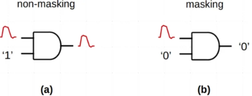
A SE may be logically masked in combinational circuits when one of the inputs has a value that imposes the output value, regardless of the value of the other inputs. Fig. 2.5 illustrates this masking factor. When a 2-input AND gate has one of its inputs receiving logical value ‘1’, a SE on the other input can propagate to the output, in a non-masking situation. However, if one of the inputs of this logic gate receives logical value ‘0’, a SE on the other input is filtered-out, because the output value will be ‘0’, regardless of the value of this second input.
FIGURE 2.5 – Logical masking factor on a 2-input AND gate – (a) non-masking situation and (b) masking situation.
The logical masking is usually taken into account at the RTL and gate levels and its analysis can be extended to the system level. However, when analysing the SE generation inside the logic gate, it is essential to evaluate its masking effect at the transistor level. Fig. 2.6 illustrates the internal masking effect for a 2-input NAND gate.
FIGURE 2.6 – Logical masking factor at the transistor level on a 2-input NAND gate. Each row has one input pattern AB = {00, 01, 10, 11}, while each column has one target transistor {Q1, Q2, Q3, Q4}. For the first input pattern, AB = ‘00’, the output Y changes from ‘1’ to ‘0’ only when the SET occurs in the transistor Q3 (its drain area). For AB = ‘01’, the output Y changes from ‘1’ to ‘0’ only when the SET occurs in the transistor Q3. For AB = ‘10’, the output Y changes from ‘1’ to ‘0’ when the SET occurs in the transistor Q3 or Q4. Finally, for AB = ‘11’, the output Y changes from ‘0’ to ‘1’ when the SET occurs in the transistor Q1 or Q2. This analysis ignores possible layout effects. Assuming all transistors have the same cross-section, χ10 = χ11 = 2 · χ00= 2 · χ01.
This masking factor is usually analysed in the behavioral and structural domain. How-ever, depending on the analysis performed in the physical domain, it can be intrinsically included, as in Buard and Anghel (2011).
2.2.2
Electrical Masking
The electrical masking effect is the successive attenuation of the transient pulse until it is completely quenched. It is caused by the electrical interaction of the transient pulse with the electronic components. Its occurrence depends on the characteristics of the device, as its parasitic capacitances, and of the transient, as its amplitude and width. Fig. 2.7 illustrates this masking factor.
FIGURE 2.7 – Electrical masking factor on two successive inverters – (a) non-masking situation and (b) masking situation.
This masking factor is analysed in the physical domain, at the transistor and gate levels. Nevertheless, its effects may be emulated at the RTL level, in the behavioral domain, as in García-Valderas et al. (2009) and Entrena et al. (2009).
2.2.3
Latching-Window Masking
The latching-window masking effect, or temporal masking effect, is the ‘loss’ of the transient pulse due to its occurrence out of the latching window of the flip-flops and latches. The masking probability depends on the operational frequency of the latching
element and the width of the transient pulse. Fig. 2.8 illustrates this masking factor, that is analysed in the behavioral and structural domain, at the gate, RTL and system levels.
FIGURE 2.8 – Latching-window masking factor on a D flip-flop – (a) non-masking situ-ation and (b) masking situsitu-ation.
2.3
Methods for Soft-Error Analysis
The methods for SE analysis are based on many different techniques, from mathemat-ical models to physmathemat-ical tests. In this section, we describe the most common techniques related to SEV estimation, divided into seven categories: analytical, electrical simulation, logic simulation, emulation, software fault-injection, hardware tests, and radiation tests. As the studies about SET propagation is closely related to the SEV estimation ones, and they may also be divided into some of these categories, we include examples of these stud-ies along with the examples about SEV estimation. Additionally, some of the presented examples deal with both SEs and hard-errors.
The literature has some reviews covering the SE analysis, specially the works related to the fault-injection techniques. Ziade et al. (2004) present a survey of fault-injection tech-niques, divided into hardware, software, simulation, emulation and hybrid-based methods. Although it is outdated, they briefly describe the main techniques available at that time, and compare the advantages and disadvantages of each of this five classes. Kooli and Di-Natale (2014) focused their survey on the simulation-based fault-injection techniques, including the tools that emerged in the decade that separate this review from the
previ-ously mentioned. Jeong et al. (2016) partially updated the survey from Ziade et al. (2004), as they also cover hardware, software, simulation, and emulation-based techniques. How-ever, they focused on those methods suitable for Systems on Chip (SoC). Finally, Natella
et al. (2016) presents a detailed review of software-based fault-injection techniques,
cov-ering software bugs and hardware faults.
2.3.1
Analytical
The analytical methods use some mathematical model to predict the occurrence of SE. These models differ from the semiconductor modelling used in the electrical simulations. They usually deal with the associated probabilities, as the Pulse Generation Probabil-ity (PGP), Error Propagation ProbabilProbabil-ity (EPP), Latching ProbabilProbabil-ity (LP), Probabilis-tic Vulnerability Window (PVW), Transfer Matrices (PTM), ProbabilisProbabilis-tic Gate Models (PGM), and Signal Probability (SP). These methods work at the system, the RTL, and, in most cases, the gate level, with the device representation in the structural domain.
Fazeli et al. (2010) propose an analytical method based on the EPP, from the error generation site to the primary output. The used EPP was derived from another ana-lytical method for SER estimation, proposed in Asadi and Tahoori (2005). Raji et al. (2015) propose a metric, Triple Constraint Satisfaction (TCS), based on PVW, that is an inference of the necessary conditions for the occurrence of a SE. In Rezaei et al. (2014), the authors present a method for SER estimation and mitigation by characterising the input patterns. They analyse the effects of the input patterns on the PGP, while they also use the EPP and LP to obtain the SER. The effects of the input patterns on the SER were also analysed by Sootkaneung and Saluja (2010), that proposed a input reordering technique to reduce the SER, in a work that also adopts electrical simulations to obtain the probabilities.
The influence of the input values on the reliability of digital circuits is taken into ac-count in other analytical based studies, concerning both SEs and hard-errors. In Franco
describe a reliability evaluation method with PGMs, that also deals with signal proba-bilities. While in Han et al. (2014), the authors introduce a stochastic computational approach that uses Stochastic Computational Models (SCMs) and signal probabilities embedded in pseudo-random binary streams.
Finally, Dabiri et al. (2008) proposed an analytical method for power optimisation using gate-sizing that takes the SE impact into account.
2.3.2
Electrical Simulation
The electrical simulation methods are divided into those dedicated to analysing the in-teraction of the radiation particle with the electronic device, based on Three-Dimensional (3D) simulations, and those dedicated to analysing the electrical behaviour of the elec-tronic device, based on circuit simulations similar to SPICE. These methods works at the transistor and gate levels, in the physical domain.
In Dodd (1996), the author discusses the device simulation of charge colection and SEUs, including the drawbacks of adopting Two-Dimensional (2D) and Quasi-3D mod-els instead of 3D ones. Dodd and Massengill (2003) describe the physical mechanisms and 3D modelling of generating SEUs in Dynamic Random-Access Memories (DRAMs) and SRAM Static Random-Access Memories (SRAMs). Dodd et al. (2004) discuss the production and propagation of SETs in logic devices using 3D and circuit simulations, respectively. Similarly, Wirth et al. (2008) adopt SPICE simulation to analyse the SET pulse broadening due to load and propagation effects.
In a different application, Sajjade et al. (2018) use circuit simulation to compare various latches that were radiation hardened by design. This work also present a review of radiation hardened by design techniques.
Finally, as already discussed in the previous section, Sootkaneung and Saluja (2010) use SPICE simulation to obtain the SE probabilities that take into account the input pattern effects. Similarly, Buard and Anghel (2011) showed the influence of the input patterns on the SER of logic gates.
2.3.3
Logic Simulation
The logic simulation methods use HDL models and logic simulator, and can be divided, as discussed in Baraza et al. (2005), into two main groups: those based on simulator commands, and those based on code modification. Additionally, they include a minor generic group for other techniques. Both groups can work on behavioral and structural domains, in system, RTL or gate level.
The methods based on the simulator commands relies on the ability of the chosen logic simulator to modify the values of the signals and timing characteristics of the model during the simulation.
On the other hand, the methods based on the code modification relies on inserting
saboteurs (components that intercept a signal and changes its value) or replacing a
com-ponent by a mutant (a faulty version of the comcom-ponent).
Concerning the code modification methods, mutants are adopted in the studies of both SEs and hard-errors. In Ward and Armstrong (1990) and Ghosh and Chakraborty (1991), the authors use mutants for modelling hard-errors, as stuck-at, in which one or more signals get stuck-at some value, while in Leveugle and Hadjiat (2000), the authors use mutants for modelling SEUs, and that are suitable for use in emulation platforms. The saboteurs are commonly used for SE, as presented in Amendola et al. (1996) and Boue
et al. (1998). For instance, in Lopes Filho and D’Amore (2012), the authors proposed
a fault-injection technique that uses saboteurs to inject SETs and SEUs into a RTL description.
There are some logic-simulation tools for SE analysis, as: MEFISTO (Multi-level Er-ror/Fault Injection Simulation Tool), proposed by Jenn et al. (1994), and the VFIT (VHDL-based Fault Injection Tool), proposed by Baraza et al. (2002), make use of both simulator commands and code modifications; MEFISTO-L, proposed by Boue et
al. (1998), derives from MEFISTO, focusing on the use of mutants; MEFISTO-C,
de-scribed by Folkesson et al. (1998), also derives from MEFISTO, but focus on commands of a specific simulator; and VERIFY (VHDL-based Evaluation of Reliability by Injecting
Faults Efficiently), proposed by Sieh et al. (1997), relies on extending the VHDL language, that fits into the other techniques group.
As examples of logic-simulation fault-injection method at the structural domain, Bot-toni et al. (2015) present a partial triplication approach, in which they use logic-simulation to inject faults into the circuit netlist, for selecting the flip-flops to apply Triple Modular Redundancy (TMR). Similarly, Srinivasan et al. (2005) presented a selective hardening technique for combinational circuits based on netlist logic simulation.
Concerning the studies of SET propagation on combinational circuits, Violante (2003) presents a zero-delay logic-simulation approach that uses circuit expansion to embed tim-ing information, reductim-ing the simulation time.
Finally, a disadvantage of the logic-simulation method is the amount of demanded computational resources. Some works, as Parrotta et al. (2000) and Berrojo et al. (2002), present optimisation techniques for reducing the required simulation time during fault-injection campaigns.
2.3.4
Emulation
The emulation methods for SE analysis are those in which a hardware platform, usually an FPGA, is used to implement the desired circuit functionality, adding some resources to inject faults, or errors, and to detect the propagated errors. They work in the physical domain, at the system, RTL, or gate level.
These methods can be classified according to some characteristics of the whole solution, from which we highlight the four topics described below:
host-based vs. autonomous: In the host-based architectures, the fault-injection and,
in some cases, the error detection are controlled by an external host computer, while in the autonomous ones, these tasks are performed inside the emulation platform, and an external computer is used for data configuration and analysis. The host-based emulation approaches have the advantage of more flexibility to control the