HAL Id: tel-01531870
https://pastel.archives-ouvertes.fr/tel-01531870
Submitted on 2 Jun 2017HAL is a multi-disciplinary open access archive for the deposit and dissemination of sci-entific research documents, whether they are pub-lished or not. The documents may come from teaching and research institutions in France or abroad, or from public or private research centers.
L’archive ouverte pluridisciplinaire HAL, est destinée au dépôt et à la diffusion de documents scientifiques de niveau recherche, publiés ou non, émanant des établissements d’enseignement et de recherche français ou étrangers, des laboratoires publics ou privés.
From Silicon to Germanium Nanowires : growth
processes and solar cell structures
Jian Tang
To cite this version:
Jian Tang. From Silicon to Germanium Nanowires : growth processes and solar cell structures. Materials Science [cond-mat.mtrl-sci]. Université Paris Saclay (COmUE), 2017. English. �NNT : 2017SACLX014�. �tel-01531870�
NNT : 2017SACLX014
T
HESE DE DOCTORAT
DE
L’U
NIVERSITE
P
ARIS
-S
ACLAY
PREPAREE A
L’ECOLE
POLYTECHNIQUE
E
COLED
OCTORALE N° 573 Interfaces
Approches interdisciplinaires, fondements, applications et innovation
Spécialité de doctorat : Physique
Par
M. Jian Tang
From Silicon to Germanium Nanowires: growth processes
and solar cell structures
Thèse présentée et soutenue à Palaiseau, le 7 Avril 2017 :
Composition du Jury :
Dr. Patriarche, Gilles C2N Président
Prof. Fontcuberta i Morral, Anna EPFL Rapporteur
Prof. Dubrovskii, Vladimir IOFFE Rapporteur
Prof. Fejfar, Antonin LNSM Examinateur
Prof. Topic, Marko UNILG Examinatrice
Prof. Yu Linwei NJU Examinatrice
Prof. Johnson, Erik LPICM Directeur de thèse
Dr. Roca i Cabarrocas, Pere LPICM Co-directeur de thèse
at the seaside, longtime ago,
calls me to come to you with all my passion and all my joy. You are my sense.
To do a thesis in Physics was my dream when I was a bachelor. Now it is finished! It would have been impossible if I had not received an enormous help during the past years! Please allow me to say: thank you!
My first thanks belong to EU-China ICARE institute. People in this master program have built the bridges for me. These brides allow me to step from Mechanical engineering to Physics and from China to France. The study and the life in ICARE were very happy experiences. Thanks to Yang Liu, Lei Liu, Sha Cheng, Didier Mayer, Joaquim Nassar, Michel Farine, Cedric Denis-Remis, and to all the professors, personnel, and students of this program.
A new domain, a new culture, it is a long and not easy way to go. Fortunately I met Pere Roca i Cabarrocas, the director of LPICM, at the beginning of my rode. He accepted me as an internship student and helped me to get a PhD scholarship of Ecole Polytechnique later. I’m a beginner, a normal student or even less good than a normal student, but he didn’t mind. I usually give poorly written reports to him and give simply explanations on the experiments. But he is always so patient and spends enormous time to help me to improve little by little, version after version. There is a picture of child Einstein who is calculating 1+2=3 in front of Pere’s desk. I guess Pere has the similar look on me. For the research, I don’t have professional eyes but I always want big freedom. While for Pere, he just gives me suggestions and permits me to choose the way I like, even the project needs me to work on another topic. However, he is always here to help me even I haven’t listened to him at the beginning. For the daily life, I also have the chance to receive plenty of his smiles, plenty of talk heart to heart, plenty of chances to visit his house. What’s more, he read my report every day at the last stage of the thesis. A deep thank you to Pere! Pere’s enthusiasm to science is also a model for me. He starts work at early morning and finish at late evening, and perhaps 7 days per week. Besides numerous administrative works, he still does experiments by himself and tries to participate into scientific discussions of many groups. It is not easy to see that he stops running and has a cozy rest. I would like to say: Hi Pere, you worked too hard! Go to the beach and have a real rest. But on the beach, he is correcting three 3 PhD theses and replying plenty emails. Pere is the top leader of the lab, but in fact he is the biggest servant of the lab. I would like to compare the activities in our lab with the barbecue in Pere’ garden. We are studding samples and have scientific discussion in the lab, as if we are tasting the food, the wine and having conversation is Pere’s garden. Pere is always running and trying to serve all the people during the barbecue to make everybody happy. Thank you Pere!
My thanks also belong to Wanghua Chen. He is the person with whom I had the most discussions except Pere. He, as a big brother, explains to me all types of questions. I’m grateful to Jean-Luc Maurice. He has carried out all the TEM experiments measurements presented in this thesis. Apart from his enormous efforts on studding my samples, he is always ready and patient to explain my questions. Even during the experiments, he will stop and explain to me kindly and clearly. Thank you for spending so much of your time on helping me and teaching me! And thank you for your kind encouragement! I have received a big help from Jun Wang. He has worked with me for 4 months on the SiGeNW growth. He works hard and has a lot of ideas. He also gives me a chance to learn how to take the responsibility of a two people research group. It was a happy and fruitful collaboration. Thanks to Martin Foldyna for explaining me the basics of optics, helping me to characterize the
materials and also for serving the NW research group. Thanks to Erik Johnson for his guidance and help to me, and also for serving the PV researching group. A special thanks to the tons of funny jokes of Erik. For this, I would like to do another thesis with you. But this time, you should not just be my supervisor officially. Thanks to Soumyadeep for training me how to grow NWs, fabricate and characterize NW solar cells. He has also generously given me the optimized conditions for fabricating NWs and solar cells. Thanks to Aliénor Togonal, Zuzana Mrazkova, Zahra Asghar, Al-Ghzaiwat Mutaz,
Andrii Kulakovskyi, Shiwen Gao, and Letian Dai for being a member of NW group and give me constant
support. Thanks to Chiaria Toccafondi for putting enormous time on nanoRaman measurements of my samples. Her attitude to work is touching. Thanks to Ileana Florea for the help on preparing the samples for NanoRaman, and also for her kind concerns on my research progresses. Thanks to Cyril Jadaud, Pavel Bulkin, Jérome Charliac and François Silva. Because of you the reactors run again and again. Thanks to Jacqueline for the training on AFM and SEM. Thanks to Total team on the training and help on the numerous equipments. Thanks to Enric Garcia Caurel for teaching me the theory of ellipsometry with great patience. Thanks to Jean-Eric Bouree, Holger Vach, Didier Pribat, and Marc Chaigneau for the theoretical discussions.
It is the administrative team who makes the life easier. They are Laurence Gérot, Carine Roger-Roulling, Julie Dion, Chantal Geneste, Fabienne Pandolf, and Gabriela Medina. Thank you for the service, big smile and pleasant conversations in the cafeteria. Thans to Jean-Luc Mocel, the master of Kongfu who guarantees the security of the lab. A big thanks to computer man Eric Paillassa and Frédéric Liege. You are the most pleasant people in LPICM. Thanks to your jokes and frank laugh. You make the lab a funny place. A special thanks for providing extra service to my personal computer! Now it is time to say thanks to my dear PhD student team of LPICM. You have been my partners for a travel, a lunch, a dance, a sport, a stupid talk, a special joke, and everything. You always give me a lot of happy time. Romain Cariou, my first scientific tutor who is loved by the whole LPICM, my intelligent, solemn and funny friend Jean-Christophe Dornstetter, the famous singer Igor Sobkowicz, la crème de la crème who sits in front of me, Bastien Bruneau, our big leader since Master, Paul Narchi. You are so numerous, you are Gwénaelle Hamon, Alice Defresne, Guillaume Fischer, Farah Haddad, Fatme Jardali, Fabien Lebreton, Ronan Léal, Jean-Maxime Orlac'H, Junkang Wang, Xinyang Wang, Yachun Zhang, Rasha Khoury, Sungyeop Jung, Loic loisel, Solomé Forel, Arthur Marronnier, Anna Shirinskaya. Zheng Fan, San Hyuk Yoo, Leandro Sacco, Mengkoing Sreng, Heejae LEE, Zeyu Li and Qijiao Lin. Thank you all!
I also have the chance to receive help from our collaborating labs. They are Isabelle Maurin and
Thierry Gacoin from LPMC for the catalyst engineering, Philippe Pareige, Inès Massiot, Sebastien Duguay, Celia Castro, Emmanuel Cadel from GPM for the APT measurements on SiNWs and SiNW solar cells, Jean-paul Kleider, José Alvarez, Raphael Lachaume, Sylvain LeGall and Alexandre Jaffre from Geeps for the discussion on electrical modeling, Olivier Plantevin from IN2P3 for the Photoluminescence measurements, Anna Fontcuberta i Morral and Wongjong Kim from EPFL for the cathodoluminescence measurements. Thank you!
At the end of my thesis, I have stayed in Linwei’s group in Nanjing for four months. He has given me a lot of smiles, encouragements and strong support. During the talk with him, I can feel his straight forward personality, rich knowledge and big enthusiasm to science. He gives me a good example. His students also give me a lot of help. We had a lot of happy time during the talking, playing, eating and
Yakui Lei, and Xiaoxiang Wu.
It is my great honor to have Anna Fontcuberta i Morral, Vladimir Dubrovskii, Antonin Fejfar, Gilles Patriarche, Linwei Yu, and Marko Topic as my jury. Thank you all! Special thanks to Anna and Vladimir for being my referees.
Looking back to the past years in France, it is great. Thanks to French people. Especially to the people in Polytechnique who works in graduate school, housing office, restaurant, material office, library, fireman office, cafeteria, student office, barbershop, sports office, information office, language office, and to every people here. What’s more, thank you for your extra smiles and pleasant conversions besides the normal service. I’m grateful to the engineer students of the campus. We know Ecole Polytechnique is in the middle of the fields. Fortunately these smart, friendly and funny students make the campus life colorful. Your numerous activities make me enjoy my spare time. Thanks to the numerous Chinese students who make me not homeless. Thanks to Mâitre Patrice Holiner for the Piano lessons during the past four years. Thanks to the choir directed by him. There are so many happy and beautiful moments during the repetition and performance. Thanks to every member of the choir. One of the most amazing things I have done during the past 3 years is that I opened the door of Christian community of students and stay inside. We come from different background, but you open your arms and hug me. I have found one of the most beautiful sides of humanity here. You have shown me what love is. You made me a better person. My most happy time in France was with you. A special thanks to Père Miguel and Père Nicolas. It is an amazing grace to meet Blaise family. Here I feel the love of a family. They regard me as a member of the family. They love me, educate me, take care of me and help me as if I’m a child of them. They talk with me as if I’m a true brother of them. They give me unbelievable love and joy. The innocent and lovely children also give me a lot of strong and pure happiness. Quentin also helped me to understand that I should be cautious with science. Thanks to Eliette. Thanks you for your beautiful smile at the border of the sea which made me fall in love with you. Your writing accompanies me every morning. You give me the sense, the force, the light and the joy of each day. You made me love the Christianity deeper. You help me to understand what real sense is. The few encounters with you are the most beautiful memories for the past years. Even it was a crazy and naive love, allow me to say: thank you. Even I have just spent quite few weeks with my family during the past years, I still would like to give the biggest thanks to each member of my family, especially to my mother and my father. I feel the love through the meal they prepared, the cloths they washed, a simple look, a simple smile, and the simple words. They let me know that there are two persons in this world who will give me anything they have, who loves me deeper than to themselves.
Contents
Chapter 1 Introduction ... 1
1.1 Let there be light ... 2
1.2 A new era of using light ... 4
1.3 Boost the solar cell performance by nanotechnology ... 7
1.4 Outline of this thesis ... 8
References ... 10
Charter 2 Optical modeling of nanowire radial junction solar cells ... 13
2.1 Introduction ... 14
2.2 Theoretical back ground of optical modeling ... 14
2.2.1 The light ... 14
2.2.2 The material ... 15
2.2.3 Characterization of the n and k of the material ... 17
2.2.4 The structure of the solar cells for optical simulation ... 20
2.2.5 Optical modeling with Comsol multiphysics... 21
2.3 Modeling of NW solar cells with different configurations ... 23
2.3.1 cSiNW on a Ag layer ... 23
2.3.2 Comparison of NW solar cells and planar solar cells ... 26
2.3.3 a-Si:H/µc-Si:H tandem solar cells ... 31
2.4 Summary ... 35
2.5 References ... 36
Chapter 3 Silicon nanowire growth ... 39
3.1 Introduction ... 40
3.2 Experimental setups ... 41
3.2.1 Thermal evaporator ... 41
3.2.2 PECVD reactor ... 43
3.2.3 Other experimental tools and the SiNW growth processes ... 45
3.3 Experimental results ... 45
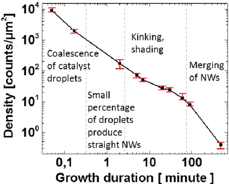
3.3.1. Droplets engineering ... 45
3.3.2 NW growth process ... 51
3.3.3 Hexagonal diamond crystalline SiNW ... 66
3.4 Summary ... 75
x
Chapter 4 SiGeNW and GeNW growth ... 81
4.1 Introduction ... 82
4.1.1 Why we study SiGeNWs ... 82
4.1.2 The state of the art of the SiGeNW and GeNW synthesis ... 82
4.2 SiGeNW and GeNW growth ... 83
4.2.1 Growth of SiGeNWs at 400°C ... 83
4.2.2 Increasing the Ge content of the SiGeNWs ... 86
4.2.3 GeNW growth at high temperature ... 91
4.3 Properties of SiGeNWs and GeNWs ... 99
4.3.1 Ge content studied by Raman and EDX ... 99
4.3.2 Crystallinity and chemical composition studied by TEM ... 102
4.3.3 Electrical and Optical properties studied by photoluminescence and absorptance measurements ... 107
4.4 Summary ... 109
References ... 110
Chapter 5 Towards low cost NW based radial junction solar cells ... 115
5.1 Introduction ... 116
5.2 Fabrication and characterization of NW radial junction solar cells ... 116
5.3 The performance of NW radial junction solar cells ... 122
5.3.1 SiNW based NW radial junction solar cells ... 122
5.3.2 SiGeNW based NW radial junction solar cells ... 130
5.4 Summary ... 132
References ... 132
Summary ... 137
Perspectives... 138
Annex I: Electrical modeling of nanowire radial junction solar cells ... 141
List of publications ... 155
Résumé ... 157
Chapter 1 Introduction
Contents
1.1 Let there be light ... 2
1.2 A new era of using light ... 4
1.3 Boost the solar cell performance by nanotechnology ... 7
1.4 Outline of this thesis ... 8
1.1 Let there be light 2
1.1 Let there be light
And God said, “Let there be light”, and there was light. Why light comes before human? This question can be answered from an energy point of view. Because through almost the whole human history, the energy needed for each movement of human comes indirectly or directly from light.
Since the first human, let’s call him Adam, till the beginning of the industrial revolution, the food and the wood provide almost all the energy we need. These energies eventually come from sunlight, which has been fixed into the organic matter such as plants by photosynthesis processes, as shown in figure 1.1. People may also use other kinds of energy from nature, such as water power and wind power. But these energies also come from sunlight, because the circulation of wind and water is driven by the heating of sunlight.
Figure 1.1. Photosynthesis process. The energy from the sunlight is fixed into organic matters, such as the plants, during the photosynthesis process. Photo from website www.wisegeek.com1.
With the development of society, humans have increasing abilities and activities. We enlarge and multiply our activities by using machines, especially since industrial revolution, as shown in figure 1.2 a. However, these powerful machines require big amounts of fuel for their engines. The amount of energy in these fuels is much bigger than the energy in the food we eat and the wood we burn. Fortunately, the sunlight has already prepared a solution for us. The energy of sunlight stored in the organic matters has been accumulated during billions of years in the form of fossil fuel. We just need to take these fossil fuels out of the earth and release the energy to support the rich and colorful modern life. Figure 1.2 shows the global energy consumption from 1850 to 2013. Now, we are using these fossil fuels at an extremely fast rate. With such a rate, we can finish the fuels formed during billions of years within next 100 years. Such a fast consumption rate also brings numerous problems to our society. Among the most serious ones are global warming and climate change. This is because huge amount of CO2 is released into the atmosphere when we burn the fossil fuel. This gas warms
the earth by making it to absorb more energy from the sunlight. If we continue to emit CO2 at the
current rate, the sea level might rise at meter scale2,3. The second problem is the pollution. Dust and other pollutants, which have negative effect on human health and environment, are also emitted to the atmosphere when burning fossil fuels. If the fossil energy keeps on dominating the energy production, a blue sky will be a luxury dream soon.
Figure 1.2. a) World energy consumption form 1850 to 2012. Photo from IIASA4. b) Illustration of the scale of different forms of energy. The volume of the balls corresponds to the amount of the energy. They are: green ball: 2015 world energy consumption; violet ball: proven uranium reserve; blue ball: proven gas reserves; dark red ball: proven oil reserves; black ball: proven coal reserves; yellow ball: solar energy received per year by earth.
Another fundamental problem is that the fossil fuels are exhausting. World energy consumption in 2013 was around 0.6 zetta joule5(zetta = 1021). This is a huge amount of energy which has a similar magnitude with the different forms of proven reserves of energy in the earth. There are 21 zetta joule of coal6, 9 zetta joule of oil6, 7 zetta joule of nature gas7, and 0.6 zetta joule of uranium8. The amount of these energies corresponds to the volume of different balls in figure 1.2 b. If we only use the fossil energy and maintain the energy consumption at the rate of year 2013, the proved reserves will last less than 100 years. With yearly increasing energy consumption, the fossil fuel reserves will not able to meet our demand soon. In figure 1.2 b, there is a huge yellow ball which is several thousand times bigger in volume than the ball which corresponds to the yearly energy consumption of mankind. This ball corresponds to the energy we receive from sunlight each year. Its value is around 4000 zettajoule. It can be a nice solution of energy for the near future.
The amount of energy we consume each year is huge. But if we use this amount of energy to lift the total water on the earth which is around 1.3 zetta liters9, we can lift only 4 centimeters. The development of our society always provides more and more access to more and more people with bigger energy consuming activities. It’s hard to imagine the consumption of energy will stop increasing. The solar energy that our planet receives each year is around 4000 zettajoule. This is still a finite number. It is not difficult to imagine the energy consumption by human will exceed this number in the future. Firstly, man-made facilities can already have very big energy consumption rate. For example the European Extreme Light Infrastructure laser will have a 200 Petawatt power10, that
1.2 A new era of using light 4
is bigger than the 174 petawatt total power Earth receives from the Sun. Secondly, individual can have huge energy consumption activity in the future. For example, people may have space-cars for high speed travel. These space-cars might have a higher energy consumption rate than rockets, which is in 100 GW scale11. This rate is millions times bigger than the current human average energy consumption rate, which is in the KW scale. Solar energy will not provide the ultimate solution to our energy needs. The solution for the far future needs to be virtually limitless energy. This might be achieved by changing the mass to energy directly. In fact this is how sunlight is generated. In such a way, the mass required to power the world in 2013 is just equal to the mass of an elephant. In fact, mankind already used this technique to transfer mass to energy inside nuclear plants. However, the safety and waste are serious issues for this generation of nuclear technology. We are putting huge effort to look for new ways to do the transfer. The multibillion euro international research project ITER is an example. This project seeks to harness the fusion power which can provides us safe, non-carbon emitting energy. The new technology is expected to be in use in several decades.
From now to the time when we find ultimate solution to our energy needs, it may take several decades or even hundred years. In this period, we need to face the increasing energy demand, serious problems brought by fossil fuel and the exhausting of fossil fuel. We need to find a clean and abundant energy, we need to change the energy structure. Once again, we look at the sun.
1.2 A new era of using light
Each year, a huge amount of solar energy is received by the earth. In order to use it, we have to change it to another form which can be used by our devices, for example electricity. To transform light to electricity, one option is to do the transition indirectly through mediums like wind and water. In this way, firstly sunlight heats the air and water, and then the air and water start to circulate. The movements of the wind and water rotate the turbines of the power generators to generate electricity. These are clean ways to generate electricity and have been well developed. In 2014, there are around 6800 GW of installed electricity generation capacity worldwide7, while hydropower is around 1200 GW12, and wind power is around 400 GW13. Since this is a different topic, we will not talk about it in detail. Here we will talk about another technology which has also reached a level of industrial maturity: photovoltaic solar energy.
A solar cell is a device which converts the sunlight into electricity directly. When the sunlight hits on a solar cell, the solar cell absorbs the energy of the light and gives it to its electrons to generate free electrons. Then the solar cell conducts the free electrons to flow to the power grid to form part of electricity we use. Figure 1.3 illustrates how a roof solar panel generates electricity for home use and power grid. In fact, the electric current generated by solar panels is direct current (DC), while in the power grid it is alternating current (AC), so an inverter is needed to convert the current from solar panel to AC current before home use or injecting to the grid.
Solar cells bring a revolution on using sunlight, because they convert it into electricity in a clean, efficient and direct way. Solar energy has a lot of merits when comparing with other forms of energy. It is clean and no CO2 involved during the energy production. These are the fundamental advantages
compared with fossil fuels. Compared with the nuclear energy, it does not have security and waste issues. It doesn’t have negative impact on biological and geological systems as hydro power. It does not have moving parts as wind power, thus it does not generate noise and requires less maintenance during operation. The capacity of solar panels depends on its size, which can be easily changed from
milliwatt to kilowatt scale. Therefore its installation can vary from small electrical devices, to house roofs, and to GW scale solar farms. What’s more, solar energy has a good public acceptance. It is one of the best candidates to provide the energy for the near future. The main challenge of solar energy is that we do not have sunlight at one place all the time. But there are many solutions. One is to use ultra-high-voltage (UHV) electricity transmission to connect the electricity generated at different places. In China, the single UHV line can be longer than 2000 Km. The UHV transmission lines in operation and under construction by state grid corporation of China are over 190 thousand kilometers14. These power lines can surround earth several times. In fact, the state grid corporation of China already planned worldwide power grid which will cost a 50 trillion dollar15,16. Once the whole world is connected, there is always electricity generated by sunlight at some place of the earth. Beside power grid, another solution is to store the extra electricity in the storage medium such as battery.
Figure 1.3. a) Working principle of solar cells, photo form website of Whittington Solar energy CO.17b) Real solar panel shown by students, photo from website of NREL18
The first solar cell can be dated to 1839, when French physicist demonstrated the photovoltaic effect and built the world’s first photovoltaic cell19. One of the early remarkable demonstrations of solar cells is from 1956, when researchers in Bell Laboratories demonstrated photovoltaic devices with energy conversion efficiency around 6%20,21. It means that the device can convert 6% of energy of the coming light into electricity. After several decades of efforts, this number increased to more than 46%. However, these high efficiency solar cells are very expensive. Thus they cannot be used at large scale. The technologies which have reached a level of industrial maturity are crystalline silicon solar cells and a few types of thin film solar cells. The best efficiency solar panels made of these solar cells have an efficiency around 24.4%22. The application of the photovoltaic solar energy has already achieved a great success. Till 2015, 226 GW of solar power electricity generation has been installed worldwide23. This represents around 3% world electricity generation capacity. China, the world’s largest consumer of energy and one of the most important source of growth for global energy demand, has achieved 43 GW of installed capacity, with 15 GW installed in 201524. According to International Energy Agency’s forecast, 4600 GW of installed PV capacity will be achieved by 2050, 16% of global electricity will generated by PV,25 as shown in figure 1.4.
1.2 A new era of using light 6
Figure 1.4. Forecast of PV electricity production from 2015 to 2050 under IEA’s high-renewables scenario25. The different colors correspond to different regions. The green curve on the top shows the share of total electricity. The black curve corresponds to the share of total electricity under IEA’s 2°C scenario.
The future of the solar energy is bright and exciting. However, it still costs more to use photovoltaic solar energy than other forms of energy. To install 4600 GW solar energy system, it will cost several trillion dollars. This is several times of France’s GDP in 2015. Reduction of the cost of solar energy systems can lead to huge savings. One of the most efficient ways is to increase the solar cells efficiency while maintaining or even decreasing the fabrication costs. This is because for a same PV system, if the solar cells efficiency is increased, the power output will increase significantly without increasing the system cost significantly. Thus the cost of per installed power capacity is decreased. First let’s look at the possibility to increase the efficiency of the current cells in the market. Current PV market is dominated by crystalline silicon solar cells. The theoretical efficiency limit for this kind of solar cells is around 30%26,27. Now the best cell efficiency has already achieved 26.3%22. This efficiency is very close to the limit. This makes it very difficult to further improve the efficiency. By the way, during the past 20 years, enormous efforts have been made to improve the crystalline silicon solar cell record efficiency, but only 2.3% efficiency improvement has been achieved22,28. To increase efficiency, researchers have also tried to use other materials to fabricate solar cells. These materials include inorganic compound GaAs8, CdTe and CuInGaSe, and organic compounds CH3NH3PbCl329. Among these kinds of solar cells, only GaAs solar cells have efficiencies better than
c-Si solar cells, which is around 29%. However, this kind solar cells has a higher fabrication cost than silicon solar cells. It is not suitable for large scale applications yet.
The main reason why solar cells have efficiency much lower than 100% is that they do not match the sunlight spectrum very well. We know that sunlight has many colors. Normally, one material can only absorb one color efficiently. If we want to absorb all the sunlight efficiently, theoretically we should use an infinite number of materials. However, technically it gets more difficult when the number of materials increases. For the moment, 34.1 %, 44.4% and 46% record efficiencies have been achieved for solar cells with 2, 3 and 4 absorbing materials, respectively. However, these solar cells are expensive. This is mainly due to the high materials cost and high cost of fabrication processes. Thus
high efficiency solar cells with combined absorbing materials are very attractive. Is it possible to fabricate them at low cost? One answer to this question is to use nanotechnology.
1.3 Boost the solar cell performance by nanotechnology
The nano in ‘Nanotechnology’ refers to nanometer scale. 1 nanometer is 109 times smaller than 1 meter. How small is 1 nanometer? The difference between 1 nanometer and 1 meter is same as the difference between the smallest particle we can see by our naked eye (~100 µm) and the size of the Paris region (~100 Km). Nanometer scale is just one of the plenty length scales of space, as shown in figure 1.5. Modern physics suggest that length can range from Planck length, which is around 1.6 x 10⁻³⁵ m, to the size of the observable universe, which is around 8.8 x 1026 m. Theoretically, the size of the object can be any value between the two size limits. We know that all the objects are composed of elementary particles. If we say the ultimate of the science and technology is to understand, identify and modify each elementary element up to Planck length scale, then we can say that the nanoscience and nanotechnology is to understand and modify the elementary particles or cluster of elementary particles at nanometer scale. This is an attractive ability. However, we human do not have this kind of ability naturally, because the smallest object our naked eye can see is around 100 µm. So naturally we do not manipulate with very small stuff, or we do not pay attention to them. Since thousands of years ago, people have invented lens which can zoom the image of the object. But till now, the best lens can only allow us to see objects with µm scale, not nm scale. In 1895, Wilhelm Röntgen discovered the X-ray, and in 1924 Louis de Broglie discovered the wave property of electron. These two discoveries allow the invention of X-ray tools and electron beam tools. These tools bring our vision from µm scale to nm scale. The concepts of nanotechnology came up soon after the advance of the microscope tools. In 1959, famous physicist Richard Feynnam considered the possibility of manufacture things atom by atom30. Generally, people consider that the starting of nanotechnology age is the beginning of 1980s, when scanning tunneling microscope and atomic-force microscopy was invented. These tools allow us to modify material at nanoscale. Nowadays, nanotechnology is familiar to society. It is studied in various domains such as physics, chemistry, and biology. It is also commonly used in semiconductor industry. Since 1989, the semiconductor manufacturing processes enter nanometer scale31.
Figure 1.5. Length scale of the Universe. The nanoscale is marked in red. Photo from website32 Among the nanotechnology research teams, there is a group of researchers who study nanowires. Nanowire is a wire like object with diameter in the nanometer scale. The research on nanowires was started in 1964 by Ellis and Wagner, they have observed the catalyst induced nanowire growth33. Since 199834, the nanowire research gets increased interest, and from 200535, researchers start to
1.4 Outline of this thesis 8
use nanowires to fabricate solar cells. Figure 1.6 shows the image of a germanium nanowire acquired by scanning electron microscope. This nanowire has a diameter of 60 nm and a length of 1600 nm. Nanowire structure has many advantages for solar cells application. Firstly, in nanowire solar cells, the light absorption direction is along axial direction, while the electrons and holes generated in the solar cell are collected in the radial direction. Since the distance in the radial direction is nanometer scale, the carriers can be collected efficiently even with low quality materials. This means that high efficiency solar cells can be made with low cost materials and low cost fabrication process. Secondly, the size of the nanowire solar cells is in the similar length scale with the wavelength of the visible light, which contains the majority part of the energy of sunlight. The similar length scale makes the nanowire structure to interact strongly with light. Thus only small amount of material is needed to absorb the incoming light. Lastly, at nanometer scale, the materials can exhibit novel properties such as discrete band structure, ballistic transport, quantum confinement and novel crystalline structures.
Figure 1.6. SEM image of a germanium nanowire grown by plasma-assisted VLS method. This NW is 60 nm in diameter and 1600 nm in length.
1.4 Outline of this thesis
The purpose of this research is to explore the potential of nanowire based radial junction solar cells theoretically and experimentally. Firstly, to find out the maximum light absorption of different solar cell configurations, we have performed optical simulation. Then to get a good understanding of the carrier transport, an electrical model for radial PN junction NW solar cells has been developed from first principles. Then the work has switched to the experimental part. We have carried out a detailed analysis of the plasma-assisted Vapor Liquid Solid Si nanowire growth process. In order to develop low bandgap and high mobility materials for multi-junction solar cells applications, we have grown SiGe and Ge nanowires in the same PECVD reactor used for Si nanowire growth. Finally, single and tandem junction solar cells have fabricated based on the Si and SiGe nanowires. The work will be presented in the following sequence:
Figure 1.7. Representative pictures for chapter 2 to 5.
Chapter 2. Optical modeling of nanowire radial junction solar cells
This chapter starts with the theoretical back ground of the light and material. Then it follows with the general knowledge of simulation with Comsol software. After that, the optical simulation of nanowire radial junction solar cells with different configurations will be presented.
Chapter 3. Si nanowire growth
This chapter provides a detailed information of the Si nanowire growth using a plasma-assisted Vapor Liquid Solid process. It starts with the introduction of the experimental setups involved in the study. Then it follows with the results of catalyst droplets engineering. The major part of this chapter is the detailed observation and explanation of the Si nanowire growth process. The rare hexagonal phase of Si has been observed in the as grown Si nanowires will also be presented.
Chapter 4. SiGe and Ge nanowires growth
In the first part of this chapter, we will show how to vary the growth from Si nanowires to SiGe nanowires, and finally to Ge nanowires. We will explain the influence of substrate temperature, gas partial pressure ratio and catalyst on nanowire growth. The growth of micrometer long and cylindrical Ge nanowires will be also presented. In the second part of this chapter, we will present the Ge concentration, crystallinity, optical and electrical properties of the SiGe and Ge nanowires. Chapter 5.
Towards low cost NW based radial
junction solar cells
In this chapter, firstly the synthesis and characterization of nanowire radial junction solar cells will be introduced. Then the performance of single and tandem solar cells with different absorber materials, including the first SiGe nanowire based solar cells, will be presented.
References 10
References
1 What is Photosynthesis, wiseGEEK. Retrieved June 20, 2016, from
http://www.wisegeek.com/what-is-photosynthesis.htm.
2 US Global Change Research Program. Climate Change Impacts in the United States: The Third National Climate Assessment(PDF). National Climate Assessment. 3rd Assessment: pg. 45. Retrieved 12 December 2015.
3 Levermann, A. et al. The multimillennial sea-level commitment of global warming.
Proceedings of the National Academy of Sciences 110, 13745-13750,
doi:10.1073/pnas.1219414110 (2013).
4 Nakicenovic, N. The Global Energy Assessment: Toward a Sustainable Energy Future, IIASA, 2012. Retrieved June 23, 2016, from
http://www.iiasa.ac.at/web/home/resources/mediacenter/FeatureArticles/Sustainable.en.ht
ml.
5 iea 2015 Key world Energy statistics. Retrieved June 23, 2016, from
http://www.worldenergyoutlook.org/.
6 Energy Study: Reserves, Resources and Availability of Energy Resources 2015, BGR (Federal Institute for Geosciences and Natural Resources), 2015. Retrieved June 23, 2016, from
http://www.bgr.bund.de/EN/Themen/Energie/energie_node_en.html.
7 CIA world fact book. Retrieved June 23, 2016, from www.cia.gov.
8 Colombo, C., Heiβ, M., Grätzel, M. & Morral, A. F. i. Gallium arsenide p-i-n radial structures for photovoltaic applications. Appl Phys Lett 94, 173108, doi:10.1063/1.3125435 (2009). 9 Total water on Earth, the Physics Factbook. Retrieved June 24, 2016, from
http://hypertextbook.com/facts/2001/SyedQadri.shtml.
10 The European Strategy Forum on Research Infrastructures 2016 Roadmap, European Commission. Retrieved June 24, 2016, from
http://ec.europa.eu/research/infrastructures/index_en.cfm?pg=esfri.
11 Kyle, E. NASA's Space Launch System Data Sheet, Updated July 5, 2016. Retrieved June 24, 2016, from http://www.spacelaunchreport.com/sls0.html.
12 IHA communications team, 33 GW new hydropower capacity commissioned worldwide in 2015. Retrieved June 24, 2016, from
http://www.hydropower.org/blog/33-gw-new-hydropower-capacity-commissioned-worldwide-in-2015#sthash.nrIoGGWI.dpuf.
13 Global Wind Report Annual Market Update 2014. GWEC. 22 April 2016. Retrieved May 23, 2016, from
http://www.gwec.net/wp-content/uploads/2015/03/GWEC_Global_Wind_2014_Report_LR.pdf.
14 State grid corporation of China, Yuheng-Weifang 1000kV UHV AC Transmission and Transformation Project Starts Construction, Released on 14-05-2015. Retrieved June 24, 2016, from http://www.sgcc.com.cn/ywlm/projects/ultrahighvoltage/05/325791.shtml. 15 SPEGELE, B. China’s State Grid Envisions Global Wind-and-Sun Power Network. Retrieved
June 24, 2016, from
http://www.wsj.com/articles/chinas-state-grid-envisions-global-wind-and-sun-power-network-1459348941. (2016).
16 Minter, A. China Wants to Power the World, Bloomberg. April 3, 2016. Retrieved June 24, 2016, from https://
www.bloomberg.com/view/articles/2016-04-03/china-s-state-grid-wants-to-power-the-whole-world.
17 How Solar Energy Systems Work, Whittington Solar energy CO. Retrieved June 24, 2016 from
http://www.whittingtonsolar.com/home/start-here/how-solar-energy-works/.
18 National Renewable Energy Laboratory. http://www.nrel.gov/. 19 Timeline of solar cells, Wikipedia. Retrieved June 24, 2016, from
https://en.wikipedia.org/wiki/Timeline_of_solar_cells.
20 Chapin, D. M., Fuller, C. S. & Pearson, G. L. A NEW SILICON P-N JUNCTION PHOTOCELL FOR CONVERTING SOLAR RADIATION INTO ELECTRICAL POWER. Journal of Applied Physics 25, 676-677, doi:10.1063/1.1721711 (1954).
21 April 25, 1954: Bell Labs Demonstrates the First Practical Silicon Solar Cell. APS News. American Physical Society. 18 (4). (2009).
22 Green, M. A. et al. Solar cell efficiency tables (version 49). Progress in Photovoltaics: Research
and Applications 25, 3-13, doi:10.1002/pip.2855 (2017).
23 2015 Snapshot of Global Photovoltaic Markets. report. International Energy Agency. 22 April 2016. Retrieved May 24, 2016, from
http://www.iea-
pvps.org/fileadmin/dam/public/report/PICS/IEA-PVPS_-__A_Snapshot_of_Global_PV_-_1992-2015_-_Final_2_02.pdf.
24 Statistics of solar energy in 2015, National Energy Admisistration of China. Retrieved June 25, 2016, from http://www.nea.gov.cn/2016-02/05/c_135076636.htm.
25 Technology Roadmap: Solar Photovoltaic Energy - 2014 edition.
26 Richter, A., Hermle, M. & Glunz, S. W. Reassessment of the Limiting Efficiency for Crystalline Silicon Solar Cells. IEEE Journal of Photovoltaics 3, 1184-1191,
doi:10.1109/JPHOTOV.2013.2270351 (2013).
27 Shockley, W. & Queisser, H. J. Detailed Balance Limit of Efficiency of p‐n Junction Solar Cells.
Journal of Applied Physics 32, 510-519, doi:doi:http://dx.doi.org/10.1063/1.1736034 (1961). 28 Green, M. A., Emery, K., Bücher, K. & King, D. L. Solar cell efficiency tables (version 5).
Progress in Photovoltaics: Research and Applications 3, 51-55, doi:10.1002/pip.4670030106
(1995).
29 Kojima, A., Teshima, K., Shirai, Y. & Miyasaka, T. Organometal Halide Perovskites as Visible-Light Sensitizers for Photovoltaic Cells. Journal of the American Chemical Society 131, 6050-6051, doi:10.1021/ja809598r (2009).
30 Feynman, R. There’s Plenty of Room at the Bottom, December 29, 1959. Wikipedia. Retrieved February 14, 2017, from
https://en.wikipedia.org/wiki/There's_Plenty_of_Room_at_the_Bottom. 31 Semiconductor device fabrication, Wikipedia. Retrieved June 25, 2016, from
https://en.wikipedia.org/wiki/Semiconductor_device_fabrication. 32 Size scales of the Universe. Retrieved June 26, 2016, from
http://hendrix2.uoregon.edu/~imamura/123/lecture-1/lecture-1.html.
33 Wagner, R. S. & Ellis, W. C. Vapor-Liquid-Solid Mechanism of Single Crystal Growth. Appl Phys
Lett 4, 89-90, doi:Doi 10.1063/1.1753975 (1964).
34 Tian, B. et al. Coaxial silicon nanowires as solar cells and nanoelectronic power sources.
Nature 449, 885-889 (2007).
35 Law, M., Greene, L. E., Johnson, J. C., Saykally, R. & Yang, P. Nanowire dye-sensitized solar cells. Nat Mater 4, 455-459 (2005).
Charter 2 Optical modeling of nanowire radial
junction solar cells
Contents
2.1 Introduction ... 14 2.2 Theoretical back ground of optical modeling ... 14 2.2.1 The light ... 14 2.2.2 The material ... 15 2.2.3 Characterization of the n and k of the material ... 17 2.2.4 The structure of the solar cells for optical simulation ... 20 2.2.5 Optical modeling with Comsol multiphysics... 21 2.3 Modeling of NW solar cells with different configurations ... 23 2.3.1 cSiNW on a Ag layer ... 23 2.3.2 Comparison of NW solar cells and planar solar cells ... 26 2.3.3 a-Si:H/µc-Si:H tandem solar cells ... 31 2.4 Summary ... 35 2.5 References ... 36
2.1 Introduction 14
2.1 Introduction
As explained in the first chapter, nanowires (NWs) have numerous advantages for solar cell applications1-5. Among them, a main one is that the NW structure strongly interacts with light4, which has been demonstrated both experimentally6-8 and theoretically9,10. Optical modeling is an effective way to gain insight into the interaction between light and solar cells. It also provides information for the device optimization. In LPICM, NW solar cells based on randomly oriented Si NWs have been studied since several years.11-13. These NW solar cells have core multi shell structure. In the literature,
large amount of optical simulation works can be found. However, big majority of them consider the NWs are composed of a single material14. These studies can give a good estimation of the maximum absorption of the solar cells, but the detailed absorption in each layer of the solar cells cannot be provided. There are few papers which investigate the detailed absorption in the core multi shell NW solar cells15,16. Among these works, single junction a-Si:H solar cell with varied nanowires length and intrinsic layer thickness17, nc-Si:H/a-Si:H tandem solar cells with balanced photo-current15, and single
junction a-Si:H solar cell with tilted wire axis18 have been studied. These works give a good starting of the theoretical analysis of core multi shell NW solar cells. However, core multi shell NW solar cell is a complex system with multi variables, such as the thickness and the material of each layer, the pitch and length of the wires, and the simplification method. Such a high order of freedom requires one to build the optical model according to the real structures.
This chapter starts with the fundamental knowledge of light, the interaction between light and the material, and the optical characterization of the material. Then detailed simulation results of different types of solar cells are presented. Finally, it ends with a brief summary.
2.2 Theoretical back ground of optical modeling
2.2.1 The light
What is light? There has been long debate between particle theory and wave theory before the development of Maxwell’s electromagnetic theory. Then people were convinced that visible light is just a certain kind of electromagnetic waves. However, the observations of black body radiation and the photoelectric effect made people realize that light is not just a wave, instead it has a wave-particle duality. It means that light is wave-particles, and it is also wave. This duality is at the core of this optical modeling part because light needs to be considered as a wave to describe its interaction with a material, while the particle nature of light must be used to convert the absorbed energy from the light to the energy of generated free electron-hole pairs.
The wave nature of the light can be described by Maxwell equations: 𝛻 ∙ 𝑬 = 𝜌 𝜀0 (2.1) ∇ ∙ 𝑩 = 0 (2.2) ∇ × 𝑬 = −𝜕𝑩𝜕𝑡 (2.3) ∇ × 𝑩 = µ0(𝜀0 𝜕𝑬 𝜕𝑡+ 𝑱) (2.4)
Where 𝛻 is the nabla symbol which denotes the three-dimensional gradient operator, 𝛻 ∙ is the divergence operator, 𝑬 is the electric field, 𝜌 is the charge density, 𝜀0 is the permittivity of the vacuum, 𝑩 is the magnetic field, ∇ × is the curl operator, µ0 is the permeability of the vacuum, and 𝑱 is the electric current density.
In the vacuum, there are no charges, thus equation 2.1 equals 0. The current density in equation 2.4 is also 0, then by combining equation 2.3 and 2.4, we can obtain the wave equation in the vacuum: ∇2𝑬 − µ 0𝜀0 𝜕𝟐𝑬 𝜕𝑡2 = 0 (2.5) Or, ∇2𝑩 − µ0𝜀0 𝜕𝟐𝑩 𝜕𝑡2 = 0 (2.6)
Since 𝑩 is linked with 𝑬 by equations 2.3 and 2.4, equations 2.5 and 2.6 are equivalent to each other. So one equation among equations 2.5 and 2. 6 is enough to describe the wave. One solution to this equation is,
𝑬(𝒓, 𝑡) = 𝐸0𝑒𝑗(𝒌∙𝒓−𝑤𝑡) (2.7)
Where 𝐸0 is the peak amplitude of the electric field, 𝑤 is the angular frequency, 𝑗 is imaginary unit, which is defined as 𝑗2= −1 and
𝒌 = 𝑤√µ0𝜀0 (2.8)
The speed of the wave is 𝑐 = 1
√µ0𝜀0≈ 3 ∗ 10
8 𝑚/𝑠 (2.9)
2.2.2 The material
The material is composed of nuclei and electrons. In the electric field, nucleus and electrons can feel the electric force because they are charges. Thus when the electromagnetic wave passes by the material, it induces oscillations to the nucleus and electrons. Since the nucleus are thousands times heavier than the electrons, they do not move much. On the contrary, electrons can gain the energy from the oscillating electric field and reduce the energy of the electromagnetic waves, and this is the absorption of the light by the material.
The interaction between light and material can be calculated by studying the dipole induced to the nucleus and electron system by the electric field. Figure 2.1 a) shows a nucleus and electron system without applied electric field. In this case, the average position of the electron cloud has the same position as the nucleus because the electron cloud is distributed uniformly around the nucleus. Once an electric field with magnitude E is applied to this system, as shown in figure 2.1 b), the initial electron cloud will be deformed, the average position of the electron cloud becomes 𝒓 refers to the nucleus. This 𝒓 induced a dipole 𝑷.
2.2 Theoretical back ground of optical modeling 16
Figure 2.1. Interaction of an electric field with a nucleus-electron system. a) Electron cloud distribute uniformly around nucleus. b) Electron cloud is deformed by the applied electric field 𝑬. The average position of the electron cloud becomes 𝒓 with respect to the nucleus, and this induces a dipole 𝑷. When a wave described by equation 2.7 passes by the nucleus-electron system, the magnitude of 𝒓 can be described as:
𝑟 = 𝑞𝐸0𝑒−𝑗𝑤𝑡
𝑚𝑒𝑤2+𝑗𝑚𝑒𝑟𝑤−𝐾 (2.10)
Where q is electron change, the capital K is the spring constant of the oscillating system, 𝑚𝑒 is the electron mass.
The total polarization within a volume of the material induced by the wave can be described as: 𝑷 = −𝑁𝑞𝒓 = 𝑁𝑞2/𝑚𝑒
𝑤02−𝑤2+𝑗𝒓𝑤𝐸0𝑒
−𝑗𝑤𝑡 (2.11)
Where N is the number of dipoles per unit volume, and 𝑤0= √
𝐾 𝑚𝑒−
𝑁𝑞2
3𝑚𝑒𝜀0 (2.12)
Then in a material with no free charge and no current, the electric field induced by a dipole should be considered in equation 2.4. This equation becomes:
∇ × 𝑩 = µ0𝜀0 𝜕𝑬 𝜕𝑡+ µ0
𝜕𝑷
𝜕𝑡 (2.13)
Then the wave equation becomes: ∇2𝑬 −𝑐12[1 + 𝑁𝑞2/𝑚𝑒
𝜀0(𝑤02−𝑤2+𝑗𝑟𝑤)]
𝜕𝟐𝑬
𝜕𝑡2 = 0 (2.14)
The solution to this equation still has the same form with equation 2.7,
𝑬(𝒓, 𝑡) = 𝐸0𝑒𝑗(𝑘0∙𝒓−𝑤𝑡) (2.15)
But the relation between wave vector 𝑘0 and 𝑤 changes to:
𝑤 =𝑛̃𝑐𝑘0 (2.16)
Where 𝑛̃ = √1 + 𝑁𝑒2/𝑚𝑒
Where 𝑛̃ is a complex number with complex form. We can denote it’s real part by n and its imaginary part by k. Then
𝑛̃ = 𝑛 + 𝑗𝑘 (2.18)
It can be seen that 𝑤 and 𝑘0 do not have linear relation any more, the wave becomes dispersive in the material.
Combining equation 2.15, 2.16 and 2.18 we can get: 𝑬(𝒓, 𝑡) = 𝐸0𝑒−𝑘
𝑤 𝑐𝒓𝑒𝑗(𝑛
𝑤
𝑐𝒓−𝑤𝑡) (2.19)
In this equation 𝑘 is the imaginary part of 𝑛̃.From equation 2.19 it can be seen that 𝑘 leads to the exponential decay of electric field intensity. This is very important to solar cells application because it determines the absorption of the material. n leads to the reduction of wavelength and wave velocity by n times. 𝑛̃ is called the complex refractive index of the material.
2.2.3 Characterization of the n and k of the material
Spectroscopic Ellipsometry measurement is a way to obtain 𝑛 and 𝑘 of a material. In an ellipsometry experiment, the objective is to measure the complex ratio of Fresnel coefficients, which is given by19 𝜌 =𝑟𝑟𝑝
𝑠 = 𝑡𝑎𝑛𝜓𝑒𝑥𝑝𝑖∆ (2.20)
Where 𝑟𝑝 is the complex Fresnel reflection coefficient for light polarized parallel to the incident plane, 𝑟𝑠 is the complex Fresnel reflection coefficient for light polarized perpendicular to the incident plane, and 𝜓 and ∆ are ellipsometry angles.
In our experiments, we use a phase-Modulated Ellipsometer UVISEL with a PSMA configuration which is shown in figure 2.2 b). Here P, S, M, and A stand for fixed polarizer, sample, modulator and fixed analyzer, respectively20. The signal we measured is:
𝑠(𝑡) = 𝑠0{1 + 𝐼𝑠sin(𝛿[𝑡]) + 𝐼𝑐cos (𝛿[𝑡])} (2.21)
With:
𝐼𝑐= sin[2(𝐴 − 𝑀)] [𝑠𝑖𝑛2𝑀(2𝑀(𝑐𝑜𝑠2𝜓 − 𝑐𝑜𝑠2𝑃) + 𝑠𝑖𝑛2𝑃𝑐𝑜𝑠2𝑀𝑠𝑖𝑛2𝜓𝑐𝑜𝑠∆] (2.22)
𝐼𝑠= sin[2(𝐴 − 𝑀)] 𝑠𝑖𝑛2𝑃𝑠𝑖𝑛2𝜓𝑠𝑖𝑛∆ (2.23)
Where 𝑃, 𝑀, and 𝐴 are the azimuth of the polarizer, the photo-elastic modulator and the linear analyzer with respect to the plane of incidence, respectively. 𝛿(𝑡) = sin (𝑤𝑡), 𝑤 is the angular rotation speed of the phase-modulator, 𝑡 is the acquisition time. For our measurements, the configuration is 𝑀 = 0°, 𝐴 = 45°, and 𝑃 = 45°. This is known as configuration II, and it gives:
𝐼𝑐= 𝑠𝑖𝑛2𝜓𝑐𝑜𝑠∆ (2.24)
𝐼𝑠= 𝑠𝑖𝑛2𝜓𝑠𝑖𝑛∆ (2.25)
However, when the measured 𝜓 is bigger than 45°, the sample will be also measured with configuration III, with 𝑀 = 45°, 𝐴 = 90°, and 𝑃 = 45°. In this case, 𝜓 will be taken from the
2.2 Theoretical back ground of optical modeling 18
measurement of configuration III, and ∆ will be taken from the measurement of configuration II, and it gives:
𝐼𝑐= 𝑐𝑜𝑠2𝜓 (2.26)
𝐼𝑠= 𝑠𝑖𝑛2𝜓𝑠𝑖𝑛∆ (2.27)
With equation 2.24 and 2.25, or 2.26 and 2.27, the ellipsometry angles 𝜓 and ∆ , and also 𝜌 in equation 2.20 can be calculated easily. Then the complex pseudo-dielectric function of the material can be calculated as:
< 𝜖 >=< 𝜖𝑟 > +< 𝜖𝑖 >= 𝑠𝑖𝑛2𝜙{1 + [(1 − 𝜌)/(1 + 𝜌)]2𝑡𝑎𝑛2𝜙} (2.28) Where 𝜙 is the angle of incidence.
Figure 2.2. a) General scheme of a standard ellipsometer. PAS is the polarization state analyzer20. b) A UVISEL ellipsometer with a PSMA configuration used in this study.
Among the materials we have used, the crystalline materials are already well characterized in the literature. On the contrary, the properties of amorphous materials are largely determined by their deposition conditions. Thus in this study we have studied the optical properties of the amorphous materials deposited in our lab.
To extract the material parameters from the ellipsometry measurement data, we use Tauc-Lorentz model for the fitting. In Tauc-Lorentz model, the imaginary part of the complex dielectric function 𝜖𝑖 is the product of Tauc’s dielectric function above the band edge6 and the 𝜖𝑖 obtained from the Lorentz oscillator model21. Tauc’s dielectric function above the band edge is:
𝜖𝑖,𝑇(𝐸) = A𝑇(𝐸 − 𝐸𝑔)2/𝐸2 (2.29)
Where A𝑇 is the tauc coefficient, and 𝐸𝑔 is the optical band gap. The 𝜖𝑖 obtained from the Lorentz oscillator model is:
𝜖𝑖,𝐿(𝐸) = 2𝑛𝑘 =
A𝐿𝐸0𝐶𝐸
(𝐸2−𝐸
Where A𝐿 is the strength of the 𝜖𝑖,𝐿 peak, 𝐸0 is the peak transition energy, and 𝐶 is a broadening term. The product of equation 2.34 and 2.30 is:
𝜖𝑖,𝑇𝐿(𝐸) = 1 𝐸 𝐴𝐸0𝐶(𝐸−𝐸𝑔)2 (𝐸2−𝐸 02)2+𝐶2𝐸2, 𝐸 > 𝐸𝑔 (2.31)
Where 𝐴 = A𝑇A𝐿. The real part of the complex dielectric function 𝜖𝑟 can be obtained by Kramers-Kronig integration, given by:
𝜖𝑟(𝐸) = 𝜖𝑟(∞) + 2 𝜋𝑃 ∫ 𝜉𝜖𝑖(𝜉) 𝜉2−𝐸2𝑑𝜉 ∞ 𝐸𝑔 (2.32)
Where 𝑃 is the Cauchy principle part of the integral, 𝜖𝑟(∞) is an additional fitting parameter. The integral gives the following expression21:
𝜖𝑟,𝑇𝐿(𝐸) = 𝜖𝑟,𝑇𝐿(∞) + 𝐴𝐶𝑎𝑙𝑛 2𝜋𝜁4𝛼𝐸 0𝑙𝑛 [ 𝐸02+𝐸𝑔2+𝛼𝐸𝑔 𝐸02+𝐸𝑔2−𝛼𝐸𝑔] − 𝐴𝑎𝑎𝑟𝑐𝑡𝑎𝑛 𝜋𝜁4𝐸 0 [𝜋 − arctan ( 2𝐸𝑔+𝛼 𝐶 ) + arctan ( −2𝐸𝑔+𝛼 𝐶 )] + 4𝐴𝐸0𝐸𝑔(𝐸2−𝛾2) 𝜋𝜁4𝛼 [arctan ( 2𝐸𝑔+𝛼 𝐶 ) + arctan ( −2𝐸𝑔+𝛼 𝐶 )] − 𝐴𝐸0𝐶(𝐸2+𝐸𝑔2) 𝜋𝜁4𝐸 ln ( |𝐸−𝐸𝑔| 𝐸+𝐸𝑔) + 2𝐴𝐸0𝐶𝐸𝑔 𝜋𝜁4 𝑙𝑛 [ |𝐸−𝐸𝑔|(𝐸+𝐸𝑔) √(𝐸02−𝐸𝑔2)2+𝐸𝑔2𝐶 ] (2.33) where 𝑎𝑙𝑛 = (𝐸02− 𝐸𝑔2)𝐸2+ 𝐸𝑔2𝐶2− 𝐸02(𝐸02+ 3𝐸𝑔2), (2.34a) 𝑎𝑡𝑎𝑛 = (𝐸2− 𝐸02)(𝐸02+ 𝐸𝑔2) + 𝐸𝑔2𝐶2, (2.34b) 𝜁4= (𝐸2− 𝛾2)2+𝛼2𝐶2 4 , (2.34c) 𝛼 = √4𝐸02− 𝐶2, (2.34d) 𝛾 = √𝐸02− 𝐶2/2, (2.34e)
The figure of merit used to evaluate the fit is20: 𝜒2 = 1 𝑁−𝑀−1∑ (𝜓𝑇ℎ𝑒𝑜𝑟𝑦−𝜓𝐸𝑥𝑝𝑒𝑟𝑖𝑚𝑒𝑡)2 𝜎𝜓2 + (∆𝑇ℎ𝑒𝑜𝑟𝑦−∆𝐸𝑥𝑝𝑒𝑟𝑖𝑚𝑒𝑛𝑡)2 𝜎∆2 (2.35)
Where N refers to the total number of experiment data points, M is the total number of fitted parameters. Each 𝜎 in the denominators corresponds to the estimated uncertainty.
Once the complex dielectric function is obtained, the 𝑛 and 𝑘 can be calculated easily by the following equations:
𝑛 = √√𝜖𝑟2+𝜖𝑖2+𝜖𝑟
2.2 Theoretical back ground of optical modeling 20
and
𝑘 = √√𝜖𝑟2+𝜖𝑖2−𝜖𝑟
2 (2.37)
An example of the material characterization is shown in figure 2.3. The sample is a thin hydrogenated amorphous SiGe (a-SiGe:H) layer deposited on a corning glass substrate. The optical structure used for fitting is shown in figure 2.3 a). This structure consists of a corning glass substrate, a thin a-SiGe:H layer and a roughness composed of a-SiGe:H and voids. The black dots in figure 2.3 b) show the imaginary part of the measured pseudo-dielectric function. Tauc-Lorentz model is used to model the a-SiGe:H. The fitted imaginary part of the measured complex pseudo-dielectric function is shown in figure 2.3 b) with red curve. Through the fitting, the parameters of the Tauc-Lorentz model of a-SiGe:H are obtained: 𝐸𝑔= 1.63 𝑒𝑉 , 𝜀∞ = 0.4 , 𝐴 = 219 , 𝐸0= 3.63 𝑒𝑉, 𝐶 = 2.36 . With these parameters, the n and k of the a-SiGe:H material are obtained and shown in figure 2.3 c).
Figure 2.3. a) The optical structure used for fitting. b) Imaginary part of the complex pseudo-dielectric function of the sample. c) The imaginary and real part of the complex refractive index, k and n, obtained from the fitting.
2.2.4 The structure of the solar cells for optical simulation
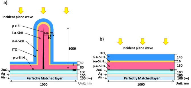
In this study, the main purpose the of the optical modeling is to achieve a good understanding of the interaction of the light and NW solar cells, and also to get information for the solar cell fabrication processes optimization. With such a goal, we have built optical models based on the solar cells structure we have fabricated. A top view SEM image of our solar cell is shown in figure 2.4 a). In this image, each wire is a solar cell which is composed of a p-type NW core, intrinsic absorber shell and a n-type shell. The NWs in this image are randomly oriented, and this brings a big challenge for the modeling. In order to simplify the problem, it is considered that the NWs are perpendicular to the substrate and have a square array arrangement. Figure 2.4 b) shows the top view of the simplified NW array, and figure 2.4 c) shows the detailed structure of each unite in figure 2.4 b). The pitch of NW array is usually around 1 µm. In figure 2.4 c), the axial direction of the NW solar cell is perpendicular to the substrate. The light is incident from the top along the normal direction. The boundary condition for the sidewall is Floquet periodicity. This cell has core multi-shell structure and the shells are layers of different materials and thicknesses. The boundary condition for the bottom surface is a perfect reflector. The space between NW solar cells is filled by air. For all the simulation of NW solar cells, we always use an infinite periodic array configuration, the axial direction of the NW
is perpendicular to the substrate, the light is incident from top plane along normal direction and with a power of 1 w for one cell. Floquet periodicity is used for four sidewalls.
Figure 2.4. a) Top view SEM image of the NW solar cells fabricated in our lab. b) Infinite periodic array of NW solar cells. c) One example of the structure of a NW solar cell unit used for simulation. 2.2.5 Optical modeling with Comsol multiphysics
As described before, optical modeling is used to study the interaction between the light and the materials. Since the structure of the material also plays an important role in the light matter interaction, there are three main elements in the optical simulation: light, material and structure. These three elements have been used as inputs of a commercial software (Comsol Multiphysics) to calculate the light absorption.
During the simulation, the main function of Comsol software is to solve the partial differential equations (PDE) which describe the light propagation in the material. In order to use finite element methods to solve PDE, the software firstly generates the mesh of the geometry and the weak form of the PDE. With the weak formulation, it is possible to discretize the mathematical model equations to obtain the numerical model equations. Then the software transfers the weak formulation, the boundary conditions and the meshed structure to matrix equations. After solving the matrix equations, some results can be visualized directly, such as the electric field. While some other results need post-processing. The calculation process is shown in figure 2.5 a). Figure 2.5 b) shows the mesh of a NW solar cell.
2.2 Theoretical back ground of optical modeling 22
The energy of the light which has been absorbed by the material can be calculated as: 𝑎𝑏𝑠 = 𝑐𝜀𝐸2
2 4𝜋𝑘
𝜆 (2.38)
Where 𝑐 is the speed of the light, 𝜀 is the permittivity of the material, 𝐸 is the electric field, and 𝜆 is the wavelength. To calculate the percentage of energy absorbed within a certain volume, one can integrate the absorption in this volume and normalize it by the total incident energy. The equation is shown below:
𝑃𝑎𝑏𝑠= ∭ 𝑎𝑏𝑠 4𝜋𝑘
𝜆 𝑑𝑣/𝑃𝑖𝑛𝑐𝑖𝑑𝑒𝑛𝑡 (2.39)
Where 𝑃𝑖𝑛𝑐𝑖𝑑𝑒𝑛𝑡 is the total incident power. To convert the absorbed energy to generated free electron, the particle nature of the light has to be used. As the light is composed of photons, the energy of each photon is a function of its wavelength:
𝐸𝑝ℎ𝑜𝑡𝑜𝑛= ℎ𝑐
𝜆 (2.40)
Where ℎ is the Planck constant. Equation 2.39 gives the ratio between absorbed energy by the material and the total incident energy as a function of wavelength. To calculate the number of absorbed photon when the material is exposed to the sun light, we can use this ratio to multiply the total photon number in the sun light at each wavelength. By assuming that each absorbed photon generates one free electron, the maximum photo-current can be calculated as :
𝐽𝑝ℎ𝑜𝑡𝑜𝑛= ∫ 𝑃𝑎𝑏𝑠(𝜆)
𝑊𝐴𝑀1.5(𝜆)
𝐸𝑝ℎ𝑜𝑡𝑜𝑛 𝑑𝜆 (2.41)
Where 𝑊𝐴𝑀1.5(𝜆) is the solar power spectrum.
The mesh size is a fundamental parameter for finite element methods calculation. A too big mesh size will lead to incorrect results, while a too fine mesh will lead to heavy computation and large memory requirements. In order to find the optimized mesh size for our problem, a series of simulations with varied mesh size has been done.
In this study, we consider an array of crystalline Si NWs sitting on the top of a silver layer. The SiNWs have a diameter of 200 nm and a length of 2 µm. the pitch of the NWs is 600 nm. The optical parameters for crystalline Si22 and Ag23 are from literature and are plotted in figure 2.6 b). We have changed the mesh size threshold to change the mesh number. As shown in figure 2.6 a), the mesh number changes from 5000 to 160000. The maximum theoretical short circuit current density has been calculated for these settings and is shown in Figure 2.6 c). It can be seen that when the mesh number is bigger than 20000, the change in the result is smaller than 5%. This mesh number corresponds to an average mesh volume of 45000 nm3, and an average mesh quality of 0.70. Where the mesh quality is calculated as:
𝑞 =(ℎ 72√3𝑉
12+ℎ22+ℎ32+ℎ42+ℎ52+ℎ62)3/2 (2.42)
Figure 2.6 a) NW solar cell with different mesh number. b) k value of c-Si and Ag at different wavelength. c) Maximum theoretical short circuit current density calculated with different mesh number.
2.3 Modeling of NW solar cells with different configurations
2.3.1 cSiNW on a Ag layer
In the literature, there are numerous reports of the synthesis of periodically arranged crystalline SiNWs, using top down methods7,24-26 and bottom up methods27. By inducing doping and a thin coating to form junction, these SiNW can be made to solar cells. Since the structure parameters such as pitch, length and diameter of these NWs can be changed easily, these structures can be optimized once the optimized parameters are known. To obtain the optimized parameters for NW solar cells, optical modeling is needed.
In this simulation, an array of crystalline Si NWs are placed on a 200 nm thick silver layer. The NW length is fixed to 3 µm, the pitch ranges from 500 nm to 700 nm, and the diameter ranges from 100 nm to 400 nm. The boundary condition for the bottom surface of the Ag layer is a perfect reflector.
2.3 Modeling of NW solar cells with different configurations 24
For crystalline Si solar cells, the photons which can be absorbed usually have a wavelength in the range from 300 nm to 1100 nm. Since the pitch of the NW array, the diameter and the length of NWs have the same order of magnitude of the wavelength, the light will propagate in the form of confined modes. Figure 2.7 shows the electric field in the cut plane which crosses the axis of the NW. The NW part and air part are inside and outside the white frame, respectively. From left to right, the pitch has increased from 500 nm to 700 nm. In figure 2.7 a) it can be seen that the pattern has a similar form when the pitch is increased from 500 nm to 700. However, the intensity decreases. This means that the confinement of energy in the NW decreases with the increase of pitch, and there is more and more leakage to the air. Figure 2.7 c) shows the absorptance of the NW arrays as a function of wavelength. The absorptance at 750 nm decreases with the increase of NW pitch. When the wavelength is increased to 900 nm, the NW array with 600 nm pitch has better light confinement, as shown in figure 2.7 b). In figure 2.7 c), it can be seen that NW array with 600 nm pitch has higher absorptance at 900 nm. This shows that one structure cannot have optimized light confinement for all the wavelength. With the increase of the wavelength, the pitch of the array should also increase to have a better light confinement.
Figure 2.7. a)-b), electric field distribution in SiNWs at different incident wavelengths: a) wavelength is 750 nm; b) wavelength is 900 nm. c) Absorptance of the NW arrays as a function of wavelength. The insets are electric field map of individual NW at wavelength 750 nm and 900 nm. The insets are from a) and b).
With equation 2.41, we have calculated the maximum theoretical Jsc for various configurations. The results are shown in figure 2.8. It can be seen that the values are in the range from 7 to 25 mA/cm2. When the NW diameter is 100 nm, the NW arrays with smaller pitch have a higher current. This is intuitive because the smaller pitch means bigger NW density and bigger material volume. But when the NW diameter is bigger than 300 nm, a 600 nm pitch gives the highest Jsc. Moreover, the increase