HAL Id: tel-01997230
https://pastel.archives-ouvertes.fr/tel-01997230
Submitted on 28 Jan 2019HAL is a multi-disciplinary open access archive for the deposit and dissemination of sci-entific research documents, whether they are pub-lished or not. The documents may come from teaching and research institutions in France or abroad, or from public or private research centers.
L’archive ouverte pluridisciplinaire HAL, est destinée au dépôt et à la diffusion de documents scientifiques de niveau recherche, publiés ou non, émanant des établissements d’enseignement et de recherche français ou étrangers, des laboratoires publics ou privés.
Mixed-signal predistortion for small-cell 5G wireless
nodes
Venkata Narasimha Manyam
To cite this version:
Venkata Narasimha Manyam. Mixed-signal predistortion for small-cell 5G wireless nodes. Electronics. Université Paris-Saclay, 2018. English. �NNT : 2018SACLT015�. �tel-01997230�
NNT
:
2018SA
CL
T015
Mixed-Signal Predistortion for Small-Cell
5G Wireless Nodes
Th `ese de doctorat de l’Universit ´e Paris-Saclay pr ´epar ´ee `a T ´el ´ecom ParisTech Ecole doctorale n◦580 Sciences et technologies de l’information et de la communication (STIC)
Sp ´ecialit ´e de doctorat : R ´eseaux, Information et Communications
Th `ese pr ´esent ´ee et soutenue `a Paris, le 09 Novembre 2018, par
V
ENKATAN
ARASIMHAM
ANYAMComposition du Jury :
Dominique Dallet
Professeur, Bordeaux INP Pr ´esident
Genevi `eve Baudoin
Professeur, ESIEE Rapporteur
Myriam Ariaudo
Maˆıtre de conf ´erences HDR, ENSEA Rapporteur
Philippe Meunier
Ing ´enieur, NXP Semiconductors France Examinateur
Patricia Desgreys
Professeur, T ´el ´ecom ParisTech Directeur de th `ese
Chadi Jabbour
Abstract
Small-cell base stations (picocells and femtocells) handling high bandwidths (> 100 MHz) will play a vital role in realizing the 1000X network capacity objective of the future 5G wireless networks. Power Amplifier (PA) consumes the majority of the base station power, whose linearity comes at the cost of efficiency. With the increase in bandwidths, PA also suffers from increased memory effects. Digital predistortion (DPD) and analog RF predistortion (ARFPD) tries to solve the linearity/efficiency trade-off. In the context of 5G small-cell base stations, the use of conventional predistorters becomes prohibitively power-hungry.
Memory polynomial (MP) model is one of the most attractive predistortion models, providing significant performance with very few coefficients. We propose a novel FIR memory polynomial (FIR-MP) model which significantly augments the performance of the conventional memory polynomial predistorter. Simulations with models extracted on ADL5606 which is a 1 W GaAs HBT PA show improvements in adjacent channel leakage ratio (ACLR) of 7.2 dB and 15.6 dB, respectively, for 20 MHz and 80 MHz signals, in comparison with MP predistorter. Digital implementation of the proposed FIR-MP model has been carried out in 28 nm FDSOI CMOS technology. With a fraction of the power and die area of that of the MP a huge improvement in ACLR is attained. An overall estimated power consumption of 9.18 mW and 116.2 mW, respectively, for 20 MHz and 80 MHz signals is obtained.
Based on the proposed FIR-MP model a novel low-power mixed-signal approach to linearize RF power amplifiers (PAs) is presented. The digital FIR filter improves the memory correction performance without any bandwidth expansion and the MP predistorter in analog baseband provides superior linearization. MSPD avoids 5X bandwidth requirement for the DAC and reconstruction filters of the transmitter and the power-hungry RF components when compared to DPD and ARFPD, respectively. The impact of various non-idealities is simulated with ADL5606 (1 W GaAs HBT PA) MP PA model using 80 MHz modulated signal to derive the requirements for the integrated circuit implementation. A resolution of 8 bits for the coefficients and a signal path SNR
2
of 60 dB is required to achieve ACLR1 above 45 dBc, with as little as 9 coefficients in the analog domain. Discussion on the potential circuit architectures of subsystems is provided. It results that an analog implementation is feasible. It will be worth in the future to continue the design of this architecture up to a silicon prototype to evaluate its performance and power consumption.
Acknowledgements
First and foremost, I would like to express my deepest and sincere gratitude to my supervisor Prof. Dr. Patricia Desgreys and co-supervisor Dr. Chadi Jabbour for entrusting me and providing me (an analog IC designer) with an interesting digital system challenge resulting in a nouvelle mixed-signal solution. Their unparalleled supervision at each step during the thesis has positively molded me and taught me many things for a lifetime, be it research methodologies, presentation skills or scientific writing. I feel immensely proud to have worked at T´el´ecom ParisTech on the future 5G telecommunications, where the word telecommunication was first coined by a T´el´ecom ParisTech alumni ´Edouard Estauni´e in the year 1904.
My sincere thanks to Dr. Dang-Ki`en Germain Pham for mentoring me and getting me started with the MATLAB codes. I have thoroughly benefited from his meticulous feedback and technical discussions during my thesis. I used to learn a new thing on each and every visit to his office.
I would also like to thank all the members of the jury, Prof. Genevi`eve Baudoin, Prof. Dominique Dallet, Dr. Myriam Ariaudo and Dr. Philippe Meunier for their invaluable feedback on my work. It is an honor to be able to have such experts in the jury. I was always inspired by their research work in this field.
I am particularly grateful to Prof. Yves Mathieu and Dr.Tarik Graba at the Safe and Secure Hardware (SSH) group at the COMELEC (Communications & Electronics) department for the help with RTL codes and digital ASIC implementation flow. I am very thankful to the faculty and colleagues at the COMELEC department, especially Circuits & Communications systems (C2S) group, Prof. Patrick Loumeau, Dr. Herv´e Petit, Dr. Hussein Fakhoury, Kelly Tchambake, Dr. Elias Solieman, Dr. Reda Mohellebi, Dr. Minh Tien Nguyen, Dr. Han Le Duc, Dr. Yosra Gargouri, Dr. Rapha¨el Vansebrouck, Dr. Ta Duc-Tuyen, Dr. Chetan Joshi, Dr. Manuj Mukherjee, Dr. Sumanta Chaudhuri for the interesting discussions and camaraderie.
4
Special mention goes to the head of the COMELEC department Prof. Bruno Thedrez, director of doctoral education Prof. Alain Sibille, Prof. Isabelle Zaquine for being my PhD r´ef´erent, Florence Besnard, Marianna Baziz, Chantal Cadiat, Yvonne Bansimba, Bernard Cahen and the HR team for the help with the administrative practicalities.
I would like to take this opportunity to thank all my teachers, professors and supervisors who have taught me and guided me since my early days at school. Special mention goes to my master thesis supervisor Dr. J Jacob Wikner at the Department of Electrical Engineering, Link¨oping University, for all the things he taught me from circuit design to scientific documentation.
I am extremely and eternally thankful to my parents, Durga Prasad and Vathsala for their unconditional love and support throughout my life. I especially thank my mother for imbibing in me the virtues of aim and ambition at an early age. Her untimely death during the final year of the PhD was a great personal loss to me. Though she is not with us today I still feel her warmth, and live with her teachings, blessings and memories. I dedicate this thesis to her.
I am grateful to my brother Sarath Chandra and his family. A big thanks to my friends Dhurv Chhetri, Suresh Siddagari, Anil K Balakrishnan and Lokesh Napa they have always inspired me and helped me during all the tough times.
Lastly, but by no means least, a big thanks to my dear wife Prasanna for all the love, affection and support. We are thankful to the god for gifting us a beautiful son Aasrith during the PhD tenure. His adorable smile cheered me up after all the long working nights. Special thanks go to Prasanna’s parents Murali Krishna and Gayatri, as well as to Pratyusha. They were always there to help us.
Contents
Contents 5
List of Figures 7
List of Tables 11
1 Introduction 17
1.1 Background on Wireless Systems . . . 18
1.1.1 5th Generation Mobile Networks . . . 18
1.1.2 Cellular Base Station Architecture . . . 19
1.1.3 Radio Frequency Transceiver . . . 21
1.1.4 Digital Modulation . . . 22
1.2 Background on Power Amplifier . . . 24
1.2.1 PA Metrics . . . 24
1.2.1.1 Efficiency . . . 24
1.2.1.2 Power Added Efficiency (PAE). . . 25
1.2.2 PA Behavior . . . 25
1.2.3 Nonlinearity Characterization . . . 26
1.2.3.1 Adjacent Channel Leakage Ratio. . . 26
1.2.3.2 Error Vector Magnitude (EVM) . . . 27
1.2.4 Effect of PAPR and nonlinearity on the efficiency . . . 28
1.3 Conclusion . . . 29
1.4 Specific Issues Dealt in This Work and Achievements . . . 30
1.4.1 Problem Statement and Thesis Objective . . . 30
1.4.2 Thesis Contributions and Organization . . . 31
1.4.3 Scientific Publications . . . 31
2 State-of-the-Art Predistortion Techniques 33 2.1 Introduction. . . 33
2.2 Outline of the PA Predistortion . . . 34
2.3 Digital Predistortion Methods . . . 35
2.3.1 Memory-Unaware Digital Predistortion (DPD) . . . 36
2.3.2 Memory-Aware DPD. . . 38
2.3.3 Advantages of DPD . . . 42
2.3.4 Disadvantages of DPD . . . 43
2.3.5 Conclusions on DPD . . . 44
2.4 Analog Radio Frequency Predistortion . . . 45
2.4.1 Memory-Unaware Analog Radio Frequency Predistortion (ARFPD) 46 5
6 CONTENTS
2.4.2 Memory-Aware ARFPD . . . 48
2.4.3 Advantages of ARFPD . . . 51
2.4.4 Disadvantages of ARFPD . . . 51
2.4.5 Conclusions on ARFPD . . . 51
2.5 Comparison of DPD and ARFPD . . . 54
2.6 Conclusion . . . 54
3 Algorithm Level Design and Digital Implementation 57 3.1 Introduction. . . 57
3.2 Predistorter Modeling . . . 58
3.2.1 Conventional memory polynomial predistorter . . . 58
3.2.2 FIR Memory Polynomial Predistorter . . . 60
3.3 PA Model Extraction Procedure . . . 61
3.4 FIR-MP Coefficient Identification Methodology . . . 70
3.5 Simulation Results, Optimal Dimensioning of DPD and DAC . . . 71
3.6 Digital Implementation of the Predistorter. . . 78
3.6.1 DPD fixed-point implementation . . . 78
3.6.2 Hardware synthesis. . . 80
3.7 Conclusions . . . 82
4 Mixed-Signal Predistorter System 85 4.1 Predistorter Modeling and Performance Comparison . . . 86
4.2 Mixed-Signal Predistorter Architecture . . . 88
4.3 Simulation with Major Non-idealities of APD . . . 91
4.4 Subsystems Architecture and Specifications . . . 94
4.4.1 Coefficient DACs . . . 96
4.4.2 Multipliers . . . 98
4.4.3 Time delays . . . 99
4.5 Conclusions . . . 103
5 Conclusions and Future Directions 105 A Principle of IMD cancelation in RF 121 B Digital ASIC Design Methodology 123 C MATLAB codes 125 C.1 Example MATLAB code implemented with persistent variables . . . 125
List of Figures
1.1 Illustration of cellular base station - a conventional macrocell network . . 20
1.2 Illustration of cellular base station - Heterogeneous Wireless Network (HWN) 20 1.3 Simplified block diagram of an Radio Frequency (RF) transceiver . . . 21
1.4 Constellation diagram for Quadrature Phase Shift Keying (QPSK) . . . . 23
1.5 Illustration of Power Amplifier (PA) input and output spectra . . . 26
1.6 Illustration of EVM . . . 27
1.7 Effects of distortion on QPSK constellation: (a) amplitude distortions,(b) phase distortions, and (c) combination of phase and amplitude distortions 28 1.8 Illustration of effect of Peak-to-Average Power Ratio (PAPR); output power and efficeincy vs. input power [1] . . . 29
2.1 Illustration of the principle of PA predistortion . . . 34
2.2 Illustration of a BS transmitter employing DPD system . . . 36
2.3 Gain based Look-Up Table (LUT) DPD of [2] . . . 37
2.4 LUT DPD indexed by average output control signal [3] . . . 38
2.5 Two-box DPD models (a) Wiener model and (b) Hammerstein model . . 40
2.6 Three-box DPD models (a) Wiener-Hammerstein model and (b) Hammerstein-Wiener model . . . 41
2.7 Block diagram of FLUT DPD of [4]. . . 42
2.8 3D plot of various DPD systems . . . 44
2.9 Illustration of a BS transmitter employing ARFPD system . . . 45
2.10 Block diagram of transmitter with ARFPD system . . . 46
2.11 LUT based RF predistorter of [5, 6] . . . 47
2.12 RFPD based PA driver stage of [7] . . . 47
2.13 Block diagram of the ARFPD system of [8] . . . 49
2.14 Block diagram of the FIR-EMP ARFPD [9, 10] . . . 50
3.1 Illustration of MP predistorter . . . 59
3.2 AM/AM plot without and with MP predistorter for a 4 carrier modulated signal with a total bandwidth of 80 MHz and PAPR of 8.4 dB . . . 59
3.3 Power spectra of the output without and with MP predistorter for a 4 carrier modulated signal with a total bandwidth of 80 MHz and PAPR of 8.4 dB . . . 60
3.4 Illustration of FIR-MP predistorter . . . 61
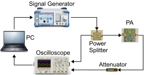
3.5 Measurement setup used for PA characterization . . . 62
3.6 Measured PA input and output RF data from the oscilloscope sampled at 20 GSPS. Plots on the left is for the total captured duration, i.e., 50 µs and on the right is the time-magnified data for 50 ns duration . . . 63
8 LIST OF FIGURES
3.7 Spectra of the measured PA input and output RF data captured from the oscilloscope. Spectra on the left is for the total captured frequency, i.e., from −10 GHz to 10 GHz and on the right is the frequency-magnified data from 1.75 GHz to 2.25 GHz . . . 64
3.8 Spectra of the measured PA input and output downconverted and power-aligned data. Spectra on the left is for the total captured frequency, i.e., from −10 GHz to 10 GHz and on the right is the frequency-magnified data from −250 MHz to 250 MHz . . . 65
3.9 Cross-correlation output plot. On the left is for the total correlation data samples, i.e., a sample less than two million samples (1999999) and on the right is the data obtained by magnifying around the center peak, from 999892 to 999936 cross-correlation output samples . . . 65
3.10 PA input and output baseband data envelope plots. Plots on the left is for the total captured duration, i.e., 50 µs and on the right is the time-magnified data for 50 ns duration . . . 66
3.11 AM/AM (left) and AM/PM plots (right) of the baseband signal data . . 66
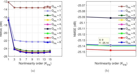
3.12 NMSE (dB) vs. KP A, for different QP A for the 20 MHz bandwidth signal
(a) KP A from 1 to 15, QP A from 0 to 4 and (b) magnified around KP A = 11 67
3.13 NMSE (dB) vs. KP A, for different QP A for the 80 MHz bandwidth signal
(a) KP A from 1 to 15, QP A from 0 to 8 and (b) magnified around KP A = 9 67
3.14 Plots of the measured and modeled PA output envelope. Plots on the left is for the total signal measurement duration of 50 µs and on the right is the time-magnified data for 50 ns duration . . . 68
3.15 Spectra of the measured and modeled PA output. Spectra on the left is obtained with a single spectrum for both measured and modeled data and the spectra on the right is obtained by averaging . . . 69
3.16 AM/AM (left) and AM/PM plots (right) of the measured and modeled PA output signal data . . . 69
3.17 Illustration of the coefficient estimation methodology for FIR-MP DPD . 70
3.18 Illustration of FIR filter coefficients learning. . . 72
3.19 Illustration of MP block coefficients learning. . . 72
3.20 Simulation testbench for the DPD . . . 73
3.21 ACLR1 (dBc) vs. K, for different Q in the 20 MHz bandwidth signal case with MP and FIR-MP (L=1) DPDs, clocked at (a) 5X and (b) 9X signal bandwidth . . . 74
3.22 ACLR1 (dBc) vs. K, for different Q in the 80 MHz bandwidth signal case with MP and FIR-MP (L=6) DPDs, clocked at (a) 5X and (b) 9X signal bandwidth . . . 75
3.23 Power spectra of the output before and after linearization for a 4 carrier WCDMA signal with a total bandwidth of 20 MHz and PAPR of 8.4 dB. ACLR1 improvement of 7.2 dB is obtained using FIR-MP. . . 76
3.24 Power spectra of the output before and after linearization for a 4 carrier modulated signal with a total bandwidth of 80 MHz and PAPR of 8.5 dB. ACLR1 improvement of 15.6 dB is obtained using FIR-MP. . . 77
3.25 AM/AM plot showing the gain distortion, without and with the different predistorters for the 80 MHz input signal. . . 77
3.26 Spectra of the output signal without DPD and with floating-point and fixed-point representations of 16 bits, 14 bits and 12 bits for 20 MHz signal 80
LIST OF FIGURES 9
3.27 Spectra of the output signal without DPD and with floating-point and fixed-point representations of 16 bits, 14 bits and 12 bits for 80 MHz signal 80
4.1 Simulation testbench for the DPD . . . 87
4.2 Power spectra of the output before and after linearization for a 4-carrier signal with a total bandwidth of 80 MHz and PAPR of 8.3 dB, using various predistorters . . . 88
4.3 Transmitter with proposed mixed-signal predistorter (MSPD), along with the signal spectra at different stages . . . 89
4.4 MP analog predistorter architecture implementation (VM: Vector Multipler) 90
4.5 ACLR1 vs. coefficient DAC resolution, for various signal path SNR values, for the case of K = 9 and M = 6 . . . 93
4.6 ACLR1 vs. coefficient DAC resolution, for various signal path SNR values, for the case of K = 5 and M = 2 . . . 93
4.7 Power spectra of the output before and after linearization using non-ideal FIR-MP predistorter, with K = 5 and M = 2 . . . 94
4.8 ACLR1 histogram obtained from 1000 runs of transient Monte Carlo simulations with 5% td mismatch . . . 95
4.9 Illustration of an N-bit binary-encoded charge-redistribution DAC [11] . . 97
4.10 Current-mode multiplier circuit of [12] . . . 99
4.11 The gain and phase transfer function of an ideal time delay cell [13] . . . 100
4.12 The block view of the first-order all-pass filter. . . 101
4.13 The gain and phase transfer function of a first order APF [13]. . . 101
4.14 The gain and phase transfer function of an ideal first order APF with td
of 1.4 ns . . . 101
4.15 The first order APF of [13] . . . 102
A.1 Illustration of predistortion signal generation for the case of two-tone signal.122
List of Tables
1.1 Base Station (BS) classification and their properties . . . 19
1.2 Spectral efficiency of various modulation schemes . . . 23
2.1 Survey of various DPD systems with various performance metrics. . . 43
2.2 State-of-the-art survey of predistortion systems . . . 53
2.3 Comparison of DPD and ARFPD in the context of small-cell BS with high bandwidth (≥ 100 MHz) . . . 54
3.1 Performance summary of MP and FIR-MP DPDs. . . 76
3.2 FIR-MP DPD performance summary for floating-point and various datap-ath wordlengths. . . 79
3.3 Digital implementation summary for the FIR-MP DPD . . . 82
4.1 Comparison of predistoter performance . . . 88
4.2 Predistorter coefficients of the simplified predistorter. . . 96
Acronyms
3GPP 3rd Generation Partnership Project AAF Anti-Aliasing Filter
ACLR Adjacent Channel Leakage Ratio ACPR Adjacent Channel Power Ratio ADC Analog-to-Digital Converter
AFE Analog Front End
AM Amplitude Modulation
APD Analog Predistortion
ARFPD Analog Radio Frequency Predistortion ASK Amplitude Shift Keying
BB Baseband
BBU Base-Band Unit
BS Base Station
BTS Base Transceiver Station
CA Carrier Aggregation
CC Component Carrier
CDMA Code Division Multiple Access CFR Crest Factor Reduction
CMOS Complementary Metal Oxide Semiconductor CPRI Common Public Radio Interface
DAC Digital-to-Analog Converter DAC Digital-to-Analog Converter DFT Discrete Fourier Transform DPD Digital Predistortion DSP Digital Signal Processing
EMP Envelope Memory Polynomial
EVM Error Vector Magnitude
FBMC Filter Bank Multi-Carrier 13
14 Acronyms
FDSOI Fully-Depleted Silicon-on-Insulator
FM Frequency Modulation
FSK Frequency Shift Keying
GaAs Gallium Arsenide
GaN Gallium Nitride
GMP Generalized Memory Polynomial HBT Heterojunction Bipolar Transistor
HD Harmonic Distortion
HPA High Power Amplifier
HWN Heterogeneous Wireless Network
ICT Information and Communications Technology
IF Intermediate Frequency
IM Intermodulation
IM3 Third-order Intermodulation IMD Inter-Modulation Distortion
IoT Internet of Things
IP3 Third-order Intercept point
IQ Inphase and Quadrature
ISI Inter-Symbol Interference
LNA Low noise Amplifier
LTE Long Term Evolution
LTI Linear Time Invariant
LUT Look-Up Table
MIMO Multiple-Input Multiple-Output ML-LUT Memory Less Look-Up Table
MP Memory Polynomial
MSPD Mixed-Signal Predistortion NMSE Normalized Mean Square Error
OBSAI Open Base Station Architecture Initiative OFDM Orthogonal Frequency-Division Multiplexing
PA Power Amplifier
PAE Power Added Efficiency PAPR Peak-to-Average Power Ratio
PD Predistortion
PM Phase Modulation
Acronyms 15
PSK Phase Shift Keying
QAM Quadrature Amplitude Modulation QPSK Quadrature Phase Shift Keying
RBS Radio Base Station
RF Radio Frequency
RFPD Radio Frequency Predistortion
RRH Remote Radio Head
SSAPI Small-Signal Assisted Parameter Identification
TNTB Twin Nonlinear Two-Box
TWT Traveling Wave Tube
UE User Equipment
UFMC Universal Filtered Multi-Carrier UHD Ultra High Definition
VGA Variable Gain Amplifier
WCDMA Wideband Code Division Multiple Access
NF Noise Figure
FFT Fast Fourrier Transform
FPGA Field Programmable Gate Array
AGC Automatic Gain Control
AWG Arbitrary Wave Generator PSD Power Spectral Density
LMS Least Mean Square
SFDR Spurious Free Dynamic Range
BW BandWidth
FS Full Scale
SNR Signal-to-Noise Ratio
SNDR Signal-to-Noise and Distortion Ratio FIR Finite-Impulse-Response
IIR Infinite-Impulse-Response
LPF Low Pass Filter
Chapter 1
Introduction
The phenomenal increase in the number of mobile devices, coupled with an exponential growth of the data traffic to support emerging applications, such as cloud storage and computing, over the past few years has led to an extensive increase in energy consumption by cellular networks. This scenario is expected to sustain or even exacerbate in foreseeable future. The energy consumption of the Information and Communications Technology (ICT) is expected to grow from 600 TWh in the year 2009 to 1700 TWh by the year 2030 [14]. This is around 3-4% of the total world electrical energy consumption [15, 14]. A significant portion (around a third) of it is consumed by the mobile communication networks.
Base stations are at the heart of these mobile communication networks, which account for more than 50% of the total network energy consumption [16,17,18], and can even be up to 85% [19]. The component which is still consuming the majority (60%) of the power in a base station is the power amplifier (PA) [20,21,22], which is a key block of the RF transceiver that delivers high power to the antenna. The increase in data rates calls for increased signal bandwidths, in excess of 100 MHz. While new spectrum bands are being added to the standards, the spectrum is still a scarce resource. This has led to cell densification, whereby efficient spectral reuse is possible. Low-power small-cell base stations, namely, picocells and femtocells, have been emerging as a natural choice to increase the network capacity, with a low cost of installation and operation when compared to the microcells and macrocells.
In this chapter, an introduction to the basic background concepts in wireless communica-tion systems and also the concepts related to the Power Amplifiers (PAs), are provided in Section1.1 and Section1.2, respectively. Conclusions for these two sections are provided in Section 1.3. The theory developed will be utilized in the subsequent section and
18 Chapter 1 Introduction
chapters. Finally, Section1.4 provides an overview of the issues dealt in this work along with the scientific achievements.
1.1
Background on Wireless Systems
The radio standards have evolved from pre-cellular mobile radio telephone (or 0G), to cellular fourth generation (4G) Long Term Evolution (LTE), with each cellular generation lasting approximately for a decade. 4G networks have hit the theoretical data rate limits for the contemporary technologies and cannot address the growing demands for data rates in a sustainable manner. Hence they have evolved towards 5G.
1.1.1 5th Generation Mobile Networks
5G mobile radio networks are slated to be deployed beyond 2020 [23]. Though the standards are not yet released, the main features of 5G would be to provide ubiquitous and seamless communications all the time, not just between humans but also between machine to machine and human to machine. The 5G networks should also provide baseline data rates for each user of around 1 Gbps and peak rates of up to 10 Gbps. This requires larger signal bandwidth available for each user, over 100 MHz [24]. This is enabled by advanced Carrier Aggregation (CA). For example, five Component Carriers (CCs) of 20 MHz can be aggregated to provide 100 MHz of spectrum to a single user. While the available radio spectrum is getting crowded and is increasingly looking scarce, the target for 5G is to achieve 1000 times more system capacity. Spectral efficient modulation schemes will be introduced, with a target to improve the spectral efficiency by 10 times. The problem of spectrum availability could be solved by utilizing new bands in sub 6 GHz and exploring centimeter/millimeter spectrum (6 GHz to 100 GHz band). Spectral reuse and Multiple-Input Multiple-Output (MIMO) techniques for spatial multiplexing within smaller cells (picocells and femtocells) will result in denser deployment. Apart from providing high data rates, the networks should also be energy efficient, reliable, provide low latency services and should support multitude of low power devices of IOT (Internet Of Things) and hence the networks should be highly energy-scalable. Backward compatibility and co-existence with legacy radio access technologies are nevertheless needed.
Chapter 1 Introduction 19
1.1.2 Cellular Base Station Architecture
Base Transceiver Station (BTS) or simply Base Station (BS), also known as Radio Base Station (RBS), node B in 3G networks and evolved node B (eNB) in 4G networks are at the heart of cellular communication networks. They are usually stationary installations of Base-Band Unit (BBU) and radio equipment, known as Remote Radio Head (RRH), containing transceivers with necessary electronic circuitry, Power Amplifiers (PAs) and antennas to facilitate communication between User Equipments (UEs) [25, 26]. The fronthaul connects the BBU andRRH using Common Public Radio Interface (CPRI) or Open Base Station Architecture Initiative (OBSAI) optical links, of whichCPRI is the most common one. The CPRIlinks are usually clocked at submultiples of 30.72 Mbps, since a basicCPRI frame rate is 3.84 MHz [25,26]. The network backhaul provides the necessary data and control information from the mobile switching center or the core network for transmission and reception to theBS. The network backhaul might be either an optical or a microwave link providing sufficient data capacity. Free-space optical communications is also emerging as an option for the 5G technologies [27]. The BSs are also the most power hungry subsystem of the cellular network, amounting to more than 50% of the total power consumption [28].
Based on the minimum coupling loss between the BSand the UE, four classes of base stations are defined by 3rd Generation Partnership Project (3GPP) in the present communication standards, as mentioned in Release 15 [29].
Table 1.1 presents the four classes ofBSs and the scenarios from which the classes are derived from. The Prated,c is the rated output power of the BS, which is defined as the
mean power per carrier at the antenna connector port during the transmission. The BSs can operate in single carrier, multi-carrier, or carrier aggregation configurations.
Table 1.1: BSclassification and their properties
BS class BS scenario Min. coupling
loss (dB)
Prated,C (dBm)1 Approx. max.
coverage radius
Wide area Macrocell 70 No upper limit ≤ 35 km
Medium range Microcell 53 ≤ 38 ≤ 2 km
Local area Picocell 45 ≤ 24 ≤ 200 m
Home Femtocell — ≤ 202 10m
1Nominal condition tolerance is ±2 dBm and extreme condition tolerance is ±2.5 dBm 2For one transmit antenna port. The rated power per antenna connector is accordingly scaled
with the number of transmit antennas, for example, Prated is ≤ 17 dBm for double transmit
antenna ports and < 11 dBm for eight transmit antennas, which is the maximum number of transmit antennas.
20 Chapter 1 Introduction
Figure 1.1: Illustration of cellular base station - a conventional macrocell network
Each of the BSclass mentioned in Table 1.1has its own purpose and properties. Wide area BS(macrocell) has been present since the inception of cellular communications and are commonly mounted on towers or rooftops of tall buildings for maximizing network coverage area, as shown in Fig. 1.1. The disadvantages of wide area BSs are high cost and power of operation, with the necessity for air-conditioning the High Power Amplifiers (HPAs), which by definition means any amplifier whose output power is greater than one Watt. Also, the users present at the edge of the cell have very weak signal strength. Later with the 2G the need for higher network capacity has called of microcells, which could serve densely populated localities needing extra network capacity, but with reduced radius of coverage and power. The aim is to utilize the spectrum efficiently by frequency reuse and reducing interference with proper frequency coordination.
Figure 1.2: Illustration of cellular base station - Heterogeneous Wireless Network (HWN)
Chapter 1 Introduction 21
Small cells, namely, picocells and femtocells, have been emerging as a natural choice to increase the network capacity, with low cost of installation and operation and without costly air-conditioning equipment starting with the 3G technology. The picocell form factor could be used to give network coverage to usually large indoor areas, where the signal strengths from macrocells and microcells are poor, like a big shopping mall, railway station, or a stadium, etc,. The femtocell goes a step further with even smaller power and coverage area, but is designed to efficiently cover small office or a home. The small-cells are inexpensive and easy to deploy when compared to microcells and macrocells, which are usually mounted on towers. The denser deployment of small-cells also improves the reliability, for example, in the case of failure of a femtocell, other nearby picocell can possibly serve the users momentarily, which could not be the case for a single macrocell scenario. The future 5G network architecture will be a combination of all the four classes ofBSs calledHWNs, or simply, Heterogeneous networks (HetNets) [30], as illustrated in Fig.1.2.
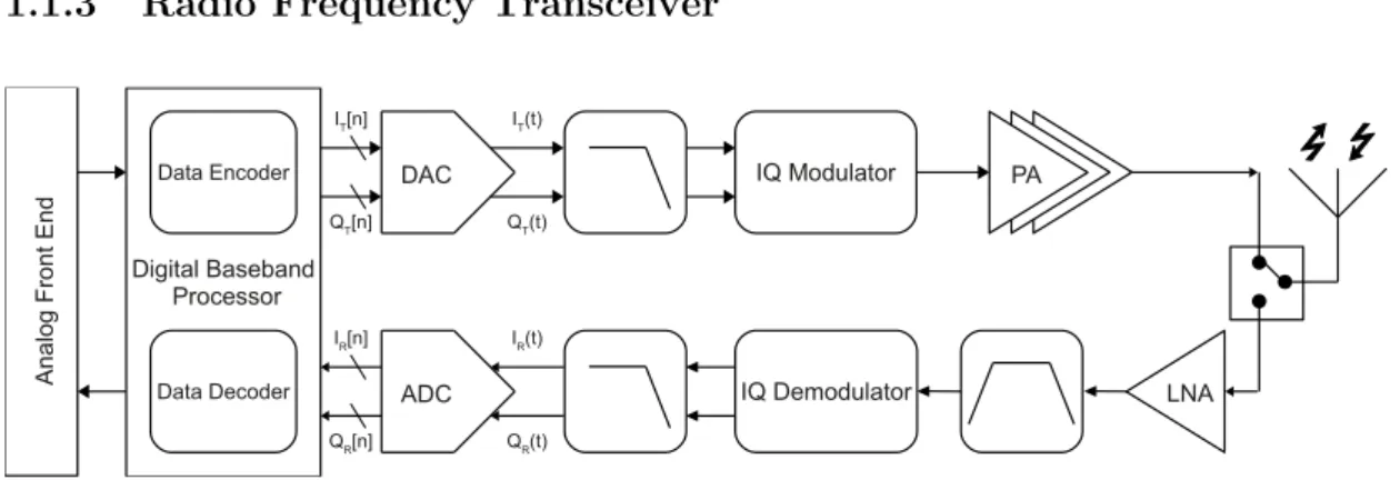
1.1.3 Radio Frequency Transceiver
Data Decoder Data Encoder Digital Baseband Processor A n a lo g F ro n t E n d QT[n] IT[n] DAC ADC IT(t) QT(t) QR[n] IR[n] IR(t) QR(t) IQ Modulator IQ Demodulator PA LNA
Figure 1.3: Simplified block diagram of an Radio Frequency (RF) transceiver
A simplified RF transceiver in the contemporary digital communications context is shown in Fig.1.3. In the transmit path, the Analog Front End (AFE) senses or acquires electrical equivalent signals, filters in analog domain and converts it to digital signals with the help of an Analog-to-Digital Converter (ADC). The sensors could be anything ranging from temperature sensor, to Ultra High Definition (UHD) video camera in the case of an User Equipment, or a photo diode for an optical backhaul of a BS. The digitized data is then processed in the digital baseband processor, doing necessary signal processing such as filtering, Discrete Fourier Transform (DFT), source encoding, channel encoding, etc. The source encoding does the compression of the data, and the channel coding introduces controlled redundancy which reduces the probability of error when the data is transmitted through the channel to be received by the receiver. Based on the digital modulation scheme the Inphase and Quadrature (IQ) data, IT[n] and QT[n],
22 Chapter 1 Introduction
of a zero IF transmitter, as considered here. Zero-IFor direct conversion architecture is one of the most used transceiver architectures [31]. The output signals of theDACs, IT(t) and QT(t), are then low-pass filtered using reconstruction filters also called
anti-imaging filters, to remove unwanted out-of-band noise and harmonics. An IQmodulator upconverts the complex baseband analog signal into real RF signal, which is usually followed by a Band Pass Filter (BPF). The RF signal to be transmitted is amplified by a PA, which is discussed in greater detail in Sec.1.2. The PA connects to the duplexer, which facilitates full-duplex operation avoiding the leakage of the transmitted signal into the receiver, and hence helps in avoiding two separate antennas, one for transmission and the other for reception. Finally, the antenna radiates the amplified RF signal into the free-space.
At the receiver end, the same antenna receives the desired reception signal with other unwanted signals at the same time. The received signal is processed in the reverse way, that is the signal is amplified, band selectively filtered, quadrature-downconverted to analog baseband and finally converted into digital domain, IR[n] and QR[n], by the
Low noise Amplifier (LNA),BPF,ADCpreceding with an Anti-Aliasing Filter (AAF), respectively. The digitized received data is processed and decoded by the same baseband processor. The received digital data can be stored or can be sent to the actuators, for example on to a screen for displaying information, with the help ofAFE.
1.1.4 Digital Modulation
Modulation is the modification of a carrier wave in accordance with the baseband data so that it is easy to transmit and receive properly. This can be accomplished by selectively modifying the sinusoidal carrier’s parameters, namely amplitude, frequency, and phase. All the modern communication systems employ digital modulation techniques, which are robust in comparison with their analog counterparts.
The basic digital modulation schemes are Amplitude Shift Keying (ASK), Frequency Shift Keying (FSK) and Phase Shift Keying (PSK), which are analogous to Amplitude Modulation (AM), Frequency Modulation (FM) and Phase Modulation (PM) in ana-log modulation, respectively. Advanced digital modulation schemes use quadrature modulation, for exampleQPSK, whose constellation is as shown in Fig. 1.4.
Gray coding is often employed to minimize the number of bits differing between two adjacent symbols, thereby minimizing the error probability. Spectral efficiency is the most important metric of any digital modulation scheme, which is described as the number of bits per second that can be transmitted over a bandwidth of one Hertz. Spectral efficiency of various modulation schemes are presented in Table1.2, [32,33].
Chapter 1 Introduction 23
00 10
01 11
Q
I
Figure 1.4: Constellation diagram for Quadrature Phase Shift Keying (QPSK) Table 1.2: Spectral efficiency of various modulation schemes
Modulation scheme Spectral Efficiency (bits/s/Hz) PAPR (dB)
BPSK 1 0
QPSK 2 0
8PSK 3 3.3
64QAM 6 3.7
OFDM ≥ 10 ∼ 12
1Can reach as high as 30 bits/s/Hz, depending on the number of subcarriers and
the modulation schemes for them
As can be seen in the Table 1.2, the OFDM is one of the most spectral efficient modulation schemes, which is used in 4G LTE. OFDM achieves this by employing multiple orthogonal subcarriers in a channel, each having its own modulation scheme (QPSK, 64QAM, etc.) and packing high amount of data in a given bandwidth. The orthogonality of the subcarriers avoids Inter-Symbol Interference (ISI). Orthogonal Frequency-Division Multiplexing (OFDM) is a synergistic combination of modulation and multiplexing technique. The other advantage of OFDMis immunity to multipath fading. For the case of 5G communications, other modulation formats such as Filter Bank Multi-Carrier (FBMC) and Universal Filtered Multi-Carrier (UFMC) are being looked at with advantages in comparison with OFDM [34,35,36].
24 Chapter 1 Introduction
1.2
Background on Power Amplifier
The power amplifier is the most important stage in the RFtransmitter, and is also the most power-hungry circuit not just in the transmitter, but also in the entire transceiver chain and in the BS[22,37]. It is the stage which prepares the low power radio signal coming form the IQ modulator by giving it as much power as possible from the DC supply, making it a high power signal to get transmitted into the free-space via antenna. The power gain of the PA is the ratio of the output power POut and the input power
PIn, given as:
Gain = POut PIn
. (1.1)
There are various classes of PAs with varying combinations of linearity and power efficiency [31,38,39]. Though from the definition perspective of an idealPA, only linear gain is assumed, in reality, depending on the PAclass of operation, various nonlinear effects comes into picture.
Coming to the choice of the RF power amplifier technology in the BSs, Gallium Nitride (GaN) and Gallium Arsenide (GaAs) were dominating the market till few years ago [39].
Now the silicon LDMOS technology is the leading choice, even for a small-cell BS
requiring upto few Watts, for its better performance and lower cost. It is a variant of the CMOS technology but is capable of delivering far more output power when compared to that of a normal CMOS device.
1.2.1 Generic PA Metrics
Apart from the power gain given by Eq.1.1, the following two metrics, namely, efficiency and Power Added Efficiency (PAE), are very important.
1.2.1.1 Efficiency
The foremost important performance measure of a PA is its efficiency, which is given by
ηP A=
PLoad
PSupply
, (1.2)
where PLoad is the power delivered to the load and PSupply is the power that the PA
Chapter 1 Introduction 25
the respective CMOS or bipolarPA implementations [31]. Ideally, the efficiency should be unity, where the entire power supplied to the PA should be delivered to the load. But in reality, depending on the class of PA operation and other practical reasons of physical implementations, like the limited output swing originating from the operating region of the power device, the efficiency is always below unity. Also note that this metric doesn’t take into account the gain of the amplifier.
1.2.1.2 Power Added Efficiency (PAE)
The other way to define the performance of the PA is by defining the PAEgiven by:
PAE = PLoad− PIn
PSupply
, (1.3)
where PIn is the power at thePAinput signal port.
PAEis important for aPA because the amplifier is mostly driven by another smaller amplifier in a tapering fashion for improved drivability and matching considerations. Hence we might note the following:
❼ The PAEis always smaller than the efficiency ηP A
❼ The better thePA input matching with the preceding stage, the higher thePAE. ❼ The higher the gain of the amplifier, the higher thePAE.
1.2.2 PA Behavior
PA input-output behavior can be categorized into three groups:
1. Memoryless (static) nonlinearities which is inherent to the power device. Taylor series expansion can be used to approximate the output behavior over some signal range: y(t) = N X n=1 anx(t)n, (1.4)
where x(t) is the input signal, y(t) is the output signal, anare the coefficients of
the polynomial, N is the nonlinearity order considered.
2. Linear memory effects which are memory behaviors uncorrelated with the nonlinear response of the power amplifier arising from time delays or phase shift
26 Chapter 1 Introduction
in the matching networks and can be modeled as Finite-Impulse-Response (FIR) filters.
3. Nonlinear memory effects come from linear circuits, such as capacitors, for example, combining with the nonlinear behavior of the transistor results in a term in the output signal of the power amplifier that includes a nonlinear function of different samples of the input signal at different instances [37].The other sources of nonlinear memory effects are direct low-frequency dynamics, such as trapping effects and non-ideal bias networks [22].
1.2.3 PA Nonlinearity Characterization Metrics
As previously mentioned the amplifier gain is nonlinear which results in the in-band signal degradation as well as unwanted emissions in other channels. The following section describes briefly the metrics used to measure thePA nonlinearity.
1.2.3.1 Adjacent Channel Leakage Ratio
PA input PA output (atten.) Frequency P o w e r S p e ct ra l D e n si ty Main Channel Lower Adjacent Channel Lower Alternate Channel Upper Adjacent Channel Upper Alternate Channel
Figure 1.5: Illustration ofPAinput and output spectra
ThePAnonlinearity can be characterized using Adjacent Channel Leakage Ratio (ACLR), also called as Adjacent Channel Power Ratio (ACPR), which gives us the measure of the extent to which the nonlinearly amplified modulated signal spreads to the adjacent and alternate channels in the frequency domain. Fig. 1.5shows a simple illustration of a modulated input and attenuated output spectrum of a PA, attenuated with a factor
Chapter 1 Introduction 27
of PA linear gain. The main channel is surrounded by similar bandwidth lower and upper adjacent and alternate channels respectively with guard bands in between. The main channel is the desired channel and is considered as the reference channel when calculating the ACLR, which is the power ratio expressed in dBc, and is given by
ACLR (dBc) = 10 log10 R BW PM ain(f )df R BWPAdjacent(f )df , (1.5)
where PM ain(f ) and PAdjacent(f ) are the Power Spectral Densities (PSD) in the main
channel and the adjacent channel respectively. It could be measured with respect to the alternate channel as well. The usual notation is ACLR1 U and ACLR1 L, when referring to upper and lower adjacent channels and ACLR2 U and ACLR2 L, when referring to upper and lower alternate channels.
Characterizing the spectral regrowth with the calculation of ACLR is one of the most important requirement, as each radio communication standard defines limits on spectral emissions with the help of the spectral mask, which should be abided by anyone who wants to communicate wirelessly in a specified licensed spectrum.
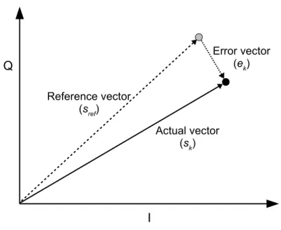
1.2.3.2 Error Vector Magnitude (EVM)
I
Q
Reference vector (sref) Actual vector (sk) Error vector (ek)Figure 1.6: Illustration ofEVM
The Error Vector Magnitude (EVM) is another nonlinearity measure which is used to quantify the PA nonlinearity. Contrary to ACLR, EVM describes the extent to which the nonlinearity of the amplifier degrades the inband quality of the modulated signal. The EVM is defined and calculated in the constellation domain, which because of nonlinearity
28 Chapter 1 Introduction
gets distorted and hence dispersed from its original position, as illstrated in Fig. 1.6. EVM is expressed in percentage and by definition is measured over one subframe in the time domain, which is 1 ms according to3GPP[29]. The formula forEVMcalculation is
EVM (%) = s PN k=1|ek|2 PN k=1|sref|2 , (1.6) where ek= sk− sref, (1.7)
where sref is the reference vector, sk is one of the N vectors present in one subframe,
which is obtained after nonlinear PA amplification and ek is the error vector.
Q
I
Reference constellation point Actual constellation point
(a)
Q
I
Reference constellation point Actual constellation point
(b)
Q
I
Reference constellation point Actual constellation point
(c)
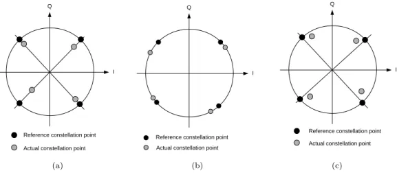
Figure 1.7: Effects of distortion on QPSK constellation: (a)amplitude distortions,(b) phase distortions, and(c) combination of phase and amplitude distortions
Fig.1.7illustrates the effects on PA nonlinearity on the signal constellation. NonlinearPA
can give amplitude distortion Fig.1.7(b), phase distortion Fig.1.7(a), or a combination of both amplitude and phase distortions Fig.1.7(c).
1.2.4 Effect of Peak-to-Average Power Ratio (PAPR) and PA
nonlin-earity on the efficiency
Linear amplification is desired for the modulation schemes based on amplitude modulation, where the modulated signal envelope also carries information. New spectral-efficient modulation schemes, likeOFDM for example. To achieve linear gain from the PA, the
PA should be “backed-off”, which means the whole input signal gets amplified only in the linear region of the PAwithout pushing it into nonlinear or saturation region. This significantly degrades the power efficiency of the PA. This is further exacerbated by the high PAPR, for example, in the case of OFDM,PAPRis very high around 12 dB
Chapter 1 Introduction 29
Figure 1.8: Illustration of effect of PAPR; output power and efficeincy vs. input power [1]
as shown in Table1.2. As shown Fig. 1.8, there exists a trade-off between the linearity and power-efficiency of the PA, which also has a dependency on signal PAPR. This makes the efficiency go below 10%, with the rest of the 90% power being dissipated in the power device. This calls for an advanced thermal management like expensive packaging, large heat-sink and air-conditioning. Therefore, it is to be noted thatPAPR
plays a very crucial role in the efficiency of the power amplifiers. Techniques such as Crest Factor Reduction (CFR) is usually employed to reduce the PAPR, at the cost of EVM degradation [25].
1.3
Conclusion
This chapter has presented the scenario of 5G mobile networks, where increasing number of low power small-cell BSs are going to play a vital role in the realization of cost and energy efficient ubiquitous communications. Radio frequency transceivers in the context of modern day communications utilize robust digital modulation techniques, like Quadrature Amplitude Modulation (QAM) andOFDM, and the preferred transceiver architecture is the zero-IF architecture. PA being the important stage of the transmitters is also the most power hungry block in the entireBS, whose efficiency comes at the cost of linearity. The important generic and nonlinearity metrics of the PA were introduced and the effect of PAPR and nonlinearity on the efficiency of the PAs was discussed.
30 Chapter 1 Introduction
1.4
Specific Issues Dealt in This Work and Achievements
1.4.1 Problem Statement and Thesis Objective
The PA suffers from a strong linearity/efficiency trade-off. The nonlinearities result in intermodulation distortions at the PA output which when transmitted cause spectral pollution, i.e., leaking a portion of transmitted power into the adjacent and alternate channels. Also, with the increased signal bandwidths the problem of memory effects has increased considerably, which results in dynamic nonlinearities. Additionally, new types of modulation schemes, such as OFDM, generate modulated signals with non-constant envelope resulting in high signalPAPR, further degrading the PA characteristic. In order to break this trade-off and increase the efficiency of the PA without linearity degradation, predistortion is usually employed. Predistortion corrects the PA nonlinearity and memory effects by generating approximate PA inverse characteristic to generate a fairly linear output at the PA. Predistortion can be done in analog [40,41], or digital [42,43], or even in the analog RF domain [8,10]. Owing to the robustness of digital signal processing, and benefits coming from the Complementary Metal Oxide Semiconductor (CMOS) technology scaling, Digital Predistortion (DPD) has become the de facto solution for the PA linearization [22,44].
Even though a plethora of DPD solutions have been proposed in the literature based on behavioral modeling, ranging from simple memoryless look-up table methods to complex neural networks, as summarized in [22, 45], they are specifically targeted towards macro-and micro-cell BS PAs, where the DPD power consumption is negligible when compared to that of the PA. Hence all the research effort has been made to obtain highly performant and robust DPD. Also, with the increasing bandwidths, employing a DPD, which usually has to handle at least five times the bandwidth of the signal in order to cancel out the distortion products, becomes excessively power-hungry. In the context of small-cell base stations the use of conventional DPD solutions becomes prohibitively power-hungry, and hence no DPD solutions are generally used until very recently [21, 22, 46]. Without a DPD, the PA suffers from poor power efficiency as the PA is usually backed-off to operate in linear regime. New modulation schemes tend to show high PAPR, and hence worsening the aforementioned problems.
The objective of the thesis is to develop low-power predistorter solutions suitable to linearize the small-cell base station PAs in the context of high bandwidth input signals. In particular, we are interested in developing a simplified predistorter model that can be employed not just in DPD implementations but also in analog and mixed-signal based implementations, which are emerging as alternatives in the context of small-cell PA predistortion.
Chapter 1 Introduction 31
1.4.2 Thesis Contributions and Organization
The thesis is organized in various chapters. A brief outline of it is as follows:
❼ Chapter2presents a brief literature review up to various state-of-the-art DPD and ARFPD solutions, which are again grouped into memory unaware and memory aware techniques. The chapter culminates with a discussion on various advantages and disadvantages of both the predistortion techniques and provides a comparison of them.
❼ Chapter3presents the developement of the FIR-MP model starting with the predis-torter modeling using conventional memory polynomial, detailing its shortcomings corroborated by MATLAB simulations. The digital implementation flow of the proposed FIR-MP algorithm in 28 nm Fully-Depleted Silicon-on-Insulator (FDSOI)
CMOStechnology and the simulation results obtained are presented.
❼ The architecture of the FIR-MP mixed-signal predistorter is presented in Chapter4. A brief analysis of the various non-idealities to derive the requirements of the circuit to be implemented using the proposed architecture is provided along with simulations.
❼ Finally, Chapter5provides concluding remarks and directions for the future work.
1.4.3 Scientific Publications
The thesis has resulted in the following scientific publications:
1. V. N. Manyam, D.-K. G. Pham, C. Jabbour, and P. Desgreys, “A low-power high-performance digital predistorter for wideband power amplifiers,” Analog Integrated Circuits and Signal Processing, pp. 1–10, Jun. 2018.
2. V. N. Manyam, D.-K. G. Pham, C. Jabbour, and P. Desgreys, “A Wideband Mixed-Signal Predistorter for Small-Cell Base Station Power Amplifiers,” in 2018 IEEE International Symposium on Circuits and Systems (ISCAS), Florence, 2018, pp. 1–5.
3. P. Desgreys, V. N. Manyam, K. Tchambake, D.-K. G. Pham, and C. Jabbour, “Wideband power amplifier predistortion: trends, challenges and solutions,” in 2017 IEEE 12th International Conference on ASIC (ASICON), Guiyang, 2017, pp. 100–103.
32 Chapter 1 Introduction
4. V. N. Manyam, D. K. G. Pham, C. Jabbour, and P. Desgreys, “An FIR memory polynomial predistorter for wideband RF power amplifiers,” in 2017 15th IEEE International New Circuits and Systems Conference (NEWCAS), Strasbourg, 2017, pp. 249–252.
5. V. N. Manyam, D.-K. G. Pham, C. Jabbour, and P. Desgreys, “Filter Assisted Memory Polynomial Predistortion for Small-Cell Base Stations,” presented at the 2017 12th National GDR SoC/SiP conference, Bordeaux, 2017.
Chapter 2
State-of-the-Art Predistortion
Techniques
2.1
Introduction
There exists a strong trade-off between linearity and power efficiency of the Power Amplifier (PA), as discussed in Chapter 1. Predistortion (PD) is the most preferred method with which this trade-off can be elegantly broken. There is an immense demand for low power predistortion system, which can be utilized for linearizing a PA in the context of small-cell Base Stations (BSs) and User Equipments (UEs). The aim of this thesis is to address the small-cell BS scenario PA PD implementation. The purpose of this chapter is to identify potential PD principles and architectures present in the existing literature.
Digital Predistortion (DPD) employed in digital baseband has dominated the predistor-tion scenario of PAs, because of the recent improvements in DSP and cost reduction and increased functionality coming from nanometer CMOS technologies. Most of the recent research is currently carried out on digital domain. This is clearly evident from the number of recent publications. Many researchers have done comparative analysis on behavioral modeling and predistortion techniques [45,22,47], they are predominantly composed of digital baseband modeling and DPDand there are only few analog and RF
PDpublications available in the existing literature.
Starting with the principle of predistortion and a brief outline on various predistorter classifications in Section 2.2, this chapter elaborates various types of predistortion tech-niques present in the literature. Memory-unaware and memory-aware DPD techtech-niques, along with their advantages and disadvantages are presented in Section 2.3. In a similar
34 Chapter 2 State-of-the-Art Predistortion Techniques
way ARFPD techniques are outlined with their advantages and disadvantages in Sec-tion2.4. We then present the comparison of the two categories of predistortion methods in Section2.5 and finally present the conclusions in Section2.6.
2.2
Outline of the PA Predistortion
The basic principle of predistortion can be understood with the help of Fig.2.1. The PA exhibits a compressive input-output transfer characteristic as shown in y vs. v curve. The goal of the predistortion system is to generate an expansive characteristic output, mimicking the PA inverse behavior as shown in v vs. x plot so that the overall output of the PD and PA becomes linear for a reasonable input range as depicted in y vs. x plot. PD system has a feedback path also known as observation path and an implementation
PD
v
PA
y
x
x
v
x
v
y
y
PA
PD
PD+PA
Figure 2.1: Illustration of the principle of PA predistortion
path.
Based on the domain in which the predistortion is performed, the predistortion methods can be broadly classified into two categories: digital and analog/RF, known as DPD
and Analog Radio Frequency Predistortion (ARFPD), respectively. There are some hybrid predistorters which combines digital and analog RF techniques, but can be categorized as ARFPDs. Each of the categories can be further sub-classified into memory-aware and memory-unaware PDmethods, depending on thePA memory-effects correction capability. An ideal memoryless nonlinear system can be described by its AM/AM (amplitude modulation to amplitude modulation) characteristic. But usually a memoryless PA exhibits not only AM/AM but also AM/PM (amplitude modulation to phase modulation) characteristic, hence quasi-nonlinear system. Hence by memoryless nonlinearity correction we mean to correct not only the nonlinear AM/AM characteristic but also the AM/PM characteristic of the PA. Also, the predistortion can be adaptive or non-adaptive. In the adaptive PD [48, 49, 50], the feedback path should always be present. Whereas in the non-adaptive predistorters, feedback path is used only
Chapter 2 State-of-the-Art Predistortion Techniques 35
during the initial learning phase or when an update is needed. Adaptive predistortion can mitigate the changes inPA characteristics, originating due to aging, temperature variations and supply voltage variations, and other reliability dependent effects. The training or learning of the PD can be categorized into direct or indirect learning. Here we mainly focus on the implementation path and non-adaptive predistorters. Also, multi-band (dual-band [51, 52, 53, 54, 55], triple-band [56]), MIMO systems [57, 58] and low-rate ADC feedback (band-limited or undersampled) DPDs, which are usually adaptive systems [59,60] are not addressed explicitly in the thesis.
BSs in the conventional macrocell/microcell scenarios use High Power Amplifiers (HPAs) which exhibit strong static nonlinearities and memory effects [61]. For any HPA the wider the input signal BandWidth (BW), the stronger the memory effects are. Further to that the constraints on Adjacent Channel Leakage Ratio (ACLR) are also very stringent on BS. On the other hand, handsets orUE PAs are generally of power around a watt [62], which coincides with the small call BS PA transmit powers, especially for picocells and femtocells as previously shown in Table. 1.1. The good thing with theUE PAs is that they have very less memory effects [61]. According to 3rd Generation Partnership Project (3GPP) the ACLR specification for a BS PA should be always greater than (except for Band 46) 45 dBc in adjacent and alternate channel, known as ACLR1 and ACLR2, respectively [29,22]. For theUE PA it should be always greater than 33 dBc, 43 dBc at 5 MHz and 10 MHz offset, respectively, for Wideband Code Division Multiple Access (WCDMA) signals [7,63,62]. General observation regardingBS PAis that the
ACLR specification for an uncorrected BS PA, i.e. without any PD is around 30 dBc, this is in order to achieve high efficiency at the cost of nonlinearity [64]. After correction using predistortion it becomes greater than 50 dBc, i.e., there is an improvement of at least 20 dB, with minimum 5 dB margin [64]. Margins are necessary especially if the predistorter is not adaptive. For the case of UE PAs the ACLR improvement is usually less than 10 dB, but the power constraint on PD is very stringent [65,7].
2.3
Digital Predistortion Methods
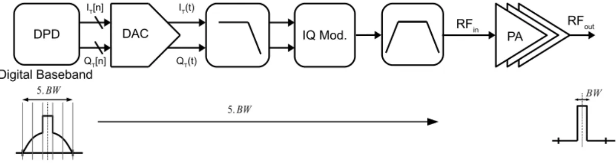
In DPD, the digital baseband modulated signal is subjected to the inverse nonlinear transfer characteristic of the power amplifier, in the digital baseband itself. Fig. 2.2
shows a transmitter chain employing a DPDsolution. To correct the inter-modulation distortion components of the PA, the spectrum regrowth occurs at the digital baseband itself, which is usually at least five times the input signal bandwidth.
In theDPD context, a proper behavioral model must be capable of characterizing the nonlinear distortion and memory effects. SincePDimplements the inverse function of
36 Chapter 2 State-of-the-Art Predistortion Techniques DPD QT[n] IT[n] DAC IT(t) QT(t) IQ Mod. PA Digital Baseband RFin RFout BW 5. BW 5. BW
Figure 2.2: Illustration of a BS transmitter employingDPDsystem
thePA,PD modeling is also a major part of the implementation. This section presents an overview of various existing memory-unaware and memory-aware DPD techniques available in the literature in a chronological way, later discussing the advantages and disadvantages of it. Note that ≤5 MHz input signal BW systems are considered as narrowband systems here. Also, unless stated otherwise the techniques are mainly applied for theBS HPA.
2.3.1 Memory-Unaware DPD
Memory-unaware models can only correct static nonlinearities of the PA and not the dynamic nonlinearities or memory effects of the PA and are mainly used in narrow-band predistortion. They are either Memory Less Look-Up Table (ML-LUT) based implementations or polynomial models based. ML-LUTimplementations dominate the memory-unaware predistortion scenario. Firstly, BS memory-unaware DPD methods are presented and later UE PA memory-unaware DPD methods are briefly discussed in this section.
One of the earliest examples is as shown in [66], adaptive predistortion for a Traveling Wave Tube (TWT)PAbased transmitter was implemented for 64 Quadrature Amplitude Modulation (QAM). The implemented system has predistorted values of in-phase and quadrature component voltages of each of the 64QAM constellation symbols in a RAM. A memory-lookup encoder obtains each input data symbol and generates the RAM addresses of the desired signal point. The corresponding stored, predistorted baseband voltage values are used. This method is custom tailored to 64 QAM and has to be completely redesigned to address other modulation formats. So this method is not suitable for the current multi-mode communication systems, where different kinds of modulation formats are employed based on different requirements.
Gain based Look-Up Table (LUT) method in [2], unrestricted to modulation format, exploits the fact that the memoryless nonlinearity of thePAonly depends on the envelope power of the input signal. As shown in Fig. 2.3, the envelope power |x(t)|2 of the input
Chapter 2 State-of-the-Art Predistortion Techniques 37
signal x(t) is quantized and used as the indexing parameter of the LUT. The readLUT
entry value is used to generate the predistorted signal z(t) by modifying the input signal to obtain a linear output y(t) at the PA.
PA
| . |2 LUTLUT
x[n] z[n] y(t)
Figure 2.3: Gain based LUT DPDof [2]
Among various power series models polynomial model is one of the most popular model for a quasi-memoryless nonlinearPA correction. The predistorter output zP D,P ol[n] is
given by: zP D,P ol[n] = x[n] K X k=1 ak|x[n]|k−1, (2.1)
where x[n] is the input signal, ak are the coefficients of the polynomial, K is the
nonlinearity order of the predistorter.
In the case ofUE PAs the memory effects are less pronounced [61] and hence memoryless models can suffice the PA modeling as well as predistortion, which is predominantly modeling nonlinearity [47]. Mostly this is accomplished by using simple ML-LUT. There are two schools of thoughts contradicting each other, to employ or not to employ adaptive predistortion for UE PAs. On one hand, Asbeck group claims [63] that the
DPD should be adaptive because the UE PA has large variations and mismatch in load when compared to BS DPDand is battery driven, which makes the PA distortion characteristics vary a lot. Also, in the context of Code Division Multiple Access (CDMA), the variation of the output power is in the excess of 70 dB which changes thePAlinearity characteristics for different power modes [63]. On the other hand, many authors have done PD implementation using a simpleML-LUTand recent publications have done it in a open-loop fashion claiming that in theUE applications, it is difficult to reconstruct the real-time DPDbecause of the sizes of additional circuits and their power consumption as detailed in [3,7].
In [63], a fast-real time adaptive DPDsystem (RT-ADPD) is shown and various issues associated with theUE PAare discussed. TheDPDis based onLUTs, one for amplitude and one for phase. The main differences are the usage of IF ADC, to avoid IQ imbalance coming from RF IQ modulator and converting the digitally down converted IQ data into polar form by using CORDIC (COordinate Rotation DIgital Computer) algorithm. Similarly, the quadrature Baseband (BB) signal is converted into polar form and is
38 Chapter 2 State-of-the-Art Predistortion Techniques
compared with the output after time alignment and theLUTs is adaptively adjusted. The adaptation takes less than 50 µs. It is implemented on an Field Programmable Gate Array (FPGA). The power consumption estimate of theFPGA implementation is not given as it is a prototype and has been mentioned that the optimized IC design realization will have very less power and the estimate is beyond the scope of the authors. It is also mentioned that usage ofDPD reduces thePA power consumption by around 350 mW and increases the Power Added Efficiency (PAE) by 10% [65]. The performance details are presented in the Table.2.1.
[3] presents a UE PA DPDwith a simpleML-LUTas shown in Fig.2.4, which consists of 128 entries, and it is extracted at the peak average output power level. The power level is scanned from 15 dBm to 31 dBm and a linear operation ofPA is assumed below the level. Control signal based on the average output power is used to index theML-LUT DPD, to address the large dynamic range in the UEPA scenario. The DPDimproves the Adjacent Channel Power Ratio (ACPR) from -29 dBc to -37 dBc, by 8 dB, at an average output power of 28 dBm over the entire range ofPAoperation, i.e., 1.7–2.0 GHz. The PA delivers a gain of 16–18 dB, with the PAEof 41.1–42%.
PA
LUT2nd
1st
128th
Increasing output power
Pout,avg
x[n] z[n] y(t)
Figure 2.4: LUT DPDindexed by average output control signal [3]
2.3.2 Memory-Aware DPD
This section presents memory-aware DPD methods, which are usually used in the context of BS HPA linearization. Similar to unaware DPD implementations, memory-aware DPDs also fall under LUT methods or models with nonlinear basis functions [67]. Volterra series proposed by Italian mathematician Vito Volterra in the year 1887 [68,69] can perfectly model nonlinearity as well as linear and non-linear memory effects of any non-linear system [61, 70, 67], which in our case is a DPD. It uses polynomial basis functions to describe nonlinearity and memory effects. The output signal of the Volterra
Chapter 2 State-of-the-Art Predistortion Techniques 39 series DPD is given by zP D[n]: zP D[n] = K X k=1 M X m1=0 · · · M X mk=0 ak(m1, ..., mk) k Y i=1 x[n − mi], (2.2)
where x[n] is the input signal, ak(m1, ..., mk) are the model coefficients, also called
Volterra kernels, K is the nonlinearity order and M is the memory depth of the predis-torter. The computational complexity of the model is very high for implementation of high memory order and nonlinearities and hence prohibitively high cost of computation and training in the context of linearization of small-cellBSs.
Hence less complex alternative implementations which are derivatives of Volterra series such as Memory Polynomials (MP) [71,42] are employed in most of the recent works [72,
73]. Memory polynomial model is a baseband model, derived from Volterra using narrowband approximation. Narrowband approximation assumes the signal bandwidth is small compared to that of the RF signal carrier frequency. Also, it doesn’t have the cross terms, when compared to Volterra series [43]. Cross terms refer to the product involving samples with different time shifts of their signal envelope samples. MP predistortion model’s output zP D,M P[n] is given by:
zP D,M P[n] = K X k=1 M X m=0 akmx[n − m]|x[n − m]|k−1 (2.3)
where x[n] is the input signal, akm are the model coefficients, K is the nonlinearity
order and M is the memory depth of the predistorter. The model is linear-in-parameters and its coefficients can be identified by indirect learning approach using least squares method [42] and can be made adaptive as well.
The MP simplification is effective but with expanding bandwidths, it has been found that the MP needs more Volterra cross terms to expand its capability. Generalized Memory Polynomial (GMP) is one such method where the delay terms adjacent to the diagonal in the matrix are also considered. The adjacent delay terms comes from the upper and lower diagonals and adds lagging and/or leading exponential envelope terms as explained in [43]. The output of GMP DPD is given by:
zP D,GM P[n] = Ka−1 X k=0 La−1 X l=0 aklx[n − l]|x[n − l]|k + Kb X k=0 Lb−1 X l=0 Mb X m=1 bklmx[n − l]|x[n − l − m]|k + Kc X k=0 Lc−1 X l=0 Mc X m=1 cklmx[n − l]|x[n − l + m]|k. (2.4)
40 Chapter 2 State-of-the-Art Predistortion Techniques
In the above equation, there are three polynomial components. The first polynomial is based on time-aligned input signal and its envelopes, which is memory polynomial term with the nonlinearity order Kaand the memory depth La. The second one is based on the
input signal and its lagging envelopes, with the nonlinearity order Kb and the memory
depth Lb and lagging envelope cross-term depth of Mb. The third polynomial component
is based on the input signal and its leading envelopes, with the nonlinearity order Kc and
the memory depth Lc and lagging envelope cross-term depth of Mc. The advantage of
GMP model is that it is still linear-in-parameters and indirect learning with least square estimation technique can be used to derive its coefficients. The disadvantage is that a large number of coefficients are required to see a noticeable linearization performance gain in comparison with MP DPD.
The paper [43] presents the effectiveness of the GMP for a 11-carrierCDMAinput signal with a total bandwidth of approximately 15 MHz. Digital-to-Analog Converter (DAC) and ADC evaluation boards were employed with a 30 W PA at 2.14 GHz. With a MP configuration, an ACLR of about 52.5 dB and up to 54 dB is achieved with 20 coefficients and 40 coefficients, respectively. With addition of cross terms further ACLR improvement is shown possible up to 58 dB as the tap coefficient number increases to 68. Similar simplifications of Volterra series has been recently presented in [74] known as Dynamic Deviation Reduction (DDR) by pruning the Volterra model in a systematic manner. Pruning is the process of keeping only the terms with noticeable impact and discarding other terms.
Other different methods exploit the Volterra series, like the memory fading Volterra series [70], which forces the memory depth to decrease with increasing kernel order. It has been found that the memory terms of higher order polynomial components of the Volterra series do not contribute as much as the lower order terms. Because of it, there is a 97% reduction in the terms when compared to a full Volterra model consisting of a 7th order kernel with memory depth 4. This is demonstrated in a very high power base-station LDMOS Doherty amplifier (350 W) for single and two-carrier WCDMA
signal.
![Figure 1.8: Illustration of effect of PAPR ; output power and efficeincy vs. input power [ 1 ]](https://thumb-eu.123doks.com/thumbv2/123doknet/2960434.81373/32.893.273.676.122.414/figure-illustration-effect-papr-output-power-efficeincy-input.webp)
![Figure 2.11: LUT based RF predistorter of [ 5 , 6 ]](https://thumb-eu.123doks.com/thumbv2/123doknet/2960434.81373/50.893.232.718.130.682/figure-lut-based-rf-predistorter.webp)
![Figure 2.14: Block diagram of the FIR-EMP ARFPD [ 9 , 10 ]](https://thumb-eu.123doks.com/thumbv2/123doknet/2960434.81373/53.893.113.731.377.601/figure-block-diagram-fir-emp-arfpd.webp)