O
pen
A
rchive
T
OULOUSE
A
rchive
O
uverte (
OATAO
)
OATAO is an open access repository that collects the work of Toulouse researchers and
makes it freely available over the web where possible.
This is an author-deposited version published in :
http://oatao.univ-toulouse.fr/
Eprints ID : 11413
To link to this article :
DOI:10.1109/TNS.2013.2286673
URL :
http://dx.doi.org/10.1109/TNS.2013.2286673
To cite this version :
Paillet, Philippe and Goiffon, Vincent and
Chabane, Aziouz and Girard, Sylvain and Rousseau, Adrien and
Darbon, Stéphane and Duhamel, Olivier and Raine, Mélanie and
Cervantes, Paola and Gaillardin, Marc and Bourgade, Jean-Luc and
Magnan, Pierre and Glebov, Vladimir Yu and Pien, Gregory
Hardening approach to use CMOS image sensors for fusion by
inertial confinement diagnostics. (2013) IEEE Transactions on
Nuclear Science, 60 (6). pp. 4349-4355. ISSN 0018-9499
Any correspondance concerning this service should be sent to the repository
administrator:
staff-oatao@listes-diff.inp-toulouse.fr
Hardening Approach to Use CMOS Image Sensors
for Fusion by Inertial Confinement Diagnostics
P. Paillet, Senior Member, IEEE, V. Goiffon, Member, IEEE, A. Chabane, S. Girard, Senior Member, IEEE,
A. Rousseau, S. Darbon, O. Duhamel, M. Raine, Member, IEEE, P. Cervantes, M. Gaillardin, Member, IEEE,
J. L. Bourgade, P. Magnan, V. Glebov, and G. Pien
Abstract—A hardening method is proposed to enable the use of CMOS image sensors for Fusion by Inertial Confinement Diagnos-tics. The mitigation technique improves their radiation tolerance using a reset mode implemented in the device. The results obtained evidence a reduction of more than 70% in the number of transient white pixels induced in the pixel array by the mixed neutron and
-ray pulsed radiation environment.
Index Terms—Active pixel sensor (APS), CMOS Image Sensor (CIS), dark current distribution, displacement damage dose (DDD), Geant4, inertial confinement fusion (ICF), neutrons, single-event transient (SET).
I. INTRODUCTION
M
EGAJOULE-CLASS laser facilities are devoted to the study of nuclear fusion by inertial confinement (ICF). Work is in progress both in the US (National Ignition Facility, NIF) [1] and in France (Laser Megajoule, LMJ) [2], and they will need plasma diagnostics to perform high neutron yield ex-periments. Such complex radiation environments can be found in existing facilities such as the Large Hadron Collider (LHC) [3], in other facilities currently being developed such as the In-ternational Thermonuclear Experimental Reactor (ITER) [4], and in future projects such as the High Power laser Energy Re-search (HiPER) [5] or the Laser Inertial Fusion Energy (LIFE) [6]. The different technologies usable for these diagnostics have been identified. Work is currently in progress to improve the tol-erance of the different subsystems’ response to the harsh radia-tion environments associated with such experiments [7], [8].Most of the existing diagnostics developed to image and ana-lyze the fusion plasma cannot withstand the high neutron yields associated with the future experiments, and one of the most sen-sitive parts of these diagnostics is the solid-state image sensor.
After a laser shot on a deuterium-tritium (D-T) target, the sensor needs to acquire an image of the X-ray emission asso-ciated with the fusion plasma. After generation, X-rays prop-agate from the target chamber center (TCC) inside the facility to finally interact with a Radiation to Light Converter (RLC), a long-persistence scintillator. This RLC converts the X-ray signal into another signal at visible wavelengths where it can be cap-tured by an appropriate high-performance silicon imager. Unfor-tunately, the radiation pulse contains not only the X-ray emission but also the 14 MeV neutrons from the D-T reaction. These neu-trons and their induced secondary particles also interact with the sensor and create a parasitic signal captured simultaneously with the useful visible signal. This dramatically impacts the image quality. It will affect the sensor performance for low-intensity shots. For more intense experiments, this transient perturbation will blind the sensor. In applications for which hardening by system solutions based on the difference of time travels of neu-trons and X-rays cannot be found, diagnostic designers will be forced to use more robust back-up diagnostic solutions (using solid state films for example), at the price of image quality.
The radiation response of complementary metal oxide semi-conductor (CMOS) image sensors (CIS), also called Active Pixel Sensors (APS), has been widely studied as these devices have been considered for use in radiation environments such as space [9]–[11], military applications or vision systems in nuclear industries [12]. Previous experiments have shown that CIS devices are good candidates for such imaging applications [13]–[16], this work will show that they can partially solve this long standing issue, by a system-level hardening approach combining the use of a long persistence scintillator and a specific mode of CIS operation.
The paper is organized as follows: the experimental details with the description of the test setup and facility are given in Section II. The raw experimental results are presented in Section III, most have been published as a short 2-page paper in IEEE Electronics Letter [16]. They are given here for clarity, limited to the amount needed for readers to understand this paper without having to constantly look back at the reference. The current manuscript is an extension of the Letter, providing additional experiments and discussions in Section IV, regarding the origin of the results observed experimentally.
II. EXPERIMENTALDETAILS
A. Tested Devices
A dedicated CIS has been designed and manufactured using a m CMOS process optimized for imaging application
Fig. 1. Synoptic diagram of the test setup in the LLE OMEGA facility.
(e.g., with optimized doping profiles, metal stack and optical in-terfaces, etc).. The tested CIS is made of pixels, each with three N-channel Metal Oxide Semiconductor Field Effect Transistors (MOSFETs) and one photodiode. It was designed by the Image Sensor Research Team of the Institut Supérieur de l’Aéronautique et de l’Espace (ISAE), Toulouse. The on-chip electronics have been deliberately restricted to the functions strictly necessary to operate the sensor in order to reduce the possible occurrence of Single Event Effects (SEE).
B. Test Setup
The experiment was conducted at the OMEGA laser facility of the Laboratory for Laser Energetics (LLE), University of Rochester, New York. A dedicated test bench was developed to simulate the timing sequence of operation of a plasma diag-nostic instrument.
An overview of the test bench is presented in Fig. 1. It is designed to acquire the images and to operate the sensor in different acquisition modes. The CIS itself, the Field Pro-grammable Gate Array (FPGA) required to drive the acquisition and the Analog-to-Digital-Converter (ADC) are all located in The Target Bay, as close as possible to the Target Chamber. The data acquisition board and computer are located in the instrumentation zone of the OMEGA Facility (called “La Cave”), where the radiation level is not significant.
The CIS is driven by a radiation tolerant ACTEL/Microsemi AX500 FPGA device, based on an antifuse technology, care-fully selected to ensure that no configuration loss can happen during or following each radiation pulse. Even though the se-lected 14-bit Analog-to-Digital-Converter (ADC) is not a radia-tion tolerant product, it exhibits a good tolerance to Single Event Latchup (SEL) and was not affected by the radiation levels of our experiment. The outputs of the ADC and the synchroniza-tion signals from the FPGA are connected to the computer by 30 m long optical fibers (Fig. 1). The conversion from the elec-trical output of the ADC to light into the optical fibers is per-formed using laser diodes, known and characterized to be im-mune to neutron induced degradation [20].
Fig. 2. Timing diagrams illustrating the standard CCD readout operation, the dump and read technique and the proposed CIS global reset technique.
Optical fibers were chosen because of their intrinsic immu-nity to the neutron pulse and the intense electromagnetic radia-tion pulse following the laser shot [17]. The basic idea is that it was designed to prevent (as much as possible) any loss of image acquisition due to SEE induced by the specific radiation envi-ronment. In addition to the use of optical fibers, electromagnetic issues were taken care of by placing all the electronics in a ded-icated shielded box.
Since the CIS test bench is located outside of the Target Chamber, a direct detection of the X-ray emission cannot be performed because it is blocked by the walls of the Target Chamber. Therefore the useful signal, the one that would have to be detected by the diagnostic instrument, needs to be simu-lated by a pulsed ultraviolet (UV) light emitting diode (LED), synchronized with the radiation pulse to excite a slow-decay RLC (persistence around a few ms), representative of a real signal. A test pattern was placed after the RLC to make sure that the sensor properly acquires the simulated useful signal.
C. Sensor Operation and Mitigation Technique
Current plasma diagnostics need solid-state image sensors, and mostly use charge-coupled devices (CCD). The standard timing diagram of CCD-based plasma diagnostic instruments is presented in Fig. 2. As already explained in the introduction sec-tion, at early times after a laser shot, the image of the x-ray pulse (the RLC signal) is perturbed by the neutron-induced parasitic charges in the pixels (stripped area in Fig. 2). In the classical CCD operating mode (CCD w/o dump), this parasitic signal is captured simultaneously with the useful visible signal.
The dump and read technique (CCD dump and read in Fig. 2) [7], [18] tries to overcome the problem by dumping the parasitic charges. In this case, a slow-decay RLC is required to delay the useful signal long enough to enable its acquisition in the frame immediately following the dump phase. An improvement of this mitigation approach, the fast dump and read technique, has been proposed for CCD, reducing the time required to remove the parasitic charges [19].
Here we propose a technique to adapt the CCD fast dump and read method to APS devices, using the so-called Global Reset (GR) mode. The main objective is to combine several advan-tages of CIS over CCD, such as a much higher intrinsic toler-ance to radiation and the possibility to use radiation hardening by design techniques to enhance their radiation tolerance, and to
investigate the possibility of further reducing the time required to evacuate the parasitic charges.
The GR mode available in the sensor consists of a syn-chronous reset of all the pixels at once, performing an instan-taneous fast dump and read operation, as illustrated in Fig. 2 (CIS Global Reset). The GR mode is activated before the laser shot (typically several milliseconds) to empty the pixel array of all dark charges. When the radiation pulse interacts with the imager, the generated parasitic charges are instantaneously evacuated from all pixels. The GR mode is then disabled after a varying delay (GR delay), kept as short as possible, to start the integration of the largest amount of useful signal still remaining. Clearly, reducing the GR delay will significantly improve the signal to noise ratio by increasing the number of useful signal charges.
D. Radiation Tests
The vulnerability of the image sensors has been evaluated during a high-yield deuterium-tritium fusion campaign at the OMEGA Laser facility (Laboratory for Laser Energetics, Uni-versity of Rochester) [8]. The average neutron yield induced by the laser shots was of about neutrons per shot, which roughly corresponds to an average fluence of n/cm at the location of the detector. 90% of the dose is generated during the first 370 ns of the experiment, and the dose rate, initially at a high level, drops rapidly to a negligible level [8]. The major threat to the device operation consists of neutron effects, since the TID at the device level is estimated below 5 mrad (SiO ) per shot.
To discriminate between the effects induced by the photons and neutrons, the facility called ELSA (CEA, France) was used. It is a linear accelerator which produces Brehmstrahlung gammas from a pulsed electron beam hitting a Tantalum target. The facility delivers s long pulses of 18 MeV gammas, with a recurrence from 0 (single shot) to 10 Hz.
III. EXPERIMENTALRESULTS
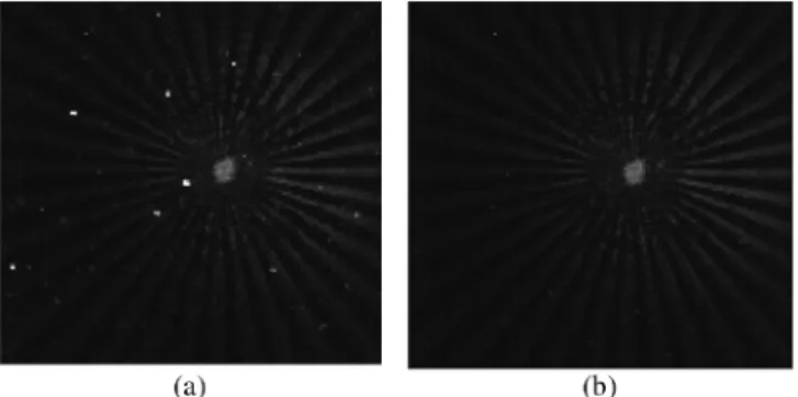
The test pattern used in combination with the UV-LED shows that the sensor properly acquires the simulated image, whether captured with the standard timing diagram (useful signal and parasitic signal acquired simultaneously) or with the GR fast dump technique. The respective images are presented in Fig. 3 for the same neutron yield. The test pattern is clearly visible in both operating modes, showing that the GR mode does not degrade the image quality [16]. It can also be noticed that the transient perturbations (parasitic white pixels) are almost com-pletely removed when the GR mode is activated.
A more precise estimation of the efficiency of the GR mode can be obtained if the test pattern is removed from the image. Before each laser shot, an image of the test pattern is captured in the absence of a radiation pulse, and recorded to serve as a reference. After each laser shot, this reference image (acquired immediately before the shot) is subtracted from the one just ac-quired. This subtraction of the test pattern is shown in Fig. 4. If no radiation-induced perturbations were present, the result of this operation should lead to an entirely black image. Obviously, the presence of any transient white pixel (i.e. a trace of
neu-Fig. 3. RLC and test pattern image captured during a laser shot, from [16]. (a) Image acquired with the standard timing diagram (no GR). (b) Image ac-quired with the GR fast dump technique.
Fig. 4. Dark image obtained after subtraction of the test pattern image to the images presented in Fig. 3, from [16]. (a) Image acquired with the standard timing diagram (no GR). (b) Image acquired using the GR fast dump technique.
tron-induced degradation) in this resulting image is particularly highlighted and easy to observe.
Fig. 4a shows the unambiguous presence of such parasitic charges when the sensor is operated in a classic CCD mode. On the contrary, Fig. 4b confirms that the GR mode dumps most of the radiation induced parasitic charges. Nevertheless, there are still some disturbed pixels remaining in the image taken with the GR mode. The delay after which the image acquisition started was set at s in the particular case of Fig. 4b.
In order to investigate the origin of these remaining charges, the GR delay has been varied to study the influence of this pa-rameter on the effectiveness of the charge dumping technique. Tuning the GR delay means changing the delay between the ra-diation pulse and the end of the GR phase (see Fig. 2), when the image acquisition is started. Fig. 5 represents the numbers of disturbed pixels expected with the different GR delays.
Each number corresponds to a given laser shot, thus the neu-tron yield varies for each case. In order to compare the num-bers, they were normalized to a neutron yield. The number of disturbed pixels measured when the sensor is operated as a classic CCD (i.e. when the GR mode is not used) is represented as a dashed line in Fig. 5, and will serve as a reference to eval-uate the effectiveness of the GR technique. Using a GR delay of s leads to a removal of more than 70% of the parasitic white pixels, showing that the proposed technique has a remarkable efficiency. Increasing the GR delay after the radiation pulse fur-ther decreases the number of white pixels, but the decay is seen to be surprisingly slow, much more than could be expected [16].
Fig. 5. Normalized number of parasitic white pixels as a function of GR delay. The value achieved with the classical timing diagram (i.e. without GR) is rep-resented by a dashed line, from [16].
IV. DISCUSSION
Two main possibilities could explain this slow decaying be-havior: first, the decay could be entirely artificial, due to an elec-tronic time constant originating from the sensor or its associated electronics; second, the slow decay could have a physical origin, such as a time constant due to the complexity of the radiation environment itself. These two hypotheses are investigated in the following sections.
A. Origin of the Slow Decay: An “Electronic” Time Constant?
In the first case, it would mean that the GR phase is too short to dump all the charges deposited by the instantaneous radiation pulse. Such a mechanism is not expected to induce such long de-lays. Even a full reset of the sensor when it is entirely saturated by a light pulse should take less than a few microseconds.
Nevertheless, in order to settle the issue, a dedicated set of ex-periments were performed using the pulsed 18 MeV -rays ma-chine ELSA. Photons are not subject to the same diffusion pro-cesses as neutrons, thus there cannot be any contribution from diffused particles reaching the sensitive volume at later times after the photon pulse.
The results are presented in Fig. 6, where the distribution of the number of charges generated by photon pulses is plotted versus GR delays. As a reference here again, we also plot the same distribution for a dark image, acquired when no radiation pulse is used (no transient white pixel in the CIS). Looking at Fig. 6, it is obvious that all distributions are superimposed, ex-cept for the one measured with “No GR” (i.e. when the image captures all of the parasitic charges). As soon as the GR dump phase is activated, even with a GR delay as short as 5 ns, the distribution of charges is identical to that of the initial dark image. Thus, no parasitic charge is detected after a photon-in-duced pulse, even for delays much shorter than the ones used at OMEGA. The slow decay observed in Fig. 5 cannot be at-tributed to a sensor time constant to dump the charges.
B. Origin of the Slow Decay: The Radiation Environment?
The second hypothesis would imply that the OMEGA mixed pulse is not as short as initially expected, and that some delayed particles do reach the sensor after the GR dump phase. High-energy neutrons are known to interact with all materials sur-rounding the target (instruments, walls of the experimental hall, etc…) through a multiple diffusion process. Some of these
dif-Fig. 6. Distribution of the number of charges generated by photon pulses at the ELSA facility, using the GR technique at different delays after the gamma pulse (5 ns, 10 ns, 1 ms).
fusing neutrons could reach and interact with the sensor several micro-seconds or even milliseconds after the radiation pulse.
The Geant4 code [23]–[25] was used to simulate the evolu-tion with time of the radiaevolu-tion environment at the locaevolu-tion of the sensor. This evolution with time can be calculated once the main features of the geometry of the Experiment Hall of OMEGA have been described with enough details to account for the dif-fusion process degrading the particle energy. This geometry is simulated using the Monte Carlo Geant4 simulation toolkit ver-sion 9.4. The 80 m long experimental hall is described with all the surrounding walls and pillars, as well as the 3 m-diameter Target Chamber (an aluminum sphere). The focus of the sim-ulation is on neutron and gamma fluences and their evolution with time after generation, therefore the G4NeutronHP physics list is used; and the charged particles generated are not taken into consideration to reduce calculation time. A total number of simulated 14 MeV neutrons are emitted isotropically from a point source located at the center of the target chamber. This number is a trade-off between good statistics and duration of the calculation (High Performance Computing resources were still required for this simulation [26]). The resulting environ-ment (particle, energy, hit time) is recorded with a perfect de-tector located outside the target chamber at a distance of 5 m from the Target Chamber Center (TCC), the one at which the APS sensor was positioned during the experiment.
During their interaction with materials present in the experi-mental hall, neutrons also generate other particles. Charged par-ticles are not considered here mostly because their range is too short to really have a significant contribution. Including them in the calculation would lead to a significant increase of the sim-ulation time. The generated gamma rays on the other hand can propagate and impact the APS sensor, therefore their contribu-tion is taken into account.
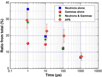
The first preliminary results of these calculations are shown in Fig. 7, as a function of time after the radiation pulse, together with the APS data from Fig. 5 for a direct comparison of the respective decay kinetics. The Geant4 calculations were per-formed by tracking neutrons (blue squares) and gammas (red circles), and the sum of their common contribution (green stars).
Fig. 7. Normalized number of parasitic white pixels in the APS as a function of GR delay (data from Fig. 5), compared to the calculated number of particles in the OMEGA environment, at the location of the device, at the corresponding times after the laser shot.
Two observations are obvious from Fig. 7. First, the decay mechanisms, both for neutrons and gammas, is similar to the one observed for white pixels in the APS. Second, the best fit to the APS data is obtained when both neutrons and gamma con-tributions are taken into account. This is especially true at early times ( s after the laser shot). It can be explained, since at early times most neutrons still have a high enough energy to generate a significant number of gammas, while at later times the diffusing neutrons lose more and more energy and gen-erate fewer gammas. The important point from Fig. 7 is that the Geant4 calculations show that delayed neutrons, induced by their interaction with the surroundings of the experiment, are actually present in the complex radiation environment, and in a ratio comparable to that of the experimentally observed tran-sient white pixels in the APS.
These first results show that the radiation environment can be calculated at the location of the tested CIS. Here we only focus on the evolution of neutrons and photons with time after their generation, in order to investigate if this evolution could explain the slow decay of transient white pixels observed experimen-tally. In the final application for LMJ, during the design phase of the experiment different locations are investigated for the di-agnostics. Each location will present a specific radiation envi-ronment, and codes like Tripoli [22] or Geant4 [23] are used to simulate these associated local environments. These simula-tions can be particularly useful to study the feasibility of a hard-ening-by-system study through shielding of the image sensor for example. It can also be used to predict both the permanent and transient degradations of an image sensor (not detailed here) at different positions. Additional calculations were performed and do confirm this hypothesis. It is indeed possible to model the degradations induced either by displacement damage dose or by ionizing events (such as Single Event Transients, SET) from any complex radiation environment. The details of these calcu-lations are beyond the scope of this paper, but they can be found in reference [27].
Fig. 8. Distribution of the number of charges generated by light pulses from a LED measured on the APS device at high level of saturation. The evolution of the distribution is investigated using the GR technique at different delays after the LED pulse (1 ns, 1 µs, 1 ms and 10 ms).
C. Limits of the Efficiency of the Hardening Technique
The experiments performed so far show that the GR tech-nique works remarkably well to reduce the number of transient parasitic charges collected by a CIS. The remaining work is to determine the limits of the technique. More specifically, one needs now to investigate what is the shortest GR delay required to ensure a complete dump of the parasitic charges. Our exper-iments so far have shown that a delay as short as 5 ns (Fig. 6 and associated discussion) is sufficient to remove all parasitic charges, when the radiation pulse is instantaneous. If this GR delay can be made even shorter, then the CIS will be able to cap-ture more signal from the decaying RLC scintillator. Also, Fig. 6 shows that the charge generated by photon pulses of moderate intensity can be efficiently removed by the GR dump phase, but we still need to investigate if this efficiency is as good for pixels with a higher level of saturation.
We therefore performed additional experiments to account for these remaining questions. The aim this time was to achieve a higher level of saturation in the pixels, compared to the data in Fig. 6. For these experiments, a fast LED was used to generate short light pulses at saturation level on the APS sensor. The data are presented in Fig. 8, in a way directly comparable with that of Fig. 6.
Here again, with only photons impinging on the sensor, the generation of charge in the device will be strictly instantaneous, without any contribution from diffused particles reaching the sensitive volume at later times after the light pulse. The distri-butions of the number of charges generated by photon pulses at different GR delays (1 ns, s, 1 ms and 10 ms) are presented in Fig. 8. As a reference here again, we also plot the same dis-tribution for a dark image, acquired when no radiation pulse is used (no white pixel in the CIS). The distribution measured with “No GR” (i.e. when the acquisition captures all of the parasitic charges), shows that the amount of light provided by the LED pulse was high enough to saturate most of the pixels. The dis-tribution peaks around 15000 a.u, a much higher level than that of Fig. 6 ( a.u.). The same LED pulse is used for all the
GR delays, thus the saturation level of generated pixels is the same in every case. Looking at Fig. 8, it is obvious again that, except for the one with “no GR,” all the distributions are su-perimposed. As soon as the GR dump phase is activated, even with a GR delay as short as 1 ns, the distribution of charges is identical to that of the initial dark image. With the GR mode activated, no parasitic charge is detected after a photon-induced pulse, even for delays as short as 1 ns, much shorter than the ones used during experiments at OMEGA. This confirms the result (already shown in Fig. 6) that the slow decay observed in Fig. 5 cannot be attributed to a sensor time constant to dump the charges. It will also be true should the sensor be completely saturated by parasitic charges.
These results demonstrate the ability of the Global Reset mode to efficiently remove all the parasitic charges generated during the GR phase, even when the pixels reach a high level of saturation. Such a high level of saturation in the pixels could be reached, for example, when the neutron flux increases by several orders of magnitude. This could be the case when the device is located much closer to the Target Chamber Center (TCC), and/or for laser shots at a higher neutron yield (LMJ shots vs OMEGA). If the APS device is able to acquire images inside the Target Chamber, where the neutron fluxes are orders of magnitude higher than at the location of the experiments described here, it could be used to directly image the X-rays produced by the reaction. This would lead to simpler designs for future diagnostic instruments, or enable existing ones to withstand laser shots with higher neutron yields than currently planned.
Future experiments will help to determine the limits of the technique, especially regarding the shortest GR delay needed to ensure a complete evacuation of the parasitic charges. This parameter is crucial, since even when using a slow decaying scintillator (or RLC), at longer times the amount of light emitted by the scintillator decreases significantly. Therefore, once the light emission starts to decay, the sooner the image acquisition is started the better. Thus, the use of the shortest possible delay will lead to the best image quality by increasing the signal to noise ratio.
The last topic to be addressed is the change in APS response with cumulated displacement damage dose. It is well-known that permanent effects are induced in neutron irradiated imagers. It has been first observed in CCD [28], [29], and is due to the creation of electro-active bulk defects acting as Generation-Re-combination centers in the pixel depleted volume. These dis-placement damage induced defects enhance the dark current of the damaged pixel. In a raw dark frame, these defects appear as gray or white spots, even in the absence of radiation. When using solid state imagers in ICF environments, the accumula-tion of laser shots will induce the generaaccumula-tion parasitic white and gray pixels by the successive neutron radiation pulses [28], [29], [30]. Recently, it was shown that the neutron flux does not have any significant effect on the displacement damage induced dark current [33]. Therefore existing data on displacement damage effects obtained at low and moderate neutron fluxes can be used to extrapolate the degradation induced at the very high flux reached during an inertial confinement fusion experiment. Thus, using Srour’s universal damage factor [31], estimations of the
average dark current level (or of the dark current distribution) after a given number of laser shots could be obtained [27], [33]. This increase in average dark current, together with most of the so called “hot-pixels”, induced after successive laser shots, can simply be removed by subtracting to the current image an average dark frame (as done here for example in Fig. 4) [32]. This subtraction technique is quite efficient at low to moderate level of permanent degradation. However, when the dark signal increases to high values, the subtraction could induce a loss of dynamic range which cannot be recovered.
Since the possibility of such high dark current can be pre-dicted [27], [32], [33], several mitigation options can be chosen. First, the use of very small integration time will significantly re-duce the number of integrated dark electron. Clearly for such an ICF experiment, an integration time reduced to a few millisec-onds would be enough to integrate the useful signal. Second, an-other available option would be to cool down the sensor, since the dark current is known to drop exponentially with tempera-ture. These techniques will extend the lifetime of the sensors used in these harsh environments by reducing the impact of pixels with high dark current values.
V. CONCLUSION
We showed that the global reset function integrated in the CMOS image sensors is effective for a MegaJoule class laser radiation environment. The technique was tested and validated in a real inertial confinement fusion facility. About 70% of the parasitic charges are removed after a s global reset phase.
The origin of the remaining 30% of transient white pixels has been identified: it is most likely due to diffusing neutrons losing energy through multiple scattering processes, which ultimately interact with the sensor, long after the end of the charge dump phase. Geant4 simulation of the time-dependence of the harsh environments at the device location in the OMEGA target bay confirms the presence of such energetic particles several mil-liseconds after the laser shot.
Additional experiments were performed to address the ability of the global reset technique to efficiently evacuate parasitic charges even when the pixels are saturated. They have shown that the technique can dump these saturating charges instanta-neously as well.
The next step will be to perform similar kinds of measure-ments inside the Target Chamber of an ICF facility, in order to investigate the ability of the APS sensor, using the Global Reset technique, to acquire images at higher neutron fluxes. Closer to the point source of the radiation pulse, and with the additional shielding provided by the target chamber, the environment will be different, and the radiation background will need to be inves-tigated. It is likely that the neutron distribution will be closer to the original 14-MeV pulse, and that optimal shorter delays for the GR technique will provide an even better reduction of the number of transient white pixels.
This definitely presents the APS technology as an interesting candidate not only for these applications, but also for all those where the GR Mode can bring an advantage. In the perspective of the LMJ project, the set of results presented in this work is extremely promising. It opens the way to efficient and reliable image sensors for diagnostics purposes.
REFERENCES [1] NIF [Online]. Available: https://lasers.llnl.gov [2] LMJ [Online]. Available: http://www-lmj.cea.fr [3] LHC [Online]. Available: http://lhc.web.cern.ch [4] ITER [Online]. Available: http://www.iter.org [5] HiPER [Online]. Available: www.hiper-laser.org [6] LIFE [Online]. Available: https://life.llnl.gov
[7] J.-L. Bourgade, R. Marmoret, S. Darbon, R. Rosch, P. Troussel, B. Villette, V. Glebov, W. Shmayda, J. C. Gommé, Y. Le Tonqueze, F. Aubard, J. Baggio, S. Bazzoli, F. Bonneau, J. Y. Boutin, T. Caillaud, C. Chollet, P. Combis, L. Disdier, J. Gazave, S. Girard, D. Gontier, P. Jaanimagi, H. P. Jacquet, J. P. Jadaud, O. Landoas, J. Legendre, J. L. Leray, R. Maroni, D. D. Meyerhofer, J. L. Miquel, F. J. Marshall, I. Masclet-Gobin, G. Pien, J. Raimbourg, C. Reverdin, A. Richard, D. Rubins de Cervens, C. T. Sangster, J. P. Seaux, G. Soullie, C. Stoeckl, I. Throin, L. Videau, and C. Zuber, “Diagnostics hardening for harsh en-vironment in Laser Mégajoule,” Rev. Sci. Instrum., vol. 79, p. 10F301, 2008.
[8] V. Glebov et al., in ITER-LMJ-NIF Int. Workshop, Cadarache, France, Jun. 2007.
[9] G. R. Hopkinson, “Radiation effects in a CMOS active pixel sensor,”
IEEE Trans. Nucl. Sci., vol. 47, no. 6, pp. 2480–2484, Dec. 2000.
[10] J. Bogaerts, B. Dierickx, G. Meynants, and D. Uwaerts, “Total dose and displacement damage effects in a radiation hardened CMOS APS,”
IEEE Trans. Electron Devices, vol. 50, no. 1, pp. 84–90, Jan. 2003.
[11] V. Goiffon and P. Magnan, “Radiation damages in CMOS active pixel sensors,” presented at the Imaging Systems Applications, 2011, OSA Tech. Dig., paper IMA3.
[12] J.-M. Armani, P. Barrochin, F. Joffre, R. Gaillard, F. Saigné, and J. L. Mainguy, “Enhancement of the total dose tolerance of a commercial CMOS active pixel sensor by use of thermal annealing,” in Proc. Conf.
Radiation Effects On Components and System, 2011, pp. 340–344,
paper PD2.
[13] Y. Tanimura and T. lida, “Effects of DD and DT neutron irradiation on some Si devices for fusion diagnostics,” J. nuclear materials, vol. 258-263, pp. 1812–1816, 1998.
[14] J. Baggio, M. Martinez, C. D’hose, and O. Musseau, “Analysis of tran-sient effects induced by neutrons on a CCD image Sensor,” Proc. SPIE, vol. 4547, pp. 105–115, 2002.
[15] V. Goiffon, S. Girard, A. Chabane, P. Paillet, P. Magnan, P. Cer-vantes, P. Martin-Gonthier, J. Baggio, M. Estribeau, J.-L. Bourgade, S. Darbon, A. Rousseau, V. Yu, G. Glebov, Pien, and T. C. Sangster, “Vulnerability of CMOS image sensors in megajoule class laser harsh environment,” Opt. Exp., vol. 20, pp. 20028–20042, 2012.
[16] V. Goiffon, S. Girard, P. Paillet, P. Magnan, A. Chabane, A. Rousseau, S. Darbon, P. Cervantes, and J. L. Bourgade, “Mitigation technique for the use of CMOS image sensors in Megajoule class laser radiative environment,” IEE Electron. Lett., vol. 48, pp. 1338–1339, 2012. [17] S. Girard, J. Baggio, and J. Bisutti, “14-MeV neutron, gamma-ray, and
pulsed X-ray radiation-induced effects on multimode silica-based op-tical fibers,” IEEE Trans. Nucl. Sci., vol. 53, no. 6, pp. 3750–3757, Dec. 2006.
[18] G. J. Yates and B. T. Turko, “Circumvention of radiation-induced noise in CCD and CID imagers,” IEEE Trans. Nucl. Sci., vol. 36, no. 6, pp. 2214–2222, 1989.
[19] G. W. Smith, G. J. Yates, J. R. Howorth, P. A. Smith, C. L. Seymour, and J. D. Bell, “Imaging with gated micro-channel plate intensifier camera systems in radiation environments,” Proc. SPIE, vol. 3872, pp. 148–159, 1999.
[20] E. Pailharey, J. Baggio, C. D’hose, and O. Musseau, “Reliability of 1300 nm laser diode for space applications. In photonics for space and radiation environments,” in Proc. SPIE 1999, vol. 3872, pp. 139–147, Berghmans and Francis, Eds.
[21] J.-L. Bourgade, V. Allouche, J. Baggio, C. Bayer, F. Bonneau, C. Chollet, S. Darbon, L. Disdier, D. Gontier, M. Houry, H. P. Jacquet, J. P. Jadaud, J. L. Leray, I. Masclet-Gobin, J. P. Negre, J. Raimbourg, B. Villette, I. Bertron, J. M. Chevalier, J. M. Favier, J. Gazave, J. C. Gomme, F. Malaise, J. P. Seaux, V. Yu Glebov, P. Jaanimagi, C. Stoeckl, T. C. Sangster, G. Pien, R. A. Lerche, and E. R. Hodgson, “New constraints for plasma diagnostics development due to the harsh environment of MJ class lasers,” Rev. Sci. Instrum., vol. 75, pp. 4204–4212, 2004.
[22] H. P. Jacquet, L. Lachèvre, and M. Messaoudi, “Activation analysis and first occupational dose rates estimates for the laser megajoule fa-cility,” Radiat. Protection Dosimetry, vol. 116, pp. 290–292, 2005. [23] Geant4 [Online]. Available: http://geant4.web.cern.ch/geant4 [24] S. Agostinelli, J. Allison, K. Amako, J. Apostolakis, H. Araujo, P. Arce,
M. Asai, D. Axen, S. Banerjee, G. Barrand, F. Behner, L. Bellagamba, J. Boudreau, L. Broglia, A. Brunengo, H. Burkhardt, S. Chauvie, J. Chuma, R. Chytracek, G. Cooperman, G. Cosmo, P. Degtyarenko, A. Dell’Acqua, G. Depaola, D. Dietrich, R. Enami, A. Feliciello, C. Fer-guson, H. Fesefeldt, G. Folger, F. Foppiano, A. Forti, S. Garelli, S. Giani, R. Giannitrapani, D. Gibin, J. J. Gómez Cadenas, I. González, G. Gracia Abril, G. Greeniaus, W. Greiner, V. Grichine, A. Grossheim, S. Guatelli, P. Gumplinger, R. Hamatsu, K. Hashimoto, H. Hasui, A. Heikkinen, A. Howard, V. Ivanchenko, A. Johnson, F. W. Jones, J. Kallenbach, N. Kanaya, M. Kawabata, Y. Kawabata, M. Kawaguti, S. Kelner, P. Kent, A. Kimura, T. Kodama, R. Kokoulin, M. Kossov, H. Kurashige, E. Lamanna, T. Lampén, V. Lara, V. Lefebure, F. Lei, M. Liendl, W. Lockman, F. Longo, S. Magni, M. Maire, E. Medernach, K. Minamimoto, P. Mora de Freitas, Y. Morita, K. Murakami, M. Naga-matu, R. Nartallo, P. Nieminen, T. Nishimura, K. Ohtsubo, M. Oka-mura, S. O’Neal, Y. Oohata, K. Paech, J. Perl, A. Pfeiffer, M. G. Pia, F. Ranjard, A. Rybin, S. Sadilov, E. Di Salvo, G. Santin, T. Sasaki, N. Savvas, Y. Sawada, S. Scherer, S. Sei, V. Sirotenko, D. Smith, N. Starkov, H. Stoecker, J. Sulkimo, M. Takahata, S. Tanaka, E. Tcher-niaev, E. Safai Tehrani, M. Tropeano, P. Truscott, H. Uno, L. Urban, P. Urban, M. Verderi, A. Walkden, W. Wander, H. Weber, J. P. Wellisch, T. Wenaus, D. C. Williams, D. Wright, T. Yamada, H. Yoshida, and D. Zschiesche, “GEANT4-A simulation toolkit,” Nucl. Instrum. Meth.
Phys. Res. A, vol. 506, pp. 250–303, 2003.
[25] J. Allison, K. Amako, J. Apostolakis, H. Araujo, P. Arce Dubois, M. Asai, G. Barrand, R. Capra, S. Chauvie, R. Chytracek, G. A. P. Cirrone, G. Cooperman, G. Cosmo, G. Cuttone, G. G. Daquino, M. Donszel-mann, M. Dressel, G. Folger, F. Foppiano, J. Generowicz, V. Grichine, S. Guatelli, P. Gumplinger, A. Heikkinen, I. Hrivnacova, A. Howard, S. Incerti, V. Ivanchenko, T. Johnson, F. Jones, T. Koi, R. Kokoulin, M. Kossov, H. Kurashige, V. Lara, S. Larsson, F. Lei, O. Link, F. Longo, M. Maire, A. Mantero, B. Mascialino, I. McLaren, P. Mendez Lorenzo, K. Minamimoto, K. Murakami, P. Nieminen, L. Pandola, S. Parlati, L. Peralta, J. Perl, A. Pfeiffer, M. G. Pia, A. Ribon, P. Rodrigues, G. Russo, S. Sadilov, G. Santin, T. Sasaki, D. Smith, N. Starkov, S. Tanaka, E. Tcherniaev, B. Tomé, A. Trindade, P. Truscott, L. Urban, M. Verderi, A. Walkden, J. P. Wellisch, D. C. Williams, D. Wright, and H. Yoshida, “Geant4 developments and applications,” IEEE Trans. Nucl.
Sci., vol. 53, no. 1, pp. 270–278, Feb. 2006.
[26] High Performance Computing at CEA [Online]. Available: www-hpc. cea.fr/index-en.htm
[27] M. Raine, V. Goiffon, S. Girard, A. Rousseau, M. Gaillardin, P. Paillet, O. Duhamel, and C. Virmontois, “Modeling approach for the prediction of transient and permanent degradations of image sensors in complex radiation environments,” IEEE Trans. Nucl. Sci., to be published. [28] J. R. Srour, C. J. Marshall, and P. W. Marshall, “Review of
displace-ment damage effects in silicon devices,” IEEE Trans. Nucl. Sci., vol. 50, no. 6, pp. 653–670, Dec. 2003.
[29] J. Killiany, “Radiation effects on silicon charge-coupled devices,”
IEEE Trans. Compon., Hybrids, Manufact. Technol., vol. 1, pp.
353–365, 1978.
[30] A. M. Chugg, R. Jones, M. J. Moutrie, J. R. Armstrong, D. B. S. King, and N. Moreau, “Single particle dark current spikes induced in CCDs by high energy neutrons,” IEEE Trans. Nucl. Sci., vol. 50, no. 6, pp. 2011–2017, Dec. 2003.
[31] J. R. Srour and D. H. Lo, “Universal damage factor for radiation-in-duced dark current in silicon devices,” IEEE Trans. Nucl. Sci., vol. 47, no. 6, pp. 2451–2459, Dec. 2000.
[32] L. Scheick and L. Edmonds, “Measurement of device parameters using image recovery techniques in large-scale IC devices,” IEEE Trans.
Nucl. Sci., vol. 41, no. 6, pp. 3649–3657, Dec. 2004.
[33] C. Virmontois, V. Goiffon, P. Magnan, S. Girard, O. Saint-Pé, S. Petit, G. Rolland, and A. Bardoux, “Similarities between proton and neu-tron induced dark current distribution in CMOS image sensors,” IEEE
![Fig. 3. RLC and test pattern image captured during a laser shot, from [16].](https://thumb-eu.123doks.com/thumbv2/123doknet/3552994.104094/4.888.461.824.97.278/fig-rlc-test-pattern-image-captured-laser-shot.webp)