HAL Id: hal-02917592
https://hal.univ-grenoble-alpes.fr/hal-02917592
Submitted on 18 Nov 2020
HAL is a multi-disciplinary open access archive for the deposit and dissemination of sci-entific research documents, whether they are pub-lished or not. The documents may come from teaching and research institutions in France or abroad, or from public or private research centers.
L’archive ouverte pluridisciplinaire HAL, est destinée au dépôt et à la diffusion de documents scientifiques de niveau recherche, publiés ou non, émanant des établissements d’enseignement et de recherche français ou étrangers, des laboratoires publics ou privés.
Effect of the Plasma Etching on InAsP/InP Quantum
Well Structures Measured through Low Temperature
Micro-Photoluminescence and Cathodoluminescence
Jean-Pierre Landesman, Nebile Isik Goktas, Ray Lapierre, Shahram
Ghanad-Tavakoli, Erwine Pargon, Camille Petit-Etienne, Christophe
Levallois, Juan Jiménez, Shabnam Dadgostar
To cite this version:
Jean-Pierre Landesman, Nebile Isik Goktas, Ray Lapierre, Shahram Ghanad-Tavakoli, Erwine Pargon, et al.. Effect of the Plasma Etching on InAsP/InP Quantum Well Structures Measured through Low Temperature Micro-Photoluminescence and Cathodoluminescence. ECS Transactions, Electrochemi-cal Society, Inc., 2020, 97 (2), pp.43-55. �10.1149/09702.0043ecst�. �hal-02917592�
Effect of the Plasma Etching on InAsP/InP Quantum Well Structures Measured Through Low Temperature Micro-photoluminescence and Cathodoluminescence
J. P. Landesmana, N. Isik Goktasb, R. R. LaPierreb, S. Ghanad-Tavakolib, E. Pargonc,
C. Petit-Etiennec, C. Levalloisd, J. Jiméneze, and S. Dadgostare
a
Univ Rennes, CNRS, IPR - UMR 6251, 35000 Rennes, France
b
Department of Engineering Physics, McMaster University, Hamilton L8S 4L7, Canada
c
Université Grenoble Alpes, CNRS, LTM, 38000 Grenoble, France
d
Univ Rennes, INSA Rennes, CNRS, Institut FOTON—UMR 6082, 35000 Rennes, France
e
Dpto. Fisica de la Materia Condensada, Universidad de Valladolid, 47011 Valladolid, Spain
Photoluminescence and cathodoluminescence spectral imaging were performed across rectangular stripes etched in samples with InAsxP1-x quantum wells of constant thickness and variable
composition grown on InP. In particular, the effects of different etching chemistries (CH4/H2/Ar and Cl2/CH4/Ar) were investigated.
The results discussed deal with modifications of the luminescence line shapes (which differ with etching process) and with the intensity variation of the emissions associated with the quantum wells across the stripes. The possible origins of these effects are investigated in terms of carrier recombination on the vertical sidewalls of the stripes and lateral diffusion of species from the plasma during etching. Cathodoluminescence measurements on samples under DC-bias also show the quantum confined Stark effect which is correlated to the material modifications induced by the etching.
Introduction
Many fabrication processes for photonic devices in III-V semiconductors involve plasma etching, also designated as reactive ion etching (RIE), for the definition of features with anisotropic profile. For example, waveguides in InP-based materials with rectangular profiles are made using this kind of tool (1). However, plasma etching is also a possible source of defects in the material during the process. This issue has already been investigated by a number of groups. The induced disorder can be chemical, e.g. non-stoichiometry (2), crystallographic, e.g. creation of an amorphous layer or collision cascades (2, 3), and/or creating defects that affect the electronic and optical properties (4 – 6). Due to the preferential direction of ions impinging the material, horizontal etched surfaces and vertical sidewalls show different behaviors. Interaction mechanisms with the impinging ions and chemical radicals have been proposed to explain the disorder. Ion channeling and diffusion (5) in particular were suggested to explain disorder occurring at depths of hundreds of nanometers below the etched surface.
The details of the disordering effects still need to be understood, especially as new etching processes are being developed with enhanced performance (etch rate, selectivity, morphology, etc.).
We propose a study on the etching of InP using different etching processes. Our goal is to retrieve information about the effects on the optical properties of the etched features / devices through the use of luminescence-based techniques (photoluminescence - PL - and cathodoluminescence - CL). In particular, we exploit the potential for spatial resolution of these techniques (7). We use etched ridges with rectangular profiles and various widths. A specific objective is to discriminate between vertical effects (damage propagating perpendicular below the surface) and lateral affects (propagating parallel to the surface within the etched devices). In this aim, we have prepared samples with a series of quantum wells (QWs) at different depths below the surface. Each QW having its own identified optical signature allows in principle an analysis of the depth dependence of the disordering as was already shown (6). The spatial resolution of micro-PL (µPL) and CL yields information on the lateral effects. In addition to the changes in optical properties identified from modifications of the PL and CL spectra, we have also investigated the effects of an electrical DC bias and show that the quantum confined Stark effect (QCSE) can play a significant role in understanding the PL and CL spectra, and their changes upon etching (8).
Samples and Experiments
Sample Growth
QW samples were grown by gas source molecular beam epitaxy on InP (100) n-type substrates, using solid sources (In) and PH3 / AsH3 gases. First, an InP buffer is grown
(thickness: 300 to 400 nm). This buffer is followed by InAsxP1-x QWs with InP barriers.
The QW thickness is fixed for a given sample (typically 7 to 8 nm), while the As/P composition is changed from one QW to the following. The first QW on top of the buffer has the highest As content (typically in the order of x 0.5), while the QW closest to the surface has the lowest As content (x 0.35). In this growth sequence, QWs are separated by InP barriers of 100 nm and the structure is finally covered by a 300 nm layer of InP. Figure 1 shows a schematic of the QW samples (with 8 QWs; samples with 9 QWs were also used).
Figure 1. Epitaxial sample structure (sample grown with 8 QWs). InP (d = 300 nm) InP (d = 100 nm) InP (d = 100 nm) InP (d = 100 nm) InP (d = 100 nm) InP (d = 100 nm) InP (d = 100 nm) InP (d = 100 nm) Surface
InP buffer + substrate QW1
QW2
Decreasing the As content in the QWs from substrate / buffer to the surface increases the energy band-gap, ensuring that the PL or CL signal from deeper QWs will not be absorbed in the QWs above (see following sub-section).
Some samples were grown without any intentional doping, whereas other samples were grown with Be doping added to the InP buffer and barrier layers (p-type doping level 1018
cm-3).
Etching of Rectangular Ridges
Plasma enhanced chemical vapor deposition of silicon nitride SiNx was used as the
etching mask. This layer was grown at 250 °C with a thickness of 500 nm. Stripes of various widths (1 to 50 µm) were defined by optical lithography in this mask. After mask opening, the etching of the different samples was performed by plasma etching. Two different processes were used:
Process #1: capacitively coupled RIE reactor with CH4/H2/Ar gas mixture.
Process #2: inductively coupled RIE reactor with Cl2/CH4/Ar gas mixture.
The etch depth was 2 µm to ensure etching of all QWs.
Details for the Etching Process #1: After SiNx mask opening and resist stripping, the
InP etching was done with 6.4 sccm CH4 / 50 sccm H2 / 8.4 sccm Ar (total pressure:
30 mTorr), and a power of 40 W. No external sample heating was used.
After etching the InP, the polymer formed during the etching was first etched in the plasma using 50 sccm O2 (total pressure: 6 mTorr) with a power of 50 W, and the SiNx
mask was subsequently stripped in HF.
Details for the Etching Process #2: After SiNx mask opening and resist stripping, the
InP etching was done using 20 sccm Cl2 / 100 sccm Ar / 32 sccm CH4 (total pressure:
20 mTorr), a power of 800 W at the plasma source and 200 W for sample bias, and a sample temperature of 200 °C.
After etching the InP, the SiNx mask and polymer passivation were first etched in HF
and then stripped in the plasma using 90 sccm O2 (total pressure: 10 mTorr), and a power
of 800 W.
µPL Setup
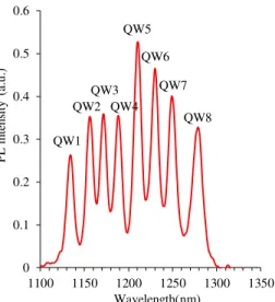
The µPL experiments were performed at 10 K using a specially designed optical cryostat (9). The chosen excitation wavelength was 1064 nm to avoid the generation of electron-hole pairs in the InP substrate, buffer and barrier layers. The excitation power density was approximately 5.107 W/cm2. The PL spectrum obtained under these conditions for an as-grown un-doped sample with 8 QWs, prior to etching, is shown in figure 2.
Figure 2. Low temperature (10 K) PL spectrum of an un-doped sample after growth (8 QWs). The lines are labeled with the QW number in the structure.
CL Setup
The CL spectral images were recorded in a Carl Zeiss (LEO 1530) field emission scanning electron microscope, equipped with a Gatan mono-CL2 system with a liquid nitrogen - cooled InGaAs array detector. These measurements were done on cooled samples (80 K). The acceleration voltage for the electron gun was set to 20 kV. The penetration depth for this voltage is in the order of 1 µ m (10). A typical CL spectrum obtained for an as-grown, un-doped sample can be seen in figure 3.
Figure 3. CL spectrum (80 K) of an un-doped sample after growth (9 QWs).
Experimental Results
As-grown Samples
We first comment on the spectra measured for the as-grown samples, before any etching process, such as shown in figs. 2 and 3. The signature of each QW can clearly be identified. The peaks are sharp (spectral width on the PL spectra at 10 K: 4.5 nm /
0 0.1 0.2 0.3 0.4 0.5 0.6 1100 1150 1200 1250 1300 1350 P L i n te n si ty (a .u .) Wavelength(nm) QW1 QW2 QW3 QW4 QW5 QW6 QW7 QW8 1150 1200 1250 1300 1350 1400 1450 CL i n te n si ty (a .u .) Wavelength (µm)
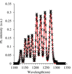
4.4 meV for the sharpest transition). These spectra display for each line a single, symmetric transition, indicating that a single hole level is apparently confined in the QWs due to compressive stress. A very good fit to the experimental PL spectra is obtained using Gaussian profiles for each line, with adjustable position, amplitude and width, as illustrated in figure 4.
Figure 4. Low temperature (10 K) PL spectrum. indicates measured data and red lines indicate the model fit.
Doping leads to a significant broadening of the emission lines (fig. 5).
Figure 5. Low temperature (10 K) PL spectrum of (a) un-doped sample; (b) doped sample. Both samples have the same epitaxial structure with 9 QWs, except for the Be-doping in the InP barriers in the case of the doped sample.
This broadening effect is most probably due to a transfer of the carriers in the InP barriers due to Be doping into the InAsxP1-x QWs. Because of this transfer, a range of
energy levels in the valence band becomes populated by holes. Under photo-pumping, the electrons created can recombine with holes in this entire range, thus broadening the PL signal (11).
CL spectra at 80 K yield similar trends as the PL spectra for the reference un-etched samples (8). 0 0.05 0.1 0.15 0.2 0.25 0.3 0.35 1100 1150 1200 1250 1300 1350 P L i n te n si ty (a .u .) Wavelength(nm) 1.08 1.18 1.28 1.38 P L i n te n si ty (a .u .) Wavelength (µm) 1.15 1.25 1.35 1.45 P L i n te n si ty (a .u .) Wavelength (µm) (a) (b)
PL Spectral Imaging on Etched Samples
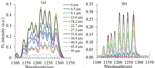
We now examine the spectral images produced by scanning the laser beam across etched stripes at 10 K in the µPL set-up. Raw data obtained for stripes (width: W = 50 µ m) etched using the different processes are displayed in figure 6.
The spectra in figure 6 were recorded on stripes etched from un-doped samples. The corresponding reference spectrum is shown in figure 2. Each spectrum was fitted with the model curve described above. Comparing with the reference spectrum, the following statements can be done:
- the CH4/H2/Ar process increases the spectral line width (average line width: 7 nm)
- the Cl2/CH4/Ar process slightly decreases the spectral line width (sharpest lines: 3.8
nm)
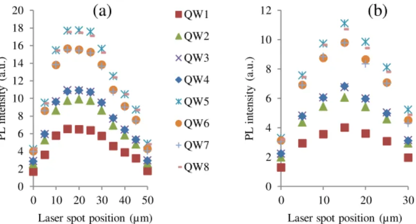
Fitting with the model curve also allows plotting the intensity variation for each line versus position of the laser beam across the stripes. Examples of intensity variations are shown in figure 7 for two different stripes (widths 30 and 50 µm respectively) etched with the CH4/H2/Ar process. The Cl2/CH4/Ar process gives similar trends for the intensity
distribution across the stripes. The main information derived from the intensity variation curves is the gradual decrease on both edges, extending over more than 10 µ m on each side. A plateau seems to be reached for the case of the 50 µm stripe, but not for the 30 µm stripe.
Figure 6. Series of µPL spectra measured at low temperature (10 K) across 50 µm ridges. (a) etching with CH4/H2/Ar, and (b) etching with Cl2/CH4/Ar. Each color corresponds to a
different position across the ridge as indicated by the legend in the center. The center of the ridge corresponds to the 25 µm position.
Figure 7. Integrated intensity for individual PL lines across stripes with etch depth 2 µm after the CH4/H2/Ar process. (a) Stripe width 50 µm, and (b) stripe width 30 µm.
CL Spectroscopy on DC-Biased Samples
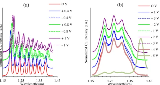
We focus here on the spectroscopic measurements performed in the CL set-up applying a DC bias on the surface of the sample, whereas the backside is grounded. Such measurements were performed only on the un-etched samples for the moment. Figure 8 illustrates the results for both an un-doped and a doped sample comprising 9 QWs. The surface voltage which could be applied varied from one sample to the other, depending on the magnitude of the generated current.
For both negative and positive applied voltage, the emission lines in the un-doped sample have a small red-shift. This red shift is due to the QCSE (12).
For the doped sample, no change is observed for voltages in the interval [- 4 V, +3 V] but as the voltage reaches – 5 V suddenly a strong emission dominates the spectrum. This emission is associated with QW 9, the closest QW to the InP buffer, i.e. in the zone where the p-n junction was created in the p-doped samples. With a negative bias on the surface of this sample a strong reverse situation is created, probably leading to a depletion of the minority carriers generated in the QWs closer to the surface.
0 2 4 6 8 10 12 14 16 18 20 0 10 20 30 40 50 P L i n te n si ty (a .u .)
Laser spot position (µm)
QW1 QW2 QW3 QW4 QW5 QW6 QW7 QW8 0 2 4 6 8 10 12 0 10 20 30 P L i n te n si ty (a .u .)
Laser spot position (µm)
Figure 8. CL spectra recorded at 80 K on samples DC-biased on the surface (9 QWs). (a) un-doped sample, and (b) doped sample. The spectra for different biases were vertically offset for clarity.
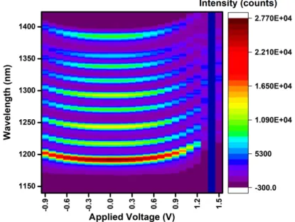
In order to better visualize the QCSE induced shifts of the QW lines for the un-doped sample, figures 9 and 10 give a 3-dimensional representation of the CL spectra under DC bias.
Figure 9. CL spectra measured at 80 K on the un-doped sample as a function of surface DC bias (- 0.9 to 1.5 V applied on the surface in steps of 0.1 V).
1.15 1.25 1.35 1.45 N o rm a li ze d CL i n te n si ty (a .u .) Wavelength(µ m) O V + 0.4 V - 0.4 V + 0.8 V - 0.8 V + 1 V - 1 V 1.15 1.25 1.35 1.45 N o rm a li ze d CL i n te n si ty (a .u .) Wavelength(µm) O V + 1 V + 3 V + 2 V - 1 V - 2 V - 3 V - 4 V - 5 V (a) (b)
Figure 10. Color map of the CL spectra shown in fig. 8.
Discussion
We first discuss the changes observed on the PL spectra upon etching with the different processes for the un-doped samples. Analyzing the results for the doped samples, however, was more difficult because of the line broadening.
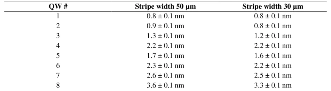
The spectral positions for the different QWs in etched stripes are shown in figure 11 (same sample as figure 7).
Figure 11. Spectral positions for individual PL lines across stripes with etch depth 2 µm after the CH4/H2/Ar process. The straight lines represent the corresponding positions on
the reference, un-etched, sample. (a) Stripe width 50 µm, and (b) stripe width 30 µ m.
Comparison with the line positions on the reference sample yields the red shifts as indicated in table I. 1120 1140 1160 1180 1200 1220 1240 1260 1280 0 10 20 30 40 50 W av el en g th (n m )
Laser spot position (µm)
1120 1140 1160 1180 1200 1220 1240 1260 1280 0 10 20 30 W a v el en g th (n m )
Laser spot position (µm)
TABLE I. Spectral shifts measured for the etched stripes (CH4/H2/Ar etching process).
QW # Stripe width 50 µm Stripe width 30 µm
1 0.8 ± 0.1 nm 0.8 ± 0.1 nm 2 0.9 ± 0.1 nm 0.8 ± 0.1 nm 3 1.3 ± 0.1 nm 1.2 ± 0.1 nm 4 2.2 ± 0.1 nm 2.2 ± 0.1 nm 5 1.7 ± 0.1 nm 1.6 ± 0.1 nm 6 2.3 ± 0.1 nm 2.2 ± 0.1 nm 7 2.6 ± 0.1 nm 2.5 ± 0.1 nm 8 3.6 ± 0.1 nm 3.3 ± 0.1 nm
There is a significant trend towards increasing red shift for QWs located deeper in the sample (with an exception for QW5). On the other hand, the spectral positions are remarkably constant across the stripes, contrary to line intensities (figure 7).
The line intensities show strong variations across the etched stripes. We tried fitting using a function with the form:
A (1 − Bexp −xL − Bexp x−WL ) [1] where A represents the PL signal which should be measured in an area not affected by the presence of the stripe edges, x the position along the stripe, W the stripe width, L the minority carrier diffusion length, and B a term that depends on the surface recombination velocity on the etched vertical walls (13, 14). More precisely, B has the form B = S
S+1
where S = v.τ
L . srv is the surface recombination velocity on the vertical etched walls,
the radiative lifetime, and S is called the reduced surface recombination velocity. The resulting fits are shown on figure 12 for a 30 µ m stripe etched with the CH4/H2/Ar
process (same sample as figure 7).
Figure 12. Curve fitting and experimental QW line intensities across a 30 µm stripe with etch depth 2 µ m after the CH4/H2/Ar process. The symbols have the same meaning as in
figure 7.
The parameters resulting from this fitting procedure are given in table II below.
0 2 4 6 8 10 12 0 10 20 30 P L i n te n si ty (a .u .)
TABLE II. Fitting parameters for PL line intensities measured on the 30 µm stripe (CH4/H2/Ar etching process). QW # A B S (reduced surface recombination velocity) L (µm) 1 13.3 0.72 2.57 22 2 8.4 0.72 2.57 10 3 10.7 0.73 2.7 11.8 4 18.5 0.73 2.7 19 5 24 0.76 3.17 15.8 6 22.5 0.74 2.85 16.7 7 18.9 0.74 2.85 14.3 8 20.5 0.75 3.0 14.1
The best fit curves agree reasonably well with the experimental data. Assuming the same diffusion length for all QWs, we get L = 15 ± 3 µm. This value indicates that the QWs have a very high quality and have not been degraded by the etching process. The reduced surface recombination velocity appears rather constant for all QWs (2.8 ± 0.2). Determination of the true surface recombination velocity requires measurement of the radiative life time.
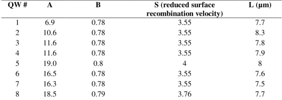
We applied the same fitting procedure for the 50 µm stripe of figure 7-a. Only the left half of the stripe was used for the fitting procedure as the right half shows some irregular behavior. The curve fitting is shown in figure 13, and the corresponding fitting parameters in table III. The diffusion length for this stripe is about half the diffusion length found for the 30 µm stripe, and the reduced surface recombination velocity is 30 % higher than found for the 30 µ m stripe. We do not really have an explanation for this, as both stripes were etched during the same process. However, the results show the interest of the measurement methodology based on the µPL set-up at low temperature for the evaluation of the impact of the plasma etching process on the material’s parameters.
Figure 13. Curve fitting and experimental QW line intensities across a 50 µm stripe (left edge) with etch depth 2 µ m after the CH4/H2/Ar process. The symbols have the same
meaning as in figure 7. 0 2 4 6 8 10 12 14 16 18 20 0 5 10 15 20 25 P L i n te n si ty (a .u .)
TABLE III. Fitting parameters for PL line intensities measured on the 50 µm stripe (CH4/H2/Ar etching process). QW # A B S (reduced surface recombination velocity) L (µm) 1 6.9 0.78 3.55 7.7 2 10.6 0.78 3.55 8.3 3 11.6 0.78 3.55 7.8 4 11.6 0.78 3.55 7.9 5 19.0 0.8 4 8 6 16.5 0.78 3.55 7.6 7 16.3 0.78 3.55 7.5 8 18.5 0.79 3.76 7.7
The bias-dependent CL spectra have shown that the QCSE can significantly affect the spectral positions and even line shapes in these samples. The next step will be to simulate this effect and evaluate if the penetration of some species from the etching plasma, for example ions formed either in the plasma phase or within the material as the stable form of these species, might affect the PL and CL spectra. This might, in particular, explain the changes in PL line shapes observed for the 2 different etching processes.
Conclusion
The µPL and CL spectroscopic measurements performed on InAsP/InP QW samples before and after plasma etching processes prove useful to evaluate the impact of the etching on some of the important parameters. These parameters are, in particular, the surface recombination velocity and the charge carrier diffusion length. Evaluating these parameters is important when fabricating such devices as photonic waveguides.
Acknowledgments
The authors would like to thank the Center for Emerging Device Technologies (CEDT) at McMaster University where epitaxial growth was performed. The authors also thank RENATECH+ (the French national network of facilities for micro-nano-technology) with NanoRennes and the LTM etching platform in Grenoble.
References
1. N. P. Siwak, X. Z. Fan, and R. Ghodssi, J. Micromech. Microeng., 25, 043001 (2015).
2. T. R. Hayes, U. K. Chakrabarti, F. A. Baiocchi, A. B. Emerson, H. S. Luftman, and W. C. Dautremont‐Smith, J. Appl. Phys., 68(2),785 (1990).
3. J. Etrillard, F. Héliot, P. Ossart, M. Juhel, G. Patriarche, P. Carcenac, C. Vieu, M. Puech, and P. Maquin, J. Vac. Sci. Technol. A, 14(3), 1056 (1996).
4. M. Rahman, J. Appl. Phys., 82(5), 2215 (1997).
5. D. L. Green, E. L. Hu, P. M. Petroff, V. Liberman, M. Nooney, and R. Martin, J.
Vac. Sci. Technol. B, 11, 2249 (1993).
7. M. Fouchier, M. Fahed, E. Pargon, N. Rochat, J. P. Landesman, D. Rouchon, J. Rocque, K. Rovayaz, E. Martinez, and S. Labau, MRS Adv., 3,57 (2018).
8. J. P. Landesman, J. Jiménez, C. Levallois, F. Pommereau, C. Frigeri, A. Torres, Y. Léger, A. Beck, and A. Rhallabi, J. Vac. Sci. Technol. A, 34(4), 041304 (2016). 9. C. M. Haapamaki, PhD Dissertation, McMaster University (2012).
10. J. Bonard, J. Ganière, B. Akamatsu, D. Araújo, and F. Reinhart, J. Appl. Phys.,
79(11), 8693 (1996).
11. D. F. Welch, G. W. Wicks, and L. F. Eastman, Appl. Phys. Lett., 46(10), 991 (1985).
12. L. Vina, E. E. Mendez, W. I. Wang, L. L. Chang, and L. Esaki, J. Phys. C Solid
State Phys., 20(18), 2803 (1987).
13. B. G. Mendis and L. Bowen, J. Phys. Conf. Ser., 326 (2011). 14. W. Van Roosbroeck, J. Appl. Phys., 26(4), 380 (1955).