Science Arts & Métiers (SAM)
is an open access repository that collects the work of Arts et Métiers Institute of Technology researchers and makes it freely available over the web where possible.
This is an author-deposited version published in: https://sam.ensam.eu
Handle ID: .http://hdl.handle.net/10985/6749
To cite this version :
Paul SANDULESCU, Lahoucine IDKHAJINE, Sébastien CENSE, Frédéric COLAS, Xavier
KESTELYN, Eric SEMAIL, Antoine BRUYERE - FPGA Implementation of a General Space Vector Approach on a 6-Leg Voltage Source Inverter - In: IECON 2011 - 37th Annual Conference on IEEE Industrial Electronics Society, Afghanistan, 2011-11-07 - IECON 2011 - 37th Annual Conference on IEEE Industrial Electronics Society - 2011
Any correspondence concerning this service should be sent to the repository Administrator : [email protected]
FPGA Implementation of a General Space Vector
Approach on a 6-Leg Voltage Source Inverter
P. Sandulescu1, L. Idkhajine1, S. Cense2, F. Colas1, X. Kestelyn1, E. Semail1, A. Bruyere3
1 L2EP, Arts et Métiers Paristech, 8 Bd Louis XIV, Lille France 2 Opal-RT Technologies Inc, 1751 rue Richardson Local 2525, Montreal, Canada 3 Valeo Powertrain Systems, 14 av. des Béguines, 95800 Cergy Saint-Christophe, France
Email: [email protected] Abstract – A general algorithm of a Space Vector
approach is implemented on a 6-leg VSI controlling a PM synchronous machine with three independent phases. In this last case, the necessity of controlling the zero-sequence current motivates the choice of a special family of vectors, different of this one used in Pulse Width Modulation (PWM) intersective strategy and in common Space Vector PWM (SVPWM). To preserve the parallelism of the algorithm and fulfill the execution time constraints, the implementation is made on a Field Programmable Gate Array (FPGA). Comparisons with more classical 2-level and 3-level PWM are provided.
Keywords – FPGA, Modulation strategies, Space vector,
Multiphase machine, Multiphase, Multi-leg. I-INTRODUCTION
When a VSI is controlled with a carrier-based PWM, the conduction durations of the switches have to be calculated to obtain the correct average values of the voltages applied to the load. The more classical way is the Suboscillation Method [1] which determines the intersections between a triangular shape wave and the desired average values of voltages. For a 3-leg 2-level VSI supplying a star connected load with isolated neutral, another method, more favorable to optimization [2], [3] is the SVPWM. Then, projections of the desired vectors must be achieved in order to obtain the conduction durations. However, this last method can hardly be generalized to the study of n-leg VSI supplying n-wire loads or even a 3-leg VSI supplying a star-connected load with neutral not isolated. It is always possible to use the Suboscillation Method but in this case, we no longer have the geometrical tools to analyze and optimize the performances of different control laws. A few works [4] were developed for 4-leg VSI implying a 3-dimensional approach using vectors that belong to a 3-dimensional space. Other works [5]-[7] use more general matricial methods for n-leg VSI but with no geometrical approach. Other works [8]-[9] split the problem into several 2-dimensionnal problems using properties of the load of the n-leg VSI. It is then possible to use space vector calculation developed for 3-leg VSI. However, there is a coupling between the planes since it is the projections of the same vectors which are used. Even if each vector reference in each plane can be obtained, it is still necessary to verify that the sum of these two references does not imply the saturation [10]-[11] of the n-leg VSI.
In order to propose a direct approach in n-dimensional space, a general geometrical vectorial characterization of VSI has been developed [12]-[14]. Then, the conduction durations, which can be considered as barycentric coordinates of a defined family of vectors, are calculated. The explicit calculations allow to find directly when saturation can occur and then to manage it [15]. The proposed general method can suffer from a high number of operations ((n+1) multiplications and (n-1) additions are necessary for the calculation of one time duration). In FPGA implementation these operations can be achieved in parallel treatment. On the contrary, in DSP implementation, the treatment is sequential. As consequence, to implement such an intensive treatment and at the same time ensure a high computational rate, the use of FPGA is suitable [16]-[18].
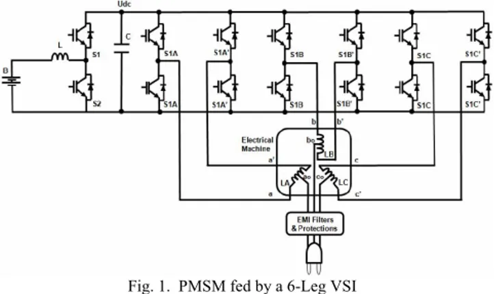
In this paper, a 3-phase Permanent Magnet Synchronous Machine (PMSM) with each phase being supplied by a 2-leg VSI is considered (Fig. 1). This configuration is studied for Traction drive of Electric Vehicle [19]-[23]. It is thus possible to use the same traction drive components as battery charger without need of any contactor. However, the use of three independent phases topology needs to take into account the zero-sequence current control, which is naturally equal to zero with classical star-coupled 3-phase machines. Imposed by the topology and necessary for the control strategy, a 6-leg VSI offers much more combinations (26=64) than the 8 combinations of 3-leg VSI. These 64 VSI states ensure many degrees of freedom to be managed by the voltage modulation strategy.
Fig. 1. PMSM fed by a 6-Leg VSI
The first section of this paper deals with the adaptation of the general space vector approach to the case of a 6-leg VSI supplying a PM synchronous machine with three
independent phases. A special Z-SVPWM (Zero Sequence Space Vector PWM) is proposed.
In the second section, the FPGA implementation is detailed.
In the third section experimental results are compared with those obtained with more classical 2-level and 3-level PWM.
II-CALCULATION OF TIME DURATION WITH Z-SVPWM
FAMILIES BY SPACE VECTOR APPROACH
A. Characterization of 6-leg VSI
The 6-leg inverter, represented in Fig. 2, imposes 3 voltages Vck. So, we associate to this converter a vectorial space E3 with an orthonormal basis of vectors
3 2 1, c , c c x x x .
We can then define the voltage vector as,
VcVc1xc1Vc2xc2Vc3xc3 (1)
Fig. 2. Topology of a 6-Leg VSI
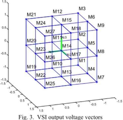
For each value of voltage, 3 combinations with values +E, 0 and –E are possible. Thus a family Fk of k=33=27 different voltage vectors vck characterizes the 6-leg VSI
and the 3 phase load.
A number k and a point Mk are associated with each possible vector vck . The vectors are represented varying
from M1 to M27, and form the vertices of a polyhedron B, which in our case is a cube as shown in Fig. 3.
Fig. 3. VSI output voltage vectors
B. Average control and barycenter notion
We consider a PWM with a period carrier T. The mathematical basis of this approach is to achieve average voltage by modulation of the pulse width. At the kT instant
Vc , the desired mean value of the instantaneous vector
) (t
Vc
can be expressed as follows,
1 0 ) 1 ( () 1 ) ( P r r r kT T k T t dt t T kT c cr c v v v
1 0 P r r r T t OM OM r (2)In this expression, tr is the activation duration of the
vector vcr . Since
1 0 P r r r t T , we have 1 1 0
P r r r T t (3)Consequently, the point M, defined as OM vc (kT), can be considered as the barycenter of the P points Mr,with the barycentric coordinates tr/T. The determination of time
duration is thus equivalent to the determination of barycentric coordinates.
Moreover, as tr is positive, M is inside the cube B as
shown in Fig. 5. So, when an average control is adopted, it is the entire volume of the cube B that characterizes the inverter, and not only its vertices.
C. How to find the switching durations
The determination of the barycentric coordinates is obtained in a n-dimensional space by calculation of determinants. The formulation is thus classical. In fact, the major problem is to choose interesting vectors among the 27 possible ones. There are a lot of possible solutions. It is then necessary to add a criterion in order to define a solution. In classical 2-level SVPWM, the nearest points of the desired point in the hexagon are chosen. This choice leads to a minimization of the high frequency current ripples. In the studied case, it is necessary to take into account that a zero-sequence current can be generated.
If the desired point is inside a plane, three non-aligned points in this plane are sufficient and a unique solution can be then obtained. In the studied case, it can be noticed that a family of seven points (M0, M6, M8, M16, M22, M20, M12), which have no zero-sequence component, belong to a plane (see Fig. 4). For each point M inside the hexagon HX generated by the seven points, it will be possible to generate adequate durations using only 3 points of this family with warrant of a strict instantaneous zero-sequence component value.
Fig. 4. 7-point family with no zero-sequence component
-1.5 -1 -0.5 0 0.5 1 1.5 -1.5 -1 -0.5 0 0.5 1 1.5 -1.5 -1 -0.5 0 0.5 1 1.5 M7 M8 M9 M4 M5 M6 M1 M2 M3 M16 M17 M18 Xc2 M13 M14 M15 Xc3 M10 M11 M12 Xc1 M25 M26 M27 M22 M23 M24 M19 M20 M21 -2 -1 0 1 2 -2 -1.5 -1 -0.5 0 0.5 1 1.5 2 M22 M16 M8 M6 M12 M20 M0 Hx
In this case, the maximum RMS value voltage in case of sinusoidal reference is limited to E
2 1 .
When looking at Fig. 5, it appears that a wider hexagon
Hy can be considered (Mp3, Mp21, Mp19, Mp25, Mp7, Mp9). In this case, these points are projections in the plane of the points which belong to the characteristic family F27 of the
6-leg VSI. As example Mp3 is the projection of M3. If minimum activation duration of switches is neglected, it is thus possible to obtain a wider hexagon Hy to which the
desired vector can belong. In this case, the maximum RMS value voltage in case of three sinusoidal references is limited to E
3
2 (15% greater than previously).
Fig. 5. VSI output 27-point family
For each new reference of the voltage vector, a search of the most accessible three nearest points of the hexagon is done by testing the sign of three scalar vector products. After determination of these three points, three determinants are calculated in order to obtain the time durations.
From the relations (2) and (3), tk, tj and tq, respectively
the time durations of the activation of the vectors
j
k OM
OM , and OMqare given by [14]:
j q k
q j k OM OM OM OM OM OM t | | det | | det
j q k
q k j OM OM OM OM OM OM t | | det | | det
j q k
j h q OM OM OM OM OM OM t | | det | | det III-FPGA IMPLEMENTATION OF THE ALGORITHM
In order to preserve the efficiency of the proposed space vector approach, the digital implementation is to be based on a fast digital target. Indeed, the time delay between the generation of the voltage references and the calculation of
the switching durations must be as small as possible. To this purpose, a hardware-based FPGA target has been chosen. Based on this hardware approach, the designer can develop an FPGA architecture that is perfectly dedicated to the algorithm. The parallelism of this algorithm is then preserved and consequently, the execution time is significantly shortened.
In the proposed application, the developed FPGA-based SVPWM has been implemented using the RT-LAB real-time platform (from OPAL-RT). The latter consists of, among others, a dual/quad core CPU board, a Xilinx Spartan3 FPGA board and a set of digital and analog I/O boards. In the following, we are going to present the structure of the control system, the FPGA architecture of the developed space vector module and finally the corresponding time/area performances.
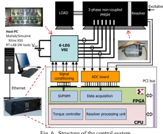
A. Description of the control system
The structure of the developed control system is shown in Fig. 6. The power stage consists of a 10-pole, 3-phase non-coupled, 0.9 kW, 1100 rpm, 8 Nm PMSM linked to a load and a Resolver position sensor. The stator is fed by the 6-Leg VSI. The digital control unit is composed of the RT-LAB platform. This platform includes a FPGA board and a CPU board that communicates through a PCI bus. The design of the whole controller is made using the dedicated Matlab/Simulink toolboxes (RT-LAB toolbox and Xilinx System Generator toolbox). The CPU implements the Torque controller (torque reference, PI-regulators, axes transformations) and the Resolver processing unit (extraction of the rotor position from Resolver signals). The proposed SVPWM module and the data acquisition module are implemented in the FPGA. The platform includes also a signal conditioning board (for the adaptation of the switching signals voltage level) and an ADC board (for the conversion of the stator currents and the Resolver signals).
Fig. 6. Structure of the control system
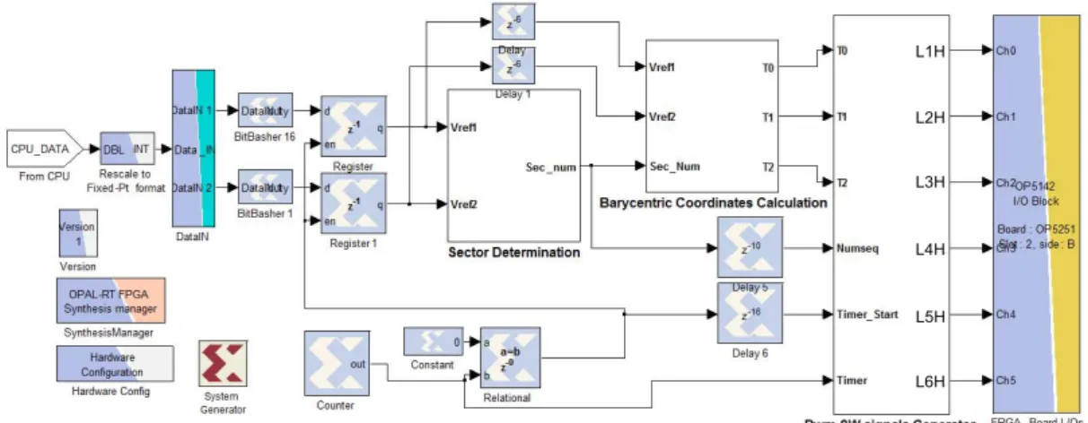
B. FPGA-based SVPWM module
The architecture of the implemented FPGA-based SVPWM is highlighted in Fig. 7. This architecture has been partitioned according to the algorithm presented previously. Roughly speaking, three main steps are processed: the sector determination, the barycentric coordinates calculation and
3-phase non-coupled PMSM Resolver LOAD PCI bus Host-PC Matlab/Simulink Xilinx XSG
RT-LAB SW tools 6-LEG VSI Excitation VDC FPGA CPU Ethernet SVPWM Data acquisition Torque controller ADC board Signal conditioning
Resolver processing unit
Hy
(4)
(5)
(6)
the switching signal generation. This design has been developed using the XSG toolboxes. Also, specific RT-LAB blocks have been included so as to manage the data transfer from the CPU and the interfacing with the FPGA I/O blocks.
C. Time/Area performances
The used FPGA target is a Xilinx XC3S5000 Spartan3 FPGA. The global clock frequency is equal to 100MHz. The latency (number of execution clock cycles) of the developed
SVPWM module is equal to 22. The execution time is then equal to 220ns which corresponds to a 0.088% time ratio. Note that the reference time in our case is the switching period that has been set to 250µs. As far as the FPGA resources consumption, the design occupies 8% of the 33280 FPGA cells and uses 14 hardwired 18-bit multipliers (over 104 multipliers). This is worth noticing that this consumption is directly linked to the format of the processed variables. In our case, the fixed point format has been set to 16Q10 (16 bits with 10-bit precision).
Fig. 7. FPGA-based SVPWM module
IV-SIMULATION AND EXPERIMENTAL VALIDATION
In this section, the principle of the 2-level PWM and the used 3-level PWM control is reminded. The Z-SVPWM will also be briefly explained. Afterwards the result of the Matlab/Simulink simulations will be presented. Finally, a comparison with the experimental results will be provided, highlighting the advantages and limitations of the proposed space vector method over the classical methods.
A. 2-level and 3-level pulse width modulation
Because of the need to control the zero-sequence current of the PMSM, the voltage vectors generated by the inverter will be analyzed. An efficient form of analysis is to project these vectors on to an electro-magnetically decoupled space. This is done using the Concordia transformation. The Concordia transformation projects the natural “abc” vectors to two separate space domains, one two dimensional plane, also called the “αβ” plane and a one dimension line, known as the zero sequence line. The electrical machine will also be viewed through the same perspective. Therefore the electrical machine is interpreted as two fictitious machines, each one being supplied by its own decoupled energy source (see Fig. 8).
In the case of a 2-level common modulation, for the given phase coupling of the electrical machine, the inverter will be able to generate a number of 8 vectors – combinations of –E;+E. These 8 vectors on the “abc” frame will generate the vertices of a cube as shown in Fig.3. The projections of the vertices of the cube on the Concordia frame generate the 6 vectors in the “αβ” plane and a suit of vectors on the zero sequence line with a non-zero value [13].
In the case of a 3-level modulation, taking into account the coupling of the electrical machine with the inverter, with respect to the 8 vectors generated with 2-level modulation, the inverter is also able to generate other 19 vectors – combinations of –E; 0; +E. In this case, a number of 7 vectors out of the total of 27 have zero sequence projection equal to zero, and moreover, these vectors are directly reachable in the “abc” frame as well, as shown in Fig. 5. A particular space vector modulation (called Z-SVPWM) can be defined, based on the use of these 7 vectors.
During a 2-level PWM time period, it is known that the intersection of the carrier with the reference value of the desired vector will generate at least two vectors (+E,+E,+E) and (-E,-E,-E) with the maximum amount 3E of zero sequence component. With respect to the time constant of the zero sequence fictitious machine, this increases the zero sequence current ripple.
Looking at the 3-level modulation, as shown in Fig. 5, it is perceptible that, during a PWM time period, there will always be two vectors that have a projection on the zero sequence line domain. Nevertheless, the vectors with zero sequence component only reach one third of the maximal amount over the 2-level method and are activated a fraction of the time with respect to the 2-level modulation. Therefore, it is expected to obtain a sensible reduction of oscillation on the zero sequence current component.
The Z-SVPWM uses vectors with no zero sequence component, therefore, in the case of a sinusoidal back e.m.f., we expect to have no zero sequence current flowing through the machine. L1H L2H L3H L4H L5H L6H
B. Simulation results of PWM strategies
A model of a PMSM with three independent phases was developed using Matlab/Simulink. The model is taking into account two fictitious machines, the zero sequence machine –M0 and the main machine – M1 as shown in Fig. 8.
Fig. 8. Graphical representation of the PMSM simulation model
For the simulation example it was decided to take the case of a perfect repartition of m.m.f and an equal time constant for the two fictitious machines. Having this in mind, it is expected to have good results applying the 3-level PWM strategy and a perfect result applying the space vector approach. In the case of the 3-level strategy, two types of modulation were implemented for the simulation and later on for the experimental results. The double modulation (DM) 3-level PWM [25] is expected to have better results over the simple modulation (SM) as the windings of the electrical machine are being supplied by the VSI at twice the value of the switching frequency.
Fig. 9. Simulation result on the zero sequence current
As seen in Fig. 9, the differences among the high frequency oscillations of the zero sequence current are clearly visible. In the case of the space vector control, it can be seen that the zero sequence component of the current is zero, as the M0 fictitious machine is supplied with zero voltage vectors. Indeed, the best interest in applying the space vector modulation to electrical machines that present a sinusoidal repartition of m.m.f.
C. Experimental results
The experimental results were carried out applying the topology presented in part III Fig. 6. All experimental results were carried out in the same functioning conditions (100 rpm, 4 Nm).
Fig. 10 presents a visual comparison among the three modulation techniques. Thanks to the particular vector family chosen to work with, the Z-SVPWM has the minimum amount of high frequency distortion. It can be said that in parallel to the low RMS value for the zero sequence current, the power losses are also kept lower for the space vector modulation regarding the other modulation strategies.
Fig. 10. Experimental results on the zero sequence current
D. Results analysis D1.Spectral analysis
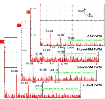
Fig. 11. Spectral analysis of the phase current
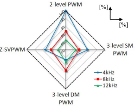
In Fig. 11, at the switching and multiple of the switching frequency (4, 8, 12 kHz), the 3-level PWM strategies stand out in front of the 2-level PWM strategy. As well, the 3-level double modulation method performs better at the frequency of 4 kHz than the simple modulation 3-level PWM but with the price of higher power switching losses. The Z-SVPWM has an almost identical performance as the 3-level SM PWM, with a small advantage present at higher switching frequencies. Comparing the Z-SVPWM to the 3-level DM PWM, it is shown that only at the switching frequency the PWM method is better. In Fig.12, the amplitude spike of the 2-level modulation at 4 kHz has been
iM0 eM0 iM0 uM0 iM1 uM1 uS iS iM1 eM1 TM0+TM1 Ω TM0 Ω TM1 Ω
Zero-sequence fictive machine M0 (harmonics ranks 0, 3, 6, 9, …)
Concordia Transformation Main fictive machine M1
(harmonics ranks 1, 2, 4, 5, 7, 8…) 1 1 0 0 M M M M S S i u i u i u Energy flow iM0 eM0 iM0 uM0 iM1 uM1 iM1 iM1 uM1 uM1 uS iS uS uS iS iS iM1 eM1 iM1 iM1 eM1 eM1 TM0+TM1 Ω TM0+TM1 Ω TM0 Ω TM0 Ω TM1 Ω TM1 Ω
Zero-sequence fictive machine M0 (harmonics ranks 0, 3, 6, 9, …)
Concordia Transformation Main fictive machine M1
(harmonics ranks 1, 2, 4, 5, 7, 8…) 1 1 0 0 M M M M S S i u i u i u Energy flow 0 0,04 0,08 0,12 0,16 -0.2 -0.15 -0.1 -0.05 0 0.05 0.1 0.15 0.2 time [s] S im ul ate d hi gh frequen cy osc ill at ion o f I0 [A ] 2-level PWM 3-level SMPWM 3-level DMPWM Z-SVPWM 0 0,04 0,08 0,12 0,16 -0.25 -0.2 -0.15 -0.1 -0.05 0 0.05 0.1 0.15 0.2 time [s] High fr eq ue ncy o scilla tio n of I0 [A
] 2-levelPWM 3-level SMPWM 3-level DMPWM Z-SVPWM
1.452 p.u.
RMS value RMS value1.116 p.u. RMS value1 p.u. RMS value0.654 p.u.
5% of Imaxf 4 kHz 12 kHz 4 kHz 8 kHz 12 kHz 4 kHz 8 kHz 12 kHz 4 kHz 8 kHz 12 kHz -42 dB -57 dB -67 dB -54 dB -63 dB -67 dB -67 dB -55 dB -64 dB -55 dB -61 dB -70 dB 8 kHz 2-Level PWM 2.5 kHz 10 dB 3-Level-SM PWM Z-SVPWM 3-Level-DM PWM
taken as reference value for the other three modulation methods. With respect to the time constant of the two fictitious machines and for the operating point, the Z-SVPWM has a similar result in terms of harmonic distortion as the 3-level modulations.
Fig. 12. Harmonic distortion percentage as compared to the 2-level PWM method
D2.Impact on the power switching commutation number
Power switching commutations are to be considered when focusing on power losses and heat dissipation. To this purpose the advantage of the proposed Z-SVPWM algorithm allows fewer commutations (decrease by a factor of two) than the classical double modulation 3-level PWM as seen in Fig.13. In this case, the Z-SVPWM strategy looks like a flat-top modulation well known for 3-leg VSI [19].
Fig. 13. Power switching commutations
V- CONCLUSION
The aim of this paper was to present an application of a general space vector approach for a 6-leg VSI. When applied to a PMSM drive, the principle of the developed Z-SVPWM is to supply the stator windings with a specific family of voltage vectors. A deep understanding of the corresponding algorithm has firstly been presented. It is then followed by its FPGA digital implementation. Such implementation has been motivated by the necessity of very short computational time so as to preserve the efficiency of the Z-SVPWM. Experimental results have been provided and a comparison to a classical 2 and 3-level PWM approaches was made. The results show that the Z-SVPWM has the potential to minimize the level of zero sequence current harmonics with a low number of commutations. Future work will present the advantages of the space vector method on the management of the saturation of the VSI. Further implementation for 5-leg VSI can be easily achieved following the same approach.
VI-ACKNOWLEDGEMENTS
The authors would like to thank FUI for the support and funding of the SOFRACI project, as well as OPAL-RT Technologies for the training support.
VII-REFERENCES
[1] J. Holtz, "Pulsewidth Modulation – A Survey" - IEEE Transactions on
Industrial Electronics, vol. 39, n°5, december 1992.
[2] V. Blasko, “Analysis of a hybrid PWM based on modified space vector and triangle-comparison methods”, IEEE Transactions on industry applications, Vol. 33, No. 1, May/June 1997, pp. 756-764.
[3] D-W Chung, J-S Kim, S-K Sul " Unified Voltage Modulation technique for real Time Three-Phase Power Conversion " IEEE Transactions on Industry
applications, Vol. 34, n°2, Mars/April 1998.
[4] A. Dastfan, V.J. Gosbell, Don Platt "Control of a New Active Power Filter Using 3-D Vector Control" IEEE Transactions on Power Electronics, vol 15 n°1, january 2000 p5-12.
[5] A. Julian, G. Oriti, T. Lipo,"Elimination of Common Mode Voltage in three phase sinusoidal Power Converters", IEEE Transactions on Power Electronics, vol 14 n°5, sep1999, p982-989.
[6] P. Delarue, A. Bouscayrol, E. Semail, “Generic Control Method of Multileg Voltage-Source-Converters for Fast Practical Implementation”, IEEE Trans. on Power Electronics, vol. 18, no. 2, March 2003, pp. 517-526.
[7] D. Casadei, D. Dujic, E.Levi, G. Serra, A. Tani, L. Zarri, "General Modulation Strategy for Seven-Phase Inverters With Independent Control of Multiple Voltage Space Vectors", IEEE Transactions on Industrial Electronics, vol.55, no.5, pp.1921-1932, May 2008.
[8] H. M. Ryu, J. H. Kim, and S. K. Sul, “Analysis of multi-phase space vector pulse width modulation based on multiple d–q space concept,” IEEE Trans. Power Electron., vol. 20, no. 6, pp. 1364–1371, Nov. 2005
[9] A. Iqbal, S. Moinuddin, “Comprehensive Relationship Between Carrier-Based PWM and Space Vector PWM in a Five-Phase VSI”, IEEE Transactions on
Power Electronics, Vol. 24, n°10, 2009, pp2379-2390.
[10] E.Levi, D.Dujic, M.Jones, G.Grandi, “Analytical determination of DC bus utilization limits in multi-phase VSI supplied AC drives,” IEEE Trans. on
Energy Conversion, vol. 23, no. 2, 2008, pp. 433-443.
[11] D. Dujic, G. Grandi, M. Jones, E. Levi, "A Space Vector PWM Scheme for Multifrequency Output Voltage Generation with Multiphase Voltage-Source Inverters", IEEE Transactions on Industrial Electronics, vol.55, no.5, pp.1943-1955, May 2008.
[12] X. Kestelyn, E. Semail, "Static Converters chap 8", ISBN. 978-1-84821-195-7, ISTE Ltd and John Wiley & Sons Inc, in press.
[13] E. Semail, C. Rombaut, “New tools for studying voltage-source inverters”,
IEEE Power Engineering Review, Vol. 22. no 3, March 2002, pp. 47-48. [14] E. Semail, C. Rombaut, “New method to calculate the conduction durations of
the switches in a n-leg 2-level Voltage Source”, EPE 2001, 27-29 August, 2001, Graz, Austria, CDROM.
[15] X. Kestelyn, E. Semail, J. P. Hautier, “Multi-phase System Supplied by SVM VSI: A New Fast Algorithm to Compute Duty Cycles”, EPE Journal, vol. 14, n° 3, p. 1–11, 2004.
[16] E. Monmasson, L. Idkhajine, M. N. Cirstea, I. Bahri, A. Tisan, M.W. Naouar, “FPGAs in Industrial Control Applications”, IEEE Trans. on Ind. Informatics, Accepted for publication on May 2011.
[17] E. Monmasson, M. W. Naouar, L. Idkhajine, “FPGA-based Controllers for Power Electronics and Drive Applications”, IEEE Ind. Electron. Magazine, vol. 5, n°1, pp. 1-13, March 2011.
[18] O. Lopez, J. Alvarez, J. Doval-Gandoy, F. D. Freijedo, “Multilevel multiphase space vector PWM algorithm with switching state redundancy”, IEEE Trans.
on Ind. Electron., vol. 56, n°3, March 2009.
[19] L. De Sousa, B. Silvestre, B. Bouchez, “A Combined Multiphase Electric Drive and Fast Battery Charger for Electric Vehicles: topology and Electric Propulsion Efficency Analysis », VPPC’10, IEEE International Vehicular
Power Propulsion Conference, 2010, Lille.
[20] L. De-Sousa, B. Bouchez, “Combined Electric Device for Powering and Charging”, International Patent WO 2010/057892 A1
[21] L. De-Sousa, B. Bouchez, “Method and Electric Combined Device for Powering and Charging with Compensation Means”, International Patent WO 2010/057893 A1.
[22] P. Sandulescu, X. Kestelyn, E. Semail, A. Bruyère, L. De Sousa, B. Bouchez, “A Multiphase Traction/Fast-Battery-Charger Drive for Electric or Plug-in Hybrid Vehicles: Solutions for Control in Traction Mode”, VPPC’10, IEEE
International Vehicular Power Propulsion Conference, 2010, Lille.
[23] S. Lacroix, E. Laboure, M. Hilairet, “An Integrated Fast Battery Charger for Electric Vehicle”, VPPC’10, IEEE International Vehicular Power Propulsion
Conference, 2010, Lille.
[24] A. Hava, R. Kerkman, T. Lipo, “Carrier-based PWM VSI overmodulation strategies: analysis, comparison and design”, IEEE Trans. on Power
Electronics, vol. 13, no. 4, July 1998, pp. 624-689.
[25] D-H Jang, “PWM methods for two-phase inverters”, IEEE Industry
Applications Magazine, March-April 2007, pp. 50-61.
[%] [%] 3-level DM PWM Z-SVPWM Uleft Uright U 0 Uref -Uref U 1