UNIVERSITÉ DE MONTRÉAL
INTEGRATED MICROPHOTONIC-MEMS INERTIAL SENSORS
KAZEM ZANDI
DÉPARTEMENT DE GÉNIE PHYSIQUE ÉCOLE POLYTECHNIQUE DE MONTRÉAL
THÈSE PRÉSENTÉE EN VUE DE L’OBTENTION DU DIPLÔME DE PHILOSOPHIAE DOCTOR
(GÉNIE PHYSIQUE) AVRIL 2013
UNIVERSITÉ DE MONTRÉAL
ÉCOLE POLYTECHNIQUE DE MONTRÉAL
Cette thèse intitulée:
INTEGRATED MICROPHOTONIC-MEMS INERTIAL SENSORS
présentée par: ZANDI Kazem
en vue de l’obtention du diplôme de : Philosophiae Doctor a été dûment acceptée par le jury d’examen constitué de :
Mme SANTATO Clara, Ph. D., présidente
M. PETER Yves-Alain, Dr. Sc., membre et directeur de recherche M. MARTEL Sylvain, Ph. D., membre
DEDICATION
ACKNOWLEDGEMENTS
First of all, I would like to express my gratitude to my research director Yves-Alain Peter for helping me in carrying out my research works. I would like to also thank the members of MPBC Inc. for their collaboration on this work, especially Dr. Roman V. Kruzelecky for his helpful suggestions. I gratefully acknowledge the constructive suggestions of Linh Ngo-Phong from the Canadian Space Agency as well as the financial assistance of the Canadian Space Agency for this work. I am grateful to Dr. Pierre Pottier for his friendly and generous assistance. We had many fruitful discussions especially on the integration of FP with optical waveguides. I also thank Ahmad Hayat for his help in mechanical characterization of FP devices. Many special thanks to Alireza Hajosseini Mesgar for his help in electrical testing of the MEMS comb drive actuator. I am also grateful to him for sharing his experiences and knowledge in times of need. I would like to express my most sincere appreciation to my friend Dr. Alireza Hassani for his assistance in many aspects. He has always been available when I needed help, whether academic or otherwise. I also wish to give my thanks to Philippe Vasseur, Christophe Clément, and Marie-Hélène Bernier for their constructive support in cleanroom. I have learned a lot from them during my Ph. D studies. Also thanks to all other people that have been omitted from the above list, those who have provided aid, support and discussions. Finally, I would like to thank my family for their constant mental support and love. I definitely would not have gotten this far without their love and support.
RÉSUMÉ
Au cours de la dernière décennie, le développement du contrôle d'attitude de petits satellites a évolué vers une stabilisation complète à trois axes et un contrôle précis alors que leur application augmente dans les télécommunications et les missions de connaissance de l'espace. Pour les systèmes spatiaux, les principaux facteurs sont la puissance, la masse et la fiabilité dans l'environnement spatial. Ceci est associé à une nécessité croissante de systèmes de navigation inertielle compacts et de faible puissance. Les systèmes de navigation actuels d'engins spatiaux consistent en différents capteurs et processeurs qui ne sont pas optimisés pour fonctionner ensemble. Cela est coûteux et peut exiger une réduction considérable de la masse et des ressources en puissance disponibles sur un petit engin spatial. Par conséquent, les composants doivent être optimisés par rapport à leur taille, design et procédé de fabrication.
L'objectif de cette thèse est de concevoir, simuler, fabriquer et caractériser des accéléromètres et des capteurs de vitesse de rotation (gyroscopes) planaires miniatures à haute sensibilité et faible coût à base de microsystèmes électromécaniques (MEMS) à bande interdite photonique (PBG) sur un substrat silicium-sur-isolant (SOI) afin d'intégrer un réseau à deux axes de ces capteurs sur une même plate-forme SOI. L'utilisation de dispositifs optiques à guide d’ondes intégrés avec des MEMS sur SOI pour les systèmes de capteurs multicanaux/multifonctions permet l'utilisation de capteurs multiples pour étendre la gamme de mesure et la précision. Cela fournit une redondance essentielle qui rend possible une fiabilité à long terme dans l'environnement spatial, réduisant ainsi la possibilité de défaillance du système. Un navigateur sur puce représente également la capacité à accommoder divers capteurs d'attitude et inertiels sur la même puce afin d'éliminer le besoin de nombreux capteurs séparés. Le produit final présente une réduction de plusieurs ordres de grandeur de la masse et de la taille du système. En outre, la redondance améliore la performance nette et la précision des systèmes de mesure de navigation.
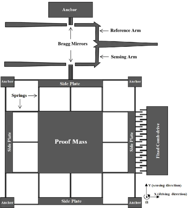
Deux classes d'accéléromètres/gyroscopes optiques sont examinées dans cette thèse pour application dans la navigation de petits satellites, l'une fondée sur un filtre accordable Fabry-Perot (FP), où le capteur est actionné par l'accélération appliquée fournissant un décalage de la longueur d'onde d'opération qui varie linéairement avec l'accélération appliquée, et l'autre fondée sur un atténuateur optique variable (VOA), où le capteur est actionné par l'accélération appliquée fournissant pour les petits déplacements un changement linéaire de l'intensité relative du signal
avec l'accélération appliquée. Dans le cas de capteurs à base de FP, la microcavité FP se compose de deux réflecteurs de Bragg distribués (DBR) dont un miroir DBR est attaché à la masse sismique du système. À la suite d'une accélération/rotation, le déplacement relatif du miroir mobile par rapport au miroir fixe change la longueur de la cavité et modifie la résonance FP. Dans le cas de capteurs à base de VOA, un procédé de modulation d'obturation est utilisé pour moduler l'intensité de la lumière couplée à un guide d'onde multimode en silicium. Un miroir DBR qui est attaché à la masse sismique du système du capteur est positionné dans l'espace entre deux guides d'onde multimodes d'entrée et de sortie. Le déplacement du miroir de Bragg en présence d'accélération/rotation module l'intensité du signal optique transmis entre les guides d'onde d'entrée et de sortie. La sensibilité du capteur est inversément proportionnelle à la largeur des guides d'onde à la jonction du VOA et est inversément proportionnelle à la fréquence de résonance du système.
La principale différence entre les capteurs à base de FP et de VOA présentés ici est que le filtre FP permet une détection optique très sensible du déplacement à une échelle nanométrique, mais nécessite des sources et détecteurs optiques plus complexes, alors que les capteurs à base de VOA n'exigent pas des sources à haute qualité spectrale et la détection est beaucoup plus simple étant donné que l'intensité de la lumière est mesurée à la sortie plutôt que la longueur d'onde. Cependant, pour obtenir un capteur de haute sensibilité, des déplacements au niveau du micromètre sont nécessaires.
Pour les gyroscopes, le capteur utilise un oscillateur à peigne électrostatique de type MEMS pour faire osciller la masse sismique du MEMS le long de l'axe des x à des fréquences de l'ordre de 500 à 1000 Hz. Une rotation appliquée dans l'axe des z provoque le déplacement linéaire de la masse sismique et l'actionneur de détection du VOA / miroir FP mobile, le long de l'axe des y perpendiculaire, proportionnel à la vitesse de rotation. Ce déplacement est modulé alternativement par les oscillations selon l'axe des x, modulant l'actionneur du VOA / l'espacement FP et le signal optique / la longueur d'onde transmise résultante. L'oscillateur électrostatique du MEMS nécessite environ 100 V en courant alternatif pour exciter les oscillations, tel que validé expérimentalement. Cela déplace la masse sismique périodiquement de l'ordre de +/- 3 µm. Ce déplacement n'est pas suffisant pour fournir une modulation élevée du signal optique transmis dans le cas où un VOA est utilisé. Un mécanisme de micro-levier conforme est donc appliqué pour amplifier le déplacement du dispositif de détection à VOA.
même un déplacement de l'ordre du nanomètre peut déplacer de manière significative le pic de transmission du FP. En raison de la conception symétrique de tous les capteurs inertiels présentés ici, ils ont le potentiel d'être conçus comme des capteurs à deux axes.
Des tranches de SOI de différentes épaisseurs sont utilisées en fonction de la performance requise du dispositif et des besoins d'optimisation des procédés. Les étapes de fabrication (procédés de photolithographie et de gravure ionique réactive profonde [DRIE]) ont dû être optimisées à chaque fois que l'épaisseur de SOI a été changée. Pour les tranches de SOI plus épaisses, des résines plus épaisses sont nécessaires comme masque pour le procédé DRIE. L'utilisation de résines épaisses rend la fabrication plus difficile car elle limite la résolution de la photolithographie. Pour chaque épaisseur, les tranchées gravées ont dû être contrôlées par rapport à deux phénomènes bien connus dans le procédé DRIE, à savoir le "scalloping" et le "notching". En particulier, il est très important de minimiser le scalloping sur les parois de silicium, car il génère des pertes optiques par diffusion pour les guides d'onde. Au début de ce travail, du SOI de 30 µm d'épaisseur a été utilisé pour fabriquer les dispositifs. La méthode de couplage bout à bout a été utilisée pour coupler la lumière des fibres optiques aux guides d'onde canaux en silicium. Étant donné que la sensibilité et la résolution du capteur sont proportionnelles à la masse sismique du système, le fait d'utiliser des plaquettes de SOI plus épaisses augmente la masse sismique du capteur pouvant être atteinte, améliorant par conséquent la performance des capteurs. Cela permet également d'intégrer des fibres optiques à la puce et en plus de minimiser les problèmes de désalignement et les instabilités de signal. En outre, cela réduit la sensibilité interaxiale du capteur (en raison d'une raideur interaxiale plus grande). Par conséquent, dans la 2ème phase du projet, du SOI d'épaisseur 47 µm a été choisi pour intégrer passivement des fibres optiques de 80 µm à la puce en utilisant des fentes en U. La masse sismique pouvant être atteinte a été étendue par l'ajout de la masse de la plaquette de Si sous-jacente à la masse sismique du capteur sur la couche du dispositif. Cette approche (que nous appelons “Vertically Extended Mass” (VEM)) peut fournir la plus forte sensibilité d'accélération possible jusqu'à moins de 10 µg. Comme il n'y a pas de substrat sous-jacent, l'approche VEM assure également la plus basse friction possible. Toutefois, la fabrication nécessite deux étapes distinctes de DRIE, et le rendement de fabrication qui en résulte est faible, ce qui nécessite une optimisation additionnelle
de procédé. Pour finir, des tranches de SOI de 75 µm d'épaisseur ont été utilisées pour permettre l'interfaçage des guides d'onde en silicium avec les fibres optiques télécom standards de 125 µm. Contrairement au cas du SOI de 47 µm, pour les cas de SOI de 30 µm et 75 µm, tous les composants du capteur ont été fabriqués en une seule étape de DRIE. Dans le cas du SOI de 47 µm, une plaquette de double SOI a été également utilisée pour guider la lumière uniquement à l'intérieur de la couche supérieure du dispositif, ce qui permet d'avoir des guides d'onde plus minces et ainsi de diminuer la perte optique par diffusion provenant de la rugosité des parois latérales générée pendant le procédé DRIE. Également, avec cette configuration, le phénomène de notching des guides d'onde est évité. Deux types de guides d'onde, à savoir des guides d'onde "rib" et "strip" (canal), sont utilisés pour guider la lumière des fibres optiques au capteur, et vice versa. Pour créer un guide d'onde rib, une autre étape de fabrication est nécessaire sur le dessus du dispositif. Cela nécessite une bonne couverture de résine sur la région de topographie. À cette fin, une nouvelle méthode appelée tension de surface dynamique (DST) a été utilisée dans ce projet.
Des essais mécaniques ont été effectués après chaque libération de dispositif et avant la caractérisation optique en utilisant un montage à sonde afin de s'assurer que le dispositif est complètement libéré.
Les réponses statiques des accéléromètres ont été mesurées en l’exposant à la gravité. L'accéléromètre à base de FP fabriqué sur du SOI de 30 µm a démontré une sensibilité de 2,5 nm/g et une résolution de 4 mg. La performance du capteur a été améliorée en abaissant la fréquence propre du capteur (en utilisant une plus grande masse sismique et des ressorts plus souples), conduisant à une sensibilité de 90 nm/g et 111 µg de résolution pour le capteur. La réponse du capteur est linéaire et sa performance a le potentiel d'atteindre la résolution du µg. L'accéléromètre VEM à base de VOA fabriqué sur du double SOI de 47 µm a démontré avoir une sensibilité de 1.5±0.3 dB/g et une réponse linéaire sur 0,7 g d'accélération appliquée. La sensibilité a été améliorée par un facteur de 2.5±0.3 en réduisant autant la fréquence de résonance que les largeurs des guides d'onde à la jonction du VOA lorsqu’une tranche de SOI de 75 µm d’épaisseur était utilisée comme substrat.
ABSTRACT
Over the last decade, the development of small satellites attitude control has moved towards full three axis stabilization and precise control as their application increases in telecom and space knowledge missions. For space-based systems, the major drivers are power, mass and reliability in the space environment. This is associated with an increasing necessity for compact, low-power inertial navigation systems. Current spacecraft navigation systems consist of various sensors and processors that are not optimized to operate together. This is costly and can require a considerable reduction of the mass and power resources available on a small spacecraft. Therefore the components need to be optimized relative to their size, design, and fabrication process.
The objective of this thesis is to design, simulate, fabricate and characterize high sensitive low cost in-plane photonic-band-gap (PBG)-micro electromechanical systems (MEMS)-based miniature accelerometers and rotational rate sensors (gyroscopes) on a silicon-on-insulator (SOI) substrate in order to enable the integration of an array of two-axis of these sensors on a single SOI platform. Use of guided-wave optical devices integrated with MEMS on SOI for multichannel/multifunction sensor systems allows the use of multiple sensors to extend the measurement range and accuracy. This provides essential redundancy which makes long-term reliability in the space environment possible therefore reducing the possibility of system failure. The navigator microchip also represents the ability of accommodating diverse attitude and inertial sensors on the same microchip to eliminate the need of many separate sensors. The end product exhibits orders of magnitude reduction in system mass and size. Furthermore, redundancy improves the net performance and precision of the navigation measurement systems. Two classes of optical accelerometers/gyroscopes are considered in this thesis for application in smallsats navigation, one based on tunable Fabry-Perot (FP) filter, where the sensor is actuated by the applied acceleration providing a shift in the operating wavelength that varies linearly with the applied acceleration and the other one based on variable optical attenuator (VOA), where the sensor is actuated by the applied acceleration providing a linear change for small displacements around the waveguide propagation axis in the relative signal intensity with the applied acceleration. In the case of FP-based sensors, the FP microcavity consists of two distributed Bragg reflectors (DBR) in which one DBR mirror is attached to the proof mass of the system. As
a consequence of acceleration/rotation, the relative displacement of the movable mirror with respect to the fixed mirror changes the cavity length and modifies the FP resonance. In the case of VOA-based sensors, a shutter modulation method is used to modulate the coupled light intensity to a multimode strip silicon waveguide. A DBR mirror that is attached to the system proof mass of the sensor is positioned in the gap between two input and output multimode waveguides. The displacement of the Bragg mirror in the presence of acceleration/rotation modulates the intensity of the transmitted optical signal between the input and the output strip waveguides. The sensor sensitivity is inversely proportional to both waveguides widths at the VOA junction and system resonant frequency.
The main differences between FP-based and VOA-based sensors presented here is that the FP filter enables a highly sensitive optical detection of displacement at a nanometer scale but requires more complex optical sources and detectors, whereas VOA-based sensors do not require high spectral quality sources and the detection is much simpler since the intensity of light is measured at the output instead of the wavelength. However to obtain a high sensitive sensor, displacements at the level of micrometer are required.
For gyroscopes, the sensor uses a MEMS electrostatic comb-drive with interdigital fingers to oscillate the MEMS proof mass along the x-axis at rates of about 500 to 1000 Hz. An applied rotation in the z-axis causes the proof mass and the VOA sensing actuator/FP movable mirror to be linearly displaced along the perpendicular y-axis, proportional to the rotation rate. This displacement is ac modulated by the x-axis oscillations, modulating the VOA actuator/FP gap and the resultant transmitted optical signal/wavelength. The MEMS electrostatic oscillator requires about 100 V ac to deflect the proof mass periodically by about +/- 3 microns, as validated experimentally. This displacement is not enough to provide high modulation on the transmitted optical signal in the case where VOA is used. Therefore a compliant microleverage mechanism is introduced to amplify the displacement of the VOA sensing device. A two stage micro-lever mechanism is proposed, providing 7 x displacement amplification. In the instance of the FP-based sensor, a compliant structure is not required since even nano-displacement can significantly shift the transmission peak of the FP.
Due to the symmetrical design of all inertial sensors presented here, they have the potential to be designed as two-axis sensors.
process optimization needs. The fabrication steps (photolithography and deep reactive ion etching (DRIE) processes) had to be optimized every time the SOI thickness was changed. For thicker SOI wafers, thicker resists are required as a mask for the DRIE process. Using thick resists make the fabrication more challenging since it limits the photolithography resolution. For each thickness the etched trenches had to be checked for two well-known phenomena in DRIE process namely, scalloping and notching. In particular, it is very important to minimize the scalloping on the silicon walls since they generate scattering optical losses for the waveguides. At the beginning of this work 30 μm thick SOI wafer was used to fabricate the devices. Butt coupling method was used to couple light from optical fibers to the silicon strip waveguides. Since the sensor sensitivity and resolution are both proportional to the system proof mass, using thicker SOI wafers increases the attainable sensor proof mass, consequently improving the sensors performance. This also allows integrating optical fibers to the chip and moreover minimizing the misalignment issues and signal instabilities. Moreover, it reduces the cross-axis sensitivity of the sensor (due to the greater cross-axis stiffness). Therefore in the 2nd phase of the project 47 μm thick SOI wafer was chosen to passively integrate 80 μm optical fibers to the chip using U-grooves. The attainable proof mass was extended further vertically by adding the mass of the underlying Si wafer to the sensor proof mass on the device layer. This method is named as “Vertically Extended Mass” (VEM) approach. This approach can provide the highest achievable acceleration sensitivity to below 10 μg. As there is no underlying substrate, the VEM approach also provides the lowest achievable stiction. However, the fabrication requires two separate DRIE steps and the resulting fabrication yield is low, requiring additional process optimization. Finally 75 μm thick SOI wafers were used to enable interfacing the silicon waveguides to the standard 125 μm telecom optical fibers.
Unlike the case of 47 μm SOI, for the cases of 30 μm and 75 μm SOI, all sensor components were fabricated in one single DRIE step. In the case of 47 μm SOI, a double SOI wafer was also used to guide light only inside the top device layer providing thinner waveguides and therefore lowering scattering optical loss from the side-walls roughness generated during DRIE process. Also with this configuration the notching phenomenon at the bottom of the waveguides is avoided. Two types of waveguides, namely rib and strip waveguides are used to guide the light from optical fibers to the sensor and vice versa. To create a rib waveguide another fabrication
step is required on top of the device. This requires good resist coverage on the topography region. For that purpose a new method called dynamic surface tension (DST) was developed in this project. Mechanical testing was performed after each device releasing and prior to optical characterization by using a probe station setup to ensure that the device is completely released. The static responses of the accelerometers were measured by exposing them to gravity. The FP-based accelerometer fabricated on 30 μm SOI wafer demonstrated 2.5 nm/g sensitivity and 4mg resolution. The sensor performance was improved by lowering the sensor natural frequency (using bigger proof mass and softer springs) leading to 90 nm/g sensitivity and 111g resolution for the sensor. The sensor response is linear and its performance has the potential to reach μg resolution. The VEM VOA-based accelerometer fabricated on 47 μm double SOI demonstrated 1.5±0.3 dB/g sensitivity and a linear response over 0.7 g applied acceleration. The sensitivity was improved by a factor of 2.5±0.3 by reducing both, the resonance frequency and the width of the waveguides at the VOA junction where 75 μm single SOI wafer was used as the substrate.
SUMMARY
Although optical inertial sensors with high performance have been previously reported, none of them is integrated with optical waveguides for in-plane detection purposes. In this work, fully integrated high performance optical MEMS inertial sensors are presented for the first time. All the optical and MEMS components have been integrated on a single silicon-on-insulator (SOI) chip. In-plane optical accelerometers and gyroscopes with two different working principal were successfully fabricated on SOI wafers with different device layer thicknesses. Optical accelerometers were also successfully characterized. These inertial sensors have been designed for micro-satellites navigation purposes where a high performance, compact and low power microchip is required. The most important characteristic of these sensors aside being integrated is their immunity to electromagnetic interferences, making them suitable for space applications. Two different designs with different working principle integrated with optical waveguides are presented. First one is a micro electromechanical systems Fabry-Perot (MEMS FP) based sensor. It is actuated by an applied acceleration to provide a shift in the FP resonance wavelength. Device shows a linear response over its free spectral range with demonstrated 90 nm/g sensitivity and 111g resolution at 450 Hz. Device has the potential to reach μg resolution if larger mass and softer spring is used. The second one is a MEMS variable optical attenuator (VOA)-based sensor. A Bragg mirror that is attached to the sensor proof mass is positioned in the middle of the gap of two optical waveguides: input and output waveguides. When the device is actuated by the applied acceleration, the intensity of the transmitted light from the input waveguide to the output waveguide is modulated by the displacement of the Bragg mirror. Sensor shows a linear response over 0.6 g applied acceleration and 3.4±0.4 dB/g sensitivity. Its performance can be improved by reducing the width of the waveguides at the VOA junction and/or using larger mass and softer springs. The gyroscopes mechanical response was also tested using an integrated MEMS electrostatic comb-drive with interdigital fingers. Device was actuated at 10 Hz frequency for an applied voltage of 100 V leading to 3 µm in-plane displacement. Integration of an array of two-axis of accelerometers and gyroscopes on a single SOI substrate using optical waveguides is possible in future, representing a light, multifunction, low power, high performance, low cost, robust and reliable microchip navigator.
TABLE OF CONTENTS
DEDICATION ... III ACKNOWLEDGEMENTS ... IV RÉSUMÉ ... V ABSTRACT ... IX SUMMARY ... XIII TABLE OF CONTENTS ... XIV LIST OF TABLES ... XVII LIST OF FIGURES ... XVIII LIST OF ABBREVIATIONS ... XXVII LIST OF APPENDICES ... XXXCHAPTER 1 INTRODUCTION ... 1
1.1 History (State-of the-art) ... 7
1.2 Objective of the thesis ... 13
1.3 The situation at the beginning of this work ... 16
CHAPTER 2 THEORY ... 19
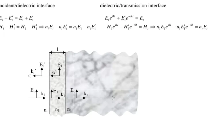
2.1 Fabry-Pérot interferometer with Bragg mirrors ... 19
2.1.1 Finding the reflection and transmission using transfer matrix method ... 19
2.1.2 High reflectance films- concept of Distributed Bragg reflectors (DBRs) ... 21
2.1.3 Fabry-Perot Interferometer (FPI) filter ... 24
2.2 Accelerometers ... 26
2.3 Damping ... 27
2.5.1 Effective finesse and imperfections ... 32
2.5.2 Sensor Dynamic Range ... 34
2.5.3 Sensor Sensitivity ... 34
2.5.4 Sensor Resolution ... 34
2.6 Variable optical attenuator-based accelerometer ... 35
2.6.1 Sources of loss in an optical waveguide ... 36
2.6.2 Modeling of multimode waveguide coupling with shutter modulation ... 37
2.6.3 Sensor Dynamic Range ... 54
2.6.4 Sensor Sensitivity ... 55
2.7 SOI waveguides ... 55
2.7.1 Scattering loss estimation in a strip multimode SOI waveguide ... 57
2.7.2 Optical coupling to silicon waveguides ... 59
2.7.3 Coupling efficiency between a SMF and a multimode waveguide (MMW) ... 62
2.8 Gyroscopes ... 67
2.9 Conclusions ... 74
CHAPTER 3 SYSTEM DESIGN AND SIMULATIONS ... 76
3.1 FP-based optical accelerometer ... 76
3.2 VOA-based optical accelerometer ... 81
3.2.1 Damping ... 84
3.3 Rate Sensor ... 90
3.3.1 Comb Drive Design ... 94
3.3.2 Compliant Mechanisms ... 99
CHAPTER 4 FABRICATION ... 106
4.1 Deep Reactive Ion Etching (DRIE) ... 106
4.1.1 DRIE-Challenges ... 108
4.2 Fabrication Methodology, results and discussion ... 113
4.2.1 30 μm thick SOI process ... 113
4.2.2 47 μm thick SOI-VEM accelerometer process ... 121
4.2.3 75 μm thick SOI Process ... 133
4.3 New Photoresist Coating method for high topography surfaces ... 135
4.3.1 Experiments and results ... 138
CHAPTER 5 CHARACTERIZATION ... 144
5.1 Mechanical characterization ... 144
5.2 Optical characterization ... 146
5.2.1 30 μm thick SOI accelerometers ... 146
5.2.2 47 μm thick SOI-VEM accelerometer ... 153
5.2.3 Optical loss measurements ... 156
5.2.4 75 μm thick SOI ... 159
5.3 Conclusions ... 163
CHAPTER 6 CONCLUSIONS AND FUTURE WORK ... 166
6.1 Conclusions ... 166
6.2 Future Work ... 170
REFERENCES ... 171
PUBLICATIONS RELATED TO THIS WORK ... 183
LIST OF TABLES
Table 1-1: Requirements of accelerometers that are used in current microsats ... 2
Table 1-2: Comparison between our proposed fully integrated optical MEMS accelerometers with some recent developed capacitance MEMS accelerometers and optical MEMS accelerometers. ... 17
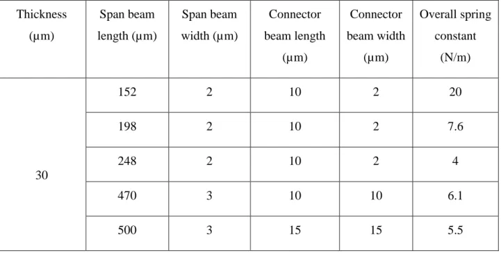
Table 3-1: Serpentine beams components dimensions and the overall simulated stiffness. ... 78
Table 3-2: Span beams dimensions and the overall simulated stiffness. The maximum MEMS displacement for a proof mass with dimensions of 1000 µm×1000 µm is also given. ... 84
Table 3-3: Damping force frequency peak versus gas viscosity. ... 89
Table 3-4: Dimensions of each element used in the sensor ... 94
Table 3-5: Proof mass displacements versus applied voltage to the comb drive in the stationary (quasistatic) regime. ... 97
Table 4-1 Parameters used in DRIE etching ... 108
Table 4-2: A comparison between DST technique and three others techniques. ... 136
Table 5-1: Accelerometer design parameter used in Figure 4-11. ... 149
Table 5-2: Average power fluctuation, average line slope and line slope fluctuation of the VOA-based accelerometer sensor over four days of measurement. ... 162
LIST OF FIGURES
Figure 1-1: (a) Analog devices MEMS capacitance dual-axis accelerometer ADXL210A, (b) Coplanar MEMS capacitance accelerometer, Silicon Design SD2012-10 [2]. ... 4 Figure 1-2: Single-chip CMOS-MEMS capacitance accelerometer with microgravity sensitivity:
(a) schematic illustration of the sensing element, (b) SEM view of the fabricated device [3].5 Figure 1-3: (a) Working principal of a MEMS-based gyroscope, (b) Schematic view of the
gyroscope reported by H. Yang [6]. ... 6 Figure 1-4: ARROW-based optical accelerometer operational principle [20]. ... 7 Figure 1-5: FP-based optical accelerometer working principle reported by [37]. ... 8 Figure 1-6: Schematic of the FP-based optical accelerometer presented by Schröpfer et al. [26]. . 8 Figure 1-7 : Schematic of the FP-based optical accelerometer presented by J. John et al. [21]. ... 9 Figure 1-8: a) Schematic of the working principle of the silicon MEMS-based optical
accelerometer, and b) SEM image of the fabricated device reported by B. Guldimann [43]. ... 10 Figure 1-9 : Out-of-plane rotational rate sensor based on capacitance measurement between the
movable mass and the substrate [29]. ... 11 Figure 1-10 : Yaw rate sensor reported by M. Lutz et al. [32]. ... 11 Figure 1-11: 3-axis gyroscope (Beating Heart) and 3-axis accelerometer fabricated on the same
silicon die [4]. ... 12 Figure 1-12: 6-axis inertial motion sensor in 3×5.5×1 mm3 package fabricated on two different
silicon dice and assembled with the companion CMOS chip [4]. ... 13 Figure 1-13 : Conceptual design of two-axis spacecraft navigation micro-PIC system. ... 15 Figure 2-1: Wave vectors and their associated electric fields for the normal incidence case on a
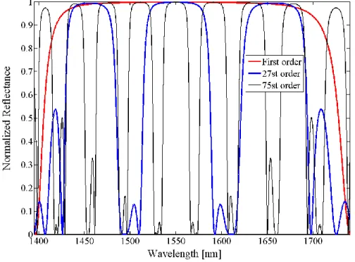
single dielectric layer ... 20 Figure 2-2: Normalized reflectance versus wavelength for a three layer grating with three
wavelength. ... 24 Figure 2-4: The full characteristic transmittance pattern of a FPI. ... 25 Figure 2-5: Accelerometer modeled as a mass-spring-damper system. ... 27 Figure 2-6: Normalized frequency response of a second order system for different damping ratio. ... 29 Figure 2-7: Three types of damping: (a) squeezed-film translational damping, (b) slide-film
damping, and (c) squeezed-film rotational damping. ... 30 Figure 2-8: (a) FPI with different gap between reflective Bragg grating mirrors, (b) Mechanical
block mass-spring-damper model of a FPI-based sensors, and (c) Transmission curve shift of a FPI due to changes in gap between two mirrors. Two FPI orders are considered (with
m=1 and m=2). ... 31
Figure 2-9: (a) Transmission versus wavelength of a resonance with mechanical defects of the mirrors (parallelism, roughness, spherical bowing), (b) List of values for each defect type and finesse. PS: as finesse value increases, the fringe becomes narrower, (c) Schematic of different types of mechanical defects [50]. ... 33 Figure 2-10: Shutter modulation based on transmission mode ... 35 Figure 2-11: Schematic of light propagation in a step index waveguide. is the maximum
acceptance angle with respect to the waveguide axis at which light rays can propagate and still be guided by total internal reflection. Any light entering with angles greater than will be quickly lost through radiation or leaky modes. ... 38 Figure 2-12: Schematic view of our multimode rectangular waveguide. The top and bottom walls
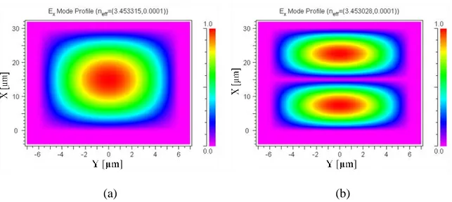
are smooth and only the sidewalls have roughness. ... 39 Figure 2-13: Simulated intensity distribution of first two modes of a multimode SOI strip
waveguide with 2d (width) =12 µm, 2b (height) = 30 µm: (a) Fundamental mode, (b) first even-odd mode (01 mode). ... 45 Figure 2-14: Longitudinal coupling loss variation as a function of longitudinal distance between
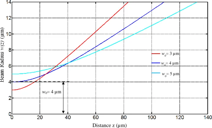
Figure 2-15: Divergence of a Gaussian beam as it travels for three different value of initial beam radius (λ=1550 nm). ... 48 Figure 2-16: Schematic of the optical model for VOA-based sensors ... 49 Figure 2-17: Normalized transmitted power as a function of mirror position for three different
beam radiuses seen at the mirror position. Black solid lines are the lines fitted on the curves at the initial mirror position . Dotted lines are the lines fitted on the curves to calculate the linear range response of device with 5% uncertainty. ... 52 Figure 2-18: Attenuation in power output versus mirror position for VOA- based sensor devices
for three different beam radiuses seen at the mirror position. ... 54 Figure 2-19: Various types of SOI waveguides: (a) rib waveguide; (b) strip waveguide ... 55 Figure 2-20: a) Cross section of rib waveguide, b) Simulated intensity distribution of the
fundamental TE mode of a single mode SOI rib waveguide with W=10 µm, H= 15 µm, and h=12 µm. ... 57 Figure 2-21: In a silicon strip waveguide fabricated on SOI substrate, upper and lower interfaces
of waveguide have smooth surfaces compared to sidewalls. As a result to estimate the scattering loss, the waveguide can be approximated with a planar waveguide constituting of sidewalls. ... 57 Figure 2-22: Propagation of mode in a planar waveguide. ... 58 Figure 2-23: Reflection and transmission for the normal incidence case at the interface of
mediums i and t. Wave vectors and their associated electric fields are shown. ... 60 Figure 2-24: Coupling between two Gaussian beams. In this case, the incident beam is the output
beam of a SM fiber coupled to the mode of a SM waveguide. ... 61 Figure 2-25: Different sources of optical coupling loss from an optical fiber to a Si waveguide:
(a) reflection loss caused by reflections between fiber and waveguide facets, (b) mode mismatch between coupled modes, (c) silicon waveguide facet roughness causing scattering loss, (d) loss due to longitudinal offset between fiber and waveguide, (e) loss generated by transversal offset between fiber and waveguide, and (f) loss generated by angular misalignment between fiber and waveguide. ... 62
Figure 2-27: Coupling efficiency between a SMF and two different MMF with core radii of 52.5
µm and 92.5 µm as a function of mode number [109]. ... 67
Figure 2-28: Working principle of a MEMS gyroscope ... 68
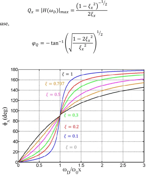
Figure 2-29: Phase angle plotted against the frequency ratio for various levels of damping ... 70
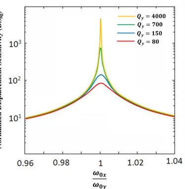
Figure 2-30: Normalized displacement sensitivity of the gyroscope versus ω0x/ ω0y for different values of Qy ... 73
Figure 3-1: Schematic of the optical accelerometer based on FP filter ... 76
Figure 3-2: Finite element simulation of the optical accelerometer structure containing eight serpentine flexures beams. The red region is proof mass of the sensor. ... 77
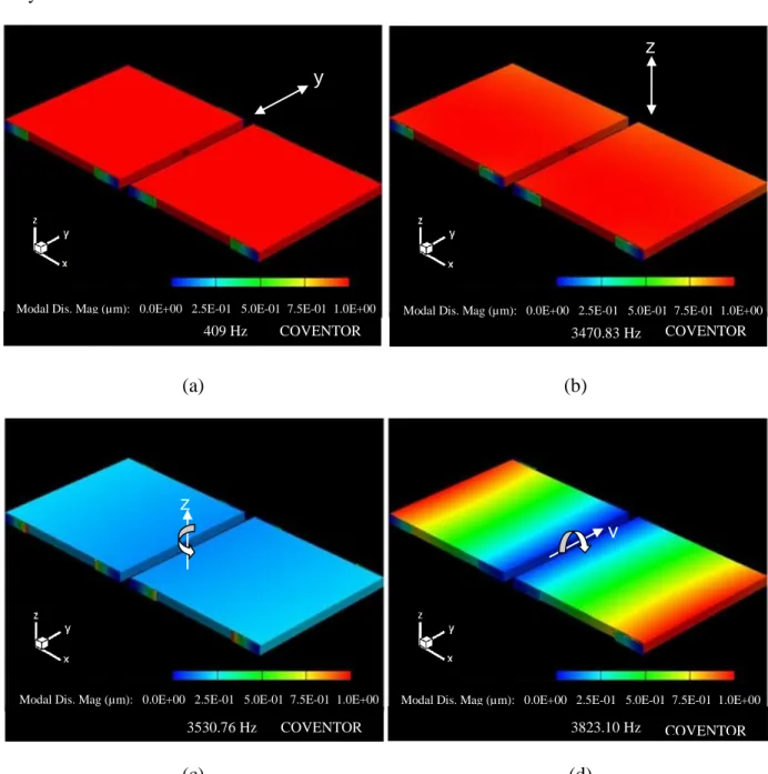
Figure 3-3: Simulated first four modes of the device: a) Normal mode (excited at 409 Hz), b) Second mode (excited at 3.48 kHz), c) third mode or trunnion mode (excited at 3.53 kHz), and d) Forth mode (excited at 3.82 kHz). The arrows in the pictures show the displacement (or rotation) for each mode. ... 80
Figure 3-4: Two expected sensitive modes for the sensor. ... 81
Figure 3-5: Simulated frequency response of the system to a constant acceleration for the normal and trunnion modes. ... 81
Figure 3-6: Schematic of the optical accelerometer based on VOA. ... 82
Figure 3-7: Simulated damping force, spring force, and damping coefficient of squeezed-film translational damping as a function of frequency for two different gaps: (a), (c) 150 µm and (b), (d) 20 µm, gas: air. ... 88
Figure 3-8: (a) Damping coefficient as a function of frequency in the case of Slide-Film Damping (gap=100 µm), and (b) Damping and spring torque as a function of frequency for the case of Squeezed-Film Rotational Damping (gap=20 µm), gas: air. ... 89
Figure 3-9: Schematic view of the designed rate sensor based on FP ... 90
Figure 3-10: Schematic view of the designed rate sensor based on VOA ... 91
Figure 3-12: Maximum driving displacement of the sensor versus the applied voltage to the comb drive for three different values of quality factors in driving direction. ... 96 Figure 3-13: Effect of x-cross sensitivity on the transmitted light at the VOA junction. ... 97 Figure 3-14: Electrostatic simulation result of the rate sensor. Maximum x displacement of the
structure is 2.1 µm when 200 volts voltage is applied. ... 99 Figure 3-15: Classification of three kind of micro-lever ... 101 Figure 3-16: Two-stage micro-lever used dimensions ... 102 Figure 3-17: FEM simulation of the rate sensor, (a) without and (b) with two stage micro-lever.
Same forces are applied in both cases. The structure response without and with leverage mechanisms to the applied force is 1.7 μm and 12 μm respectively, resulting in 7 x displacement amplification. ... 103 Figure 3-18: Two stage micro-lever integrated with gyroscope (fabricated on 47 µm SOI). ... 103 Figure 4-1: Schematic of Bosch process in DRIE: (a) Etch step using SF6 gas, (b) Side wall
passivation using C4F8, (c) Etch cycle using SF6 gas after passivation. ... 107 Figure 4-2: Etched trenches into SOI substrate: (a) sidewalls with poor verticality, and (b) good
verticality ... 109 Figure 4-3: Scalloping phenomenon in DRIE: (a) An etched trench in silicon, (b) Etched rib
waveguide, the scalloping can be seen on the rib waveguide’s side walls. ... 110 Figure 4-4: Trenches etched in SOI substrate, (a) High aspect ratio structures etch more slowly,
leading to notching (b) at the silicon and oxide interface when a SOI wafer is used. This can result in an unwanted releasing of small features in the pattern (c). ... 111 Figure 4-5: Notching observed on the finger of the comb drive of a rate sensor. ... 112 Figure 4-6: Formation of micro-grasses in (a) SOI, and (b) Silicon substrate. As seen in (b), this
can stop the etching process. ... 113 Figure 4-7: Fabrication process of optical accelerometers integrated with rib waveguides. Devices
are fabricated on a SOI substrate with 30μm-thick device layer. ... 115 Figure 4-8: A FP-based optical accelerometer after second photolithography ... 117
Figure 4-10: Microfabrication steps for the FP and VOA based accelerometers integrated with strip waveguides, fabricated on SOI substrate with 30μm-thick device layer. ... 118 Figure 4-11: SEM photograph of the silicon microfabricated FP-based accelerometer integrated
with strip waveguides. ... 119 Figure 4-12: (a) SOI waveguide facet after polishing, and (b)Three-dimensional AFM image of
the waveguide’s facet surface profile after polishing. ... 119 Figure 4-13: Optical images of two different samples after releasing process (a) sample was
exposed to vapor HF for long time leading to waveguides lift up, and (b) Sample that has been released with optimized releasing time. A part of waveguide was broke to check the remaining oxide layer under the strip waveguide. ... 120 Figure 4-14: Alignment between fiber and input waveguide ... 122 Figure 4-15: Dimensions of used double SOI ... 124 Figure 4-16: Fabrication process for optical accelerometers using double SOI: (a) 2 µm oxide
layer deposition on the front side of the wafer to protect it during the fabrication on the backside, (b) Cr deposition and lift-off on the backside, (c) DRIE on the backside until the bottom BOX layer is reached, (d) removing the sputtered oxide protection layer followed by photolithography on the front side, (e) DRIE on the front side until the bottom BOX layer is reached, and finally (f) resist stripping followed by proof mass releasing using vapor HF from the backside. ... 126 Figure 4-17: An array of 2 µm etched trenches. Presence of grasses at the bottom of the trenches
slows down the etching process. ... 127 Figure 4-18: Photograph of several VOA accelerometer devices after the 500 µm backside DRIE
of SOI for the case of VEM approach. ... 127 Figure 4-19: SEM photograph of 500 µm backside DRIE of SOI for VEM approach, (a) Side
Figure 4-20: SEM photograph of the fabricated VEM VOA-based optical accelerometer with added mass from Si handle on 47 µm double SOI. Inset: close up view of the Bragg shutter. The width of the input and output waveguides are 20µm. ... 128 Figure 4-21: (a) Integrated input U-groove with added staggered dams, and (b) Right-angle
waveguide bend, showing smooth waveguide sidewalls in the 15 micron top Si device layer with some roughening in the lower 32 micron-thick middle Si device layer. ... 129
Figure 4-22: (a) Fabricated VOA-based gyroscope integrated with two stage micro-lever on 47 µm double SOI, (b) close up of the device. ... 130
Figure 4-23: (a) Close up of the VOA sensing junction of the fabricated VOA-based gyroscope on 47 µm single SOI, (b) Input waveguide and its associated U-groove (for optical fiber to silicon waveguide light coupling). ... 131 Figure 4-24: An array of trenches with 50 µm depth and different widths covered by a thick layer
of resist SPR 220-7.0. (a) Bubbles are formed after soft baking due to resist solvent evaporation. (b) Some cavities are observed after resist spinning and soft bake. ... 131 Figure 4-25: (a) Photograph of a sample with 47 µm topography coated with thick resist after
UV-exposure, (b) Same sample after DRIE. ... 132 Figure 4-26: Photograph of a sample after resist spinning. Springs get broken due to the
centrifugal force. ... 132 Figure 4-27: SEM photograph of the VOA-based optical accelerometer fabricated on 75 µm SOI.
Strip waveguides widths at the VOA sensing junction interface are tapered to 12 µm to increase the sensor sensitivity. ... 134 Figure 4-28: SEM photograph of the VOA sensing junction fabricated on 75 µm SOI. Strip
waveguides at the VOA sensing junction interface are anchored to the substrate to prevent them from lifting after releasing the oxide layer. ... 134 Figure 4-29: VOA-based gyroscope integrated with two stage micro-lever fabricated on 75 µm
SOI. ... 135 Figure 4-30: An array of trenches with resist coated by spinning method. ... 136 Figure 4-31: a) Coated AZ9260 resist diluted with butyl alcohol, b) zoom on one trench. ... 138
Figure 4-33: a) Coated AZ9260 resist diluted with acetone, b) zoom on one trench. ... 139 Figure 4-34: Coated SPR 220-3.0 resist. ... 141 Figure 4-35: The entire edge of an array of trenched. Resist cannot be suspended over the
trenches with large widths. ... 141 Figure 4-36: Photolithography on the suspended resist over the trenches coated by DST method. ... 142 Figure 4-37: Etched sample after photolithography and DRIE. ... 142 Figure 4-38: (a) Schematic of the photolithography process on the coated SPR 220-3.0
photoresist (using DST method) on a structure with pre-existing topography (array of trenches), (b) Sample after photolithography, DRIE and resist stripping. ... 143 Figure 5-1: Probe station setup for sample release testing. ... 144 Figure 5-2: Release testing of a VOA accelerometer with a needle. ... 145 Figure 5-3: Mass displacement of a VOA accelerometer for different actuator frequencies. ... 145 Figure 5-4: Experienced acceleration versus the actuator frequency. ... 146 Figure 5-5: Optical setup for the characterization of the accelerometers. ... 147 Figure 5-6: Measured (colored curves) and simulated (black curves) transmission spectra of the
FP-based accelerometer integrated with strip waveguides for various accelerations (ωn=10.5 kHz). ... 148 Figure 5-7: Measured wavelength shift versus applied acceleration of the FP-based accelerometer
integrated with strip waveguides (ωn=10.5 kHz). ... 148 Figure 5-8: Measured (colored curves) and simulated (black-dashed curves) transmission spectra
of the FP based accelerometer integrated with strip waveguides for various accelerations (ωn= 2.75 kHz). ... 150 Figure 5-9: Measured wavelength shift versus applied acceleration of the FP-based accelerometer
Figure 5-10: Measured transmission spectra of the FP-based accelerometer integrated with rib waveguides (ωn= 17.7 kHz). ... 152 Figure 5-11: wavelength shift versus applied acceleration of the FP-based accelerometer
integrated with rib waveguides (ωn= 17.7 kHz). ... 152 Figure 5-12: Static response of the VEM VOA-based accelerometer to applied acceleration
(ωn= 4.1 kHz). ... 154 Figure 5-13: Gyroscope drive mode testing by applying differential voltage between the movable
and the fixed part of the comb drive, (a) 47 µm single SOI device, and (b) 47 µm double SOI test structure, the top device layer (waveguide layer) has been etched partially to reach the middle device layer (actuator layer). ... 156 Figure 5-14: SOI fabricated waveguides with different length integrated with U-grooves. ... 157 Figure 5-15: Waveguide transmission versus waveguide length for 47 μm thick single SOI
device. ... 158 Figure 5-16: Waveguide transmission versus waveguide length for 47 μm thick double SOI
device. ... 158 Figure 5-17: (a) Sample glued to the optical fibers mounted on the optical setup, (b) Close up
view of sample. ... 159 Figure 5-18: (a) Epoxy reservoir integrated with U-groove and fiber filled by UV-curing optical
adhesives, (b) SEM of the bonded optical fiber to the input waveguide after curing. Staggered dams are indicated in the picture. ... 160 Figure 5-19: SEM photograph of the VOA-based optical accelerometer fabricated on 75 µm SOI.
Strip waveguides widths at the VOA sensing junction interface are tapered to 12 µm. ... 160 Figure 5-20: The static responses of the 75 µm thick VOA-based accelerometer (having a natural
resonance frequency of ωn= 2.14 kHz) to applied accelerations measured at four different days. ... 162
LIST OF ABBREVIATIONS
⃗ Electric field ⃗⃗ Magnetic field n Refractive index Wave vector r Reflection coefficient t Transmission coefficient R Reflectance T Transmittance λ wavelength Gap of Fabry-Perot Order of Fabry-Peroth Order of Bragg mirror
F Finesse
Full width at half maximum
b Damping factor M Mass k Spring constant ω Angular frequency Δx Displacement µ Medium viscosity ξ Damping ratio a Accelaration
Rayleigh range P Optical power L Optical loss Ω Angular rotation Q Quality factor E Young’s modulus Beam length
Number of fingers of a comb drive
V Applied voltage Vacuum permittivity
INDICES
1 Medium 1 2 Medium 2 c Coriolis (Force) D Driving (Frequency) eff EffectiveH High refractive index
i Medium i
L Low refractive index
n natural (Frequency)
p Mode p
q Mode q
R Reflectance
ABBREVIATIONS
VEM Vertical Extended Mass AFM Atomic force microscopy DBR Distributed Bragg reflectors DRIE Deep reactive ion etching DST Dynamic surface tension EMI Electromagnetic interference FOG Fiber optical gyroscope
FP Fabry-Perot
FPI Fabry-Perot interferometer FSR Free spectral range
FWHM Full width at half maximum MEMS Microelectro-mechanical systems micro-PIC Microphotonic integrated circuits
NA Numerical aperture
OSA Optical spectrum analyzer PBG Photonic-band-gap
RLG Ring laser gyroscope
SEM scanning electron microscopy SMF Single mode fiber
SOI Silicon on insulator
VOA Variable optical attenuator WHU Wafer handling unit
LIST OF APPENDICES
Appendix 1: Design parameters for VOA-based accelerometer fabricated on 75 µm-thick SOI substrate………184
CHAPTER 1
INTRODUCTION
Microphotonics is a new technology using miniaturized photonic elements with wafer-level integrated systems which sense, emit, and transmit light and other forms of energy with photon as quantum unit. Microphotonics technology is comprised of a variety of new devices, materials, processes, namely Photonic Integrated Circuits (PICs), Micro Opto Electromechanical Systems (MOEMS), Photonic-Band-Gap structures (PBGs), smart materials, and quantum photonic system.
Microphotonic integrated circuits (micro-PICs) are the integration of two or more photonic devices on a single substrate alike microelectronic chips. Nevertheless, instead of guiding electricity, a micro-PIC transmits light beams. The main difficulty that microphotonics should solve is system integration. Integrating different optical components on a unique substrate, will contribute in reducing the amount of external fiber optic interconnections, consequently decreasing the overall system mass and size, and contributing the optimization of the system reliability as well as its cost efficiency. Many fields use microphotonics technology for their operations, namely: space, medicine, telecommunications, security and military. The application of microphotonics technology in space has to recognize the specific needs of the space industry, the space operational field as well as the technical feasibility. Based on the systems needs for space, the components need to be optimized relative to their size, design, and fabrication process. Over the last decade, the development of small satellites attitude control has moved towards full three axis stabilization and precise control as their application increases in telecom and space knowledge missions. This results in an increasing need for compact, low-power inertial navigation systems. An inertial navigation system (INS) is a combination of motion sensors (accelerometers) and rotation sensors (gyroscopes). The navigation is accomplished by integrating the output of the sensors to continuously calculate the position, orientation, and velocity (direction and speed of movement) of the satellite. Accelerometers measure linear acceleration with respect to an inertial frame and gyroscopes (angular rate sensors) measure angular rotation rates with respect to an inertial space. Essentially, an INS contains three accelerometer and three gyroscopes as an arbitrary motion in space requires six degree of freedom. Satellite navigation system can take advantage of implementing PIC and micro-electro-mechanical systems (MEMS) technologies. The integration of PBGs with MEMS
(PBG/MEMS) and guided-wave optics on a single platform present new feasibilities for miniature space systems that have a significant effect on system performance, size, weight, data integrity, power consumption and lowering the cost of space-based systems [1]. Table 1-1 summarizes the requirements of accelerometers being used in the current microsats based on their missions.
Table 1-1: Requirements of accelerometers that are used in current microsats
Parameter Requirement Mission/
Microsat.
Sensor Requirement
Position Accuracy +/-300 m over 45 min. Measurement time
per orbit
Nadir Earth
Observation < +/- 0.010 mg
Cross-axis sensitivity 1% is current performance
for best MEMS capacitance sensors Typical acceleration
levels for satellite in orbit
1 to 50 mg 100 mg full scale
should cover most in-orbit acceleration (except the launching) Launch vibration
levels
<11 g rms typically
Proba 2 About 20 g peak
Frequency range of operation 1-10Hz for navigation control of typical spacecraft 10 Hz sensor measurement rate Operating temperatures -40 oC to +60 oC Proba-2 -40 oC to +60 oC
There are mainly two technologies being considered as platforms, namely Silicon-On-Insulator (SOI) and Indium-Gallium-Arsenide-Phosphide (InGaAsP). The principal differences between the two platforms are higher costs and less experimented fabrication technologies for the III-V compound semiconductors. Currently, the SOI platform is widely being used because of its compatibility with high-speed CMOS integrated electronics making the fabrication process easier. Also the size of the integrated optical structures is smaller due to the high index contrast between silicon and air. Consequently, in most cases, the SOI would constitute the preferred choice of substrate for integrating the microphotonics technologies for diverse space applications.
earliest large scale application is in automotive industry, where they are used in the air bag system. In micro scale, they have much broader applications such as in: consumer products such as camcorders to stabilize the image, three-dimensional mousses, laptop and tablet computers, mobile phones and remote controllers, games, toys, etc; biomedicine such as activity monitoring;
industry such as robotics, vibration monitoring in machines, and shock monitoring for goods
transportation; geology such as scientific research of earthquakes; military such as accurate guidance in missiles and other ordnance, aircrafts; space such as inertial navigation applications. In the latter case, very high resolution in the order of micro-gravity is required. This type of accelerometers manufacturing is very challenging due to their high required performance. They are also used in geophysical and oil-field applications. Today maybe the largest market for the motion sensors application is in smart phones such as i-phones (allowing the device to know when it is tilted on its side) and location based services (GPSs). Indeed, accelerometers in recent years have become the world’s hottest electronic products making them the top selling MEMS devices. Especially when they are combined with short range radio sniffers like Wifi, they provide a marvelous navigation for the users.
There are four main kinds of accelerometers, piezoresistive accelerometers, piezoelectric accelerometers, capacitive accelerometers, and optical accelerometers. In a piezoresistive accelerometer, piezoresistors are placed on suspension beams. As the support frame moves due to the external acceleration, the suspension beams bend resulting in a change of the resistivity of their embedded piezoresistors. In a piezoelectric accelerometer, when a piezoelectric material is stressed, an electrical charge signal is generated as a function of acceleration. On the other hand, in capacitive accelerometers, capacitance between the sensor proof mass and a fixed conductive electrode changes as a function of acceleration. Capacitive accelerometers provide several benefits compared to piezoelectric/piezoresistive accelerometers namely, high sensitivity, good noise performance, and low temperature sensitivity [2]. The method of acceleration detection in capacitive and piezoelectric/ piezoresistive accelerometers is based on electrical detection and therefore they are not immune to electromagnetic interferences (EMI). Unlike them, optical accelerometers are based on optical detection hence they are immune to EMI. These types of accelerometers will be addressed in the next section (1.1).
MEMS capacitance accelerometers are currently used in the navigation systems of spacecraft. Figure 1-1 shows two types of MEMS capacitance accelerometers; Analog Devices MEMS capacitance accelerometer and coplanar MEMS capacitance accelerometer. Analog Devices MEMS sensors are based on surface micromachining techniques and therefore offer the opportunity to integrate the sensor and interface circuitry on a single chip. In these devices, the deflection of the structure due to an input acceleration is measured using a differential capacitor. For example ADXL210A (Figure 1-1 (a)) is a polysilicon surface-micromachined dual-axis accelerometer built on top of a silicon wafer. Since surface micromachined accelerometers have small proof mass they suffer from high mechanical noise (mechanical noise is inversely proportional to proof mass) and low resolution. Coplanar MEMS capacitance accelerometer is a z-axis accelerometer (Figure 1-1 (b)) consisting of an underlying fixed electrode and a suspended electrode that can tilt in response to the applied acceleration.
Zhang et al. [3] have developed a single-chip CMOS-MEMS capacitance accelerometer with microgravity sensitivity. The sensor is fabricated on a SOI wafer and integrated with CMOS interface circuit. In order to get a high sensitivity the handle layer of the wafer is used to build the proof mass while the springs are defined on the device layer ( Figure 1-2). Sensor has the ability to measure accelerations in µg range.
(a) (b)
Figure 1-1: (a) Analog devices MEMS capacitance dual-axis accelerometer ADXL210A, (b) Coplanar MEMS capacitance accelerometer, Silicon Design SD2012-10 [2].
(a) (b)
Figure 1-2: Single-chip CMOS-MEMS capacitance accelerometer with microgravity sensitivity: (a) schematic illustration of the sensing element, (b) SEM view of the fabricated device [3]. Regarding the gyroscopes, there are essentially three types of gyroscopes that are extensively employed today for inertial navigation and rotation rate sensing. The selection of the type of gyroscope for any particular application depends on the performance and cost requirements and also the fabrication complexity. Firstly, there are capacitive MEMS gyroscopes which are light, easy to fabricate and have a relatively high performance however they are not immune to EMI and usually sensitive to the mechanical vibration and acceleration. MEMS silicon-gyroscopes have no exact life-limiting features due to their low power consumption, resulting in a long life of more than 15 years for space applications [5]. Figure 1-3 (a) shows a principal operation of a gyro MEMS-based. A suspended mass is excited in one dimension (x in this figure) and the out-of-plane (z direction) vibration is induced by the rotation due to the Coriolis force leading to the capacitance change between the suspended mass and the substrate. The amount of this capacitance change is then electrically sensed and converted to a rotation rate. Device can also be driven into vibration in both the x and y-directions, and the angular rate is measured by detecting the phase variation in the lateral vibration signal [6]. Figure 1-3 (b) shows a gyroscope developed by H. Yang based on this concept.
(a) (b)
Figure 1-3: (a) Working principal of a MEMS-based gyroscope, (b) Schematic view of the gyroscope reported by H. Yang [6].
Secondly and thirdly, ring laser gyroscope (RLG) and fiber optical gyroscope (FOG) whose working function are based on the Sagnac effect. The Sagnac effect states that, when two beams of light propagate in the opposite directions along a common path in a rotating frame of reference, these beams experience a phase difference which is proportional to the rotational rate. RLG and FOG gyroscopes provide very high dynamic range and sensitivity. They are also accurate, robust, and immune to mechanical vibrations but they are very difficult to manufacture and expensive. In addition, RLGs are heavy and not appropriate for smallsats applications. A RLG weigh typically is 20 pounds.
Among all, optical accelerometers and gyroscopes offer advantages in comparison to electrical-detection -based sensors because of their:
• Immunity to electromagnetic interference (EMI)
• Insensitivity to charging that can occur in the space environment • Simple MEMS micromechanical structures
• High dynamic signal measurement range • Resistance to aggressive environments • Electrical and fire safety
• Small, lightweight sensing elements allowing arrays of sensors on an SOI microchip
These characteristics make them a good candidate to be used for the space navigation system.
Seismic mass
.
X Ω Z Anchor Anchor Anchor Anchor1.1 History (State-of the-art)
To our knowledge, the first optical accelerometer using optical fiber and micromachined structures was reported in 1984 [8], [9]. Subsequently, a large range of fiber optic and waveguide-based micromachined accelerometers were reported. Most of them are based on Variable Optical Attenuator (VOA) [10], [11], [12], [13], [14], interferometric [15], optical diffraction detection [16], [17], [18] , Anti Resonant Reflecting Optical Waveguides (ARROW) [19], [20] or wavelength dependent [26], [27], [28], [37] methods. Although some of them are very sensitive [14], [16], [17], [37], none of them is designed simultaneously for in-plane detection and compactness, consequently they cannot be integrated with other optical functions. Some of the most recent optical-MEMS-based optical accelerometers will be discussed briefly here. Fiber Bragg grating (FBG) acceleration sensors have also been reported by several groups [40], [41], [42]. Although in some cases FBG can reach a relatively high sensitivity (77 pm/g) [40], the optical fibers need manual positioning and cannot be integrated with other optical structures on a planar chip.
Figure 1-4 shows an optical accelerometer based on Anti Resonant Reflecting Optical Waveguides (ARROW) developed by J. A. Plaza, et al.[20]. A waveguide, which is the sensing part of the device, is attached to the seismic mass of the accelerometer and is aligned with two other waveguides on the silicon frames. When there is an offset of the mass due to the acceleration, the transmitted light intensity at the output is modulated, and an intensity loss is generated, which is used to measure the acceleration. The device sensitivity is different for different directions (2.3 dB/g for negative and 1.7 dB/g for positive acceleration). The acceleration resolution is not reported. This device is designed for out-of-plane detection.
Figure 1-5 shows another approach presented by A. Perez and A. M. Shkel [37].This device is based on Fabry-Perot (FP) interferometer and consists of two deep reactive ion etched silicon substrates that are assembled to create a FP optical cavity. These two silicon substrates act as the FP mirrors and are coated with quarter wavelength multilayer reflector of silicon dioxide, amorphous silicon and silicon nitride to increase the mirror reflectivity.
Figure 1-5: FP-based optical accelerometer working principle reported by [37].
One of the mirrors is composed of proof mass and flexure beams created by deep reactive ion etching (DRIE). The device has high sensitivity and resolution (1V/g and 30 µg respectively) but it is bulky (as it is composed of two different silicon wafer bonded by spacers), not integrated on a single chip, and has been designed for out-of-plane vibration detection purposes.
In 1998, a fiber optic based accelerometer (Figure 1-6) using a FP as the sensing element was presented by Schröpfer [26].
between the accelerometer proof mass and the fiber facet provides a low finesse FP cavity. The deflection of the proof mass relative to the fixed fiber in the presence of an inertial load causes a shift in the transmitted wavelength of the FP interferometer. Device has a low sensitivity due to the low reflectivity of the FP mirrors (fiber facet and seismic mass vertical wall). Sensor resolution is 1 mg for a measurement range of ±10g.
J. John et al. [21] have used a similar structure for the inertial navigation system application in spacecrafts; except that two fibers are employed instead of one at both sides of the seismic mass, providing a differential detection measurement. The seismic mass is a silicon cantilever formed by bulk micromachining technique suspended by four beams (Figure 1-7). Since a differential measurement is used, the signal level is doubled in this configuration. The reported sensitivity is in the mili-g order with a dynamic range of ±12 g.
Figure 1-7 : Schematic of the FP-based optical accelerometer presented by J. John et al. [21]. Another optical method to measure the acceleration is based on the measurement of an optical modulation caused by proof mass called variable optical attenuator (VOA). Optical accelerometers based on intensity modulation were proposed [10], [11], [12]. Some of them are unable to detect the acceleration direction [10], [11] or need to be bonded to the traditional fabricated structures [12]. VOAs have been broadly used in dense wavelength division multiplexing (DWDM) systems [43]. MEMS-VOAs are also widely used due to the advantage of their small size and low cost. They are classified into two categories: reflection based and shutter based. In the reflection based, the attenuation consequences from the interferometric superposition of the reflected light beams [22], [23] while in shutter type the signal attenuation is made by blocking a part of light using a shutter [24], [25]. Shutter type VOAs have been developed more extensively since they offer small insertion loss, large attenuation range, and small polarization dependence.
SOI- MEMS VOA-based optical accelerometer with shutter-based modulation was reported by B. Guldimann et al. [14]. Figure 1-8 (a) and (b) show the working principle and scanning electron micrograph (SEM) of the fabricated device respectively. The optical source used is a light-emitting diode (LED). Light from an input fiber is split by a V-shaped gold coated silicon mirror that is attached to the accelerometer proof mass and is coupled simultaneously into the two multimode output fibers. Guided light is then collected by two photodiodes. As the proof mass moves due to the acceleration, more or less light is coupled to the photodiodes. The output signals are then subtracted from the detectors to achieve a differential measurement. This device has a high displacement resolution, however in order to get a linear response, only very small displacements around the zero position (±0.8 µm) are permitted. In addition, their device has a small dynamic range because of its mechanical limitations [43].
Figure 1-8: a) Schematic of the working principle of the silicon MEMS-based optical accelerometer, and b) SEM image of the fabricated device reported by B. Guldimann [43].
Different types of MEMS-gyros have been reported. Surface micromachined angular rate sensors with different configurations were presented. In most of them, the drive direction is in-plane and the sensing part is designed for the out-of-plane detection purposes. Figure 1-9 shows a capacitive MEMS rate sensor published by K. Tanaka et al. Their device is fabricated using silicon surface micromachining. It is driven laterally by electrostatic force and the capacitance difference between the resonator and its substrate defines the applied angular rate.
Figure 1-9 : Out-of-plane rotational rate sensor based on capacitance measurement between the movable mass and the substrate [29].
One of the major drawbacks of out-of-plane detection is the big squeeze-film damping which causes a reduction in the sensitivity of the device [30]. As the damping in in-plane movement is caused by slide-film motion which is two-three orders of magnitude smaller than the squeeze-film damping that occurs in out-of-plane movement [30],[31], this particular drawback can be corrected to a large extent by designing the sensor such that the sensing direction could take place in-plane. Also, in-plane design is less sensitive to the residual stresses. M. Lutz et al. used a combination of surface and bulk micromachining to fabricate a yaw rate sensor [32]. A schematic of proposed device is shown in Figure 1-10. The sensor is composed of two identical coupled oscillating masses made by polysilicon surface micromachined suspended on a silicon substrate. An angular rotation around the orthogonal axis (yaw) induces a coriolis force on the oscillating masses. The coriolis force is then detected by the measurement of the difference between the two oscillator’s acceleration. The reported sensitivity for the device is 18 mV/s for a range of ±100 º/s over 40° to +85ºC. The sensor represents a good performance however releasing the device layer