HAL Id: hal-02060535
https://hal.laas.fr/hal-02060535
Submitted on 5 Jun 2019HAL is a multi-disciplinary open access
archive for the deposit and dissemination of sci-entific research documents, whether they are pub-lished or not. The documents may come from teaching and research institutions in France or abroad, or from public or private research centers.
L’archive ouverte pluridisciplinaire HAL, est destinée au dépôt et à la diffusion de documents scientifiques de niveau recherche, publiés ou non, émanant des établissements d’enseignement et de recherche français ou étrangers, des laboratoires publics ou privés.
Capacitive Pressure Sensor Mock-up Without
Compensation Circuits
G. Blasquez, Patrick Pons, Philippe Menini, D. Herbst, M Schulz, B.
Hofflinger
To cite this version:
G. Blasquez, Patrick Pons, Philippe Menini, D. Herbst, M Schulz, et al.. Capacitive Pressure Sensor Mock-up Without Compensation Circuits. International Solid-State Sensors and Actuators Conference (TRANSDUCERS ’95), Jun 1995, Stockholm, Sweden. pp.628-631, �10.1109/SENSOR.1995.717308�. �hal-02060535�
CAPACITIVE PRESSURE SENSOR MOCK-UP WITHOUT COMPENSATION
CIRCUITS
G. Blasquez*, P. Pons*, Ph. Ménini*, D. Herbst**, M. Schulz** and B. Hofflinger*** * CNRS/LAAS, 7 av. Roche, 31077 Toulouse, France
**
Ht Mikroelektronik GmbH, Pappenstrasse 36, 47057 Duisburg, Germany *** Institut für Mikroelektronik Stuttgart, Allmandring 30a, 7000 Stuttgart 80, GennanyABSTRACT
A pressure sensor mock-up has been fabricated with an integrated capacitive pressure sensing cell and a CMOS switched capacitor circuit to evaluate the feasibility of sensors requiring no compensation circuits for the thermal drift and nonlinearities. The measurements made on this demonstrator and the analysis of potential improvements show that it must be possible to develop a sensor featuring : a Iinear response, an accuracy in the order of a few percents, a power consumption of 7 .5 m W for a 5 V supply voltage.
1 - INTRODUCTION
Mass consumptlon markets require sensors that are both inexpensive and fairly accurate. To match these two contradictory requirements, the favorite solution consists of associating silicon piezoresistive sensors with temperature and offset voltage compensation circuits. The simplification or suppression of compensation operations would result in substantial savings. An evaluation made with capacitive devices
[1] shows . that this idea is not unrealistic if specifications indicates an accuracy between 2 to 5 percents.
In addition, capacitive devices offer other benefits. They consume Iittle power and can be directly interfaced wiù1 switched-capacitor circuits. 111e design and fabrication of sensors comprising analog and digital fonctions on tlle same chip is easy.
In the sequel. a promising mock-up of pressure scnsor is prcsented. It is based on the preccding
considerations. Its development was made possible by the support of the European program EUREKA/PROMETHEUS. In its simplest form, it consists of two chips: a sensing cell and a CMOS electronic integrated circuit. Following the descriptions of the general architecture and preliminary characteristics, different improvements easily implementable are proposed.
2 - MOCK-UP DESCRIPTION
Figure 1 shows the construction of the demonstrator and the related wiring diagram.
The sensing cell has been designed and fabricated byLAAS. Its main features have been reported in [1]. Its structure is illustrated in figure 2. This is a dual variable capacitor whose diaphragm is made of Silicon. The Pyrex substrate holds two concentric fixed plates. The inner plate, together with the diaphragm, fotms the measurement capacitor (denoted Cm in Fig. 1). The outer pJate, together with the diaphragm edges, constitutes a pseudo reference capacitor Cr. At rest, Cm "' Cr "' 25 pF. The sensitivity to pressure of Cm is of the order of 1 pF/bar. The role of Cr is to compensate for the initial value of Cm.
Via the capacitors C8, Cr and Cm are connected to
tlle two inputs of a differential capacitance/voltage converter (KA.SIS) designed by HL Mikrndeckuouik GmbH and manufactured by IMS Stuttgart. The table gives a brief overview of the characteristics of tllis integrated circuit.
SC IMC
t
Vdl..
--
--- - -
�---'
'
Va Csl IC :crL
1
Cs2'
'
Vd...
-...... ._,
Fig. 1 : Demonstrator architecture. SC : Sensing Cel/; IMC : lmpedance Matching Capacitors; IC : integrated Circuit; Vdd : Supply Voltage; Va and Vd Analog and Digital Outputs respectively
···
...
...
...
...
...
...
···
ISs:!3 Silicon ..... ,.",. Pyrex - Metallization Fig. 2: Sensing cell structure (Pa: Applied Pressure)
Let V a be the analog output, V dd the supply voltage and Cr a feedback capacitor integrated into the circuit. In theory, the converter's response can be expressed as follows:
Va= Vdl + �C2 Cr (1)
where .6.C is the difference between the two capacitances seen by the two inputs. The capacitance of Cris in the order of 10 pF. Connecting in series C s l with Cm and Cs2 with Cr allows the ad justement of the offset voltage and U1e range of U1e measurement scale. C81, Cs2, Cm and Cr are linked
to LlC by the formula:
.6.C = Cst Cm Cs2 Cr
Cst + Cm Cs2 + Cr (2)
Chip size 16.5 mm2 Technology 3 µm CMOS p well Supply voltage Vdd 3 to 5.3 V Power consumption (V dd=SV) 7.SmW
Operating temperature range -40°Cto90°C
Input range (low sensitivity) ± 2.4 pF Input range (high sensitivity) ± 0.6 pF Digital output 8 bits+ sign Analog output 9 bits
Table: Succintfeatures of the integrated interface for capacitive sensors (KASIS)
3 - EXPERIMENTAL RESULTS
Preliminary evaluation tests have been carried out from 1 to 6 bars and between -10°C and 90°C.
Figure 3 shows an example of response measured in the following conditions: V dd
=
SV, T=
30°C,C sl = Cs2 = 45 pF. The dots represent the measurements. As a first approximation, the response is of the linear type (represented by the solid line in figure 3) with an offset voltage Vo = 2.7 V and a pressure sensitivity S = 0.268 V/bar.
If E(P) denotes the difference between the measurements and the linear mode!, the response can be expressed analytically by the equation :
Va(P) = Vo + SP + E(P) (3)
Nonlinearity errors are specified in figure 4. They are characterized by the paramcter NL defined by the expression:
NL = 100 x E(P)
In figure 4 it appears that the nonlinearity error (NL) is less than or equal to ± 2.5 percents of the full scale. 4,4 4,1
s
3,8 3,5 3,2 2,9 1 2 3 4 5 6 P (bar)Fig 3: Mock-up response between 1 to 6 bars (T=30"C) 4 3 _> !) 2-0 1 - 0 �·
o-
0 0 -l - 0 0 0 0 0 -2 1.
1 1 1 2 3 4 5 6 P (bar)Fig 4: Mock-up nonlinearity (T=30°C)
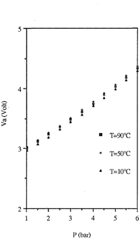
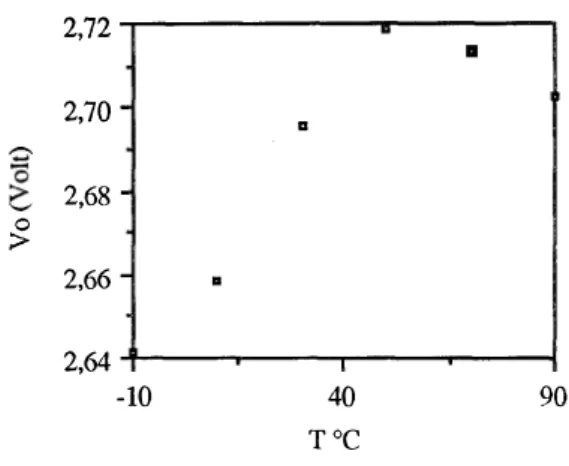
Figures 5 to 7 show the influence of temperature on the responses, the offset voltage and the pressure sensitiYity. Computation of the thermal coefficient of pressure sensitivity yiclds a TCS in the order of 200 ppm/°C. Interestingly, the drifts of Vo and S are
highly com:lateJ. 5---,
.
4-c-i
'ôè
�•
•
T=90°C 3 -1..
T=50°C•
T=l0°C 2 -+---..--.... ,-...---.,----.,----.,-...---1 1 2 3 4 5 6 P (bar)Fig 5: Influence of the temperature on the response
j
!
'-' et:) FiR 6: 0,270 0 0,268- 0.
00,266-.
4 0,264'
·.'
'
-10 15 40 65 T°CPressure sensitivity drift vs. temperature
2,72
•
2,70 • a 2,68 • � 2,66•
2,64 -10 40 90 T°CFig 7: Offset drift vs. temperature
Finally the operation of the mock-up is not disturbed if capacitors less than or equal to 100 pF are connected between the silicon plate and the ground. In our experiments, they simulate parasitic capacitors between the silicon plate and the package or the circuits inputs and the ground. The high value of the parasitic capacitances tolerated by the mock-up suggests that a large variety of packages eau be employed to fabricate sensors.
4 - FUTURE PROSPECTS
The data presented here cannot be considered as fully representative of the mock-up's ultimates potentialities. First it is worth painting out that the temperature range in which the sensor can operate is not limited to -10°C. Indeed, the sensing cell and the
converter eau be opemted down to - 40°C. The actual
limit originales from their mockup packaging that has not been optimized in order to avoid humidity condensation effects. This is a well-known problem that has been adequately addressed by packaging experts.
Also, the rnock-up can be operated al pressures less than 1 bar and higher lhan 6 b:u-s. The pressure causing the plates tu corne into contact is around 20 bars [2]. Consequcntly by propcrly sclccting the capacitances C5 and/or by shifting Vo, the
measurement range can be extended or shifted, and the pressure sensitivity can be increased or decreased.
With respect to nonlinearity errors, the optimization of the form and size of the fixed plates should lead to errors less than or equal to 1 %. Also the temperature influence eau be significantly compensated for by jucliciously varying V dd·
Note that the integmtion of the capacitors Cs into the sensing cell or the converter reduces the total number of devices from four to two. Lastly, the mock-up can be equipped with a self-test fonction by integrating in parallel with Cr and Cm switchable auxiliary capacitors which simulate pressure variations.
REFERENCES
[l] P. Pons, G. Blasquez, R. Behocaray
Sensors and Actuators - A, 37-38 (1993) pp 112-115 Feasibility of capacitive pressure sensor without compensation circuit
[2] X. Chauffleur, G. Blasquez and P. Pons
Eurosensors VIII Conference, Toulouse 25-28 Sept. 1994
Influence of the bonding conditions on the response of capacitive pressure sensors