Universite du Quebec
INRS Energie Materiaux Telecommunications
Multiferroie Materials as Active Elements for
Photovoltaie Deviees
By
Joyprokash Chakrabartty
Memoire Presente Pour l'obtention
du grade de Maitre es sciences (Energy and Materials)
President du jury et examinateur interne
Examinateur externe
Directeur de recherche
(Jury d'evaluation)
Monsieur Andreas Peter Ruediger
INRS Energie Materiaux Telecommunications
Monsieur Pablo Bianucci Concordia University, Canada
Monsieur Federico Rosei
Multiferroie Materials as Active Elements for
Photovoltaie Deviees
By
Joyprokash Chakrabartty
Dissertation
Submitted to INRS-EMT, University of Quebec, in partial fulfillment of the requirements for the degree of
Master of Science in Energy and Materials
Research Supervisor: Federico Rosei, Professor and Director, University of Quebec,
INRS-EMT, Canada
Advisory Committee:
Prof. Federico Rosei, INRS-EMT (supervisor)
Prof. Andreas Peter Ruediger, INRS-EMT (President of the Committee) Prof. Pablo Bianucci, Concordia University (External Member)
Abstract
The discovery ofbulk photovoltaic (BPV) effect in multiferroic (MF) materials has opened
new perspectives in the field of photovoltaics (PV), because the photogenerated charge carriers are separated by an electric field which is not bound to a specific site, or interface. Instead, the mechanism of carrier separation in MFs relies on the electric field created by the spontaneous polarization present in the non-centrosymmetric material. Additionally, when the characteristic dimension of the material is decreased down to nana scale, for example in a multiferroic thin film, the polarization-induced electric field is even more intense. Thus, MF materials eliminate the need for n-p junctions that are usually employed in conventional semiconductor PV devices. However, the electrical power conversion efficiency (PCE) of BPV effect-based devices under sun light illumination is poor, and to date still not comparable with the conventional n-p junction based PV devices. The main reason for this is the low bulk photoconductivity of oxide based MFs, since the BPV originates in the ferroelectric properties, and ferroelectrics are insulating in nature. Therefore, the ultimate challenge in developing competitive devices using the BPV effect is to improve the conductivity by preserving the built-in spontaneous polarization of such type of
material. Nonetheless, the energy band gap of MFs (~1.2-2.7 eV), an important parameter for
photo carrier separation, is smaller than ferroelectric materials (~3-4 eV). Therefore, we
dedicated our work to the development of novel MF materials or heterostructures that would
result in PV devices with competitive PCE.
In first part of our work we developed a multi-stacking scheme, more specifically a
heterostructure based on several BiFe03/BiCr03 (BFO/BCO) epitaxial bilayers grown by pulsed
laser deposition (PLD) onto (100)-oriented LaAI03 (LAO) substrates coated with conductive CaRu03 (CRO) buffer layers. When used as active layers in PV devices, these heterostructures showed a remarkable PCE of -0.01 % when illuminated with 1 sun (AM 1.5G). The fill factor (FF) was determined to be 31 %, a prominent value for both ferroelectric- and MF-based devices. Our results demonstrate that photocurrent density and photovoltage can be tuned by varying the thickness and number of bilayers, opening new perspectives for the design of nov el MF heterostructures with improved PV properties, tuned via engineered interfaciallayers.
In the second part, we focused our efforts to the study of the BPV effect in thin films of Bi-Mn-O material system. The films were again grown by PLD on (111) oriented Niobium doped SrTi03 single crystal substrates. Detailed X-ray diffraction studies show that the films consist of
two main phases, the perovskite BiMn03 (BMO) with a (111)m orientation, and Mn304 phase
having the (101)t orientation. As revealed by <I>-scan measurements, both phases are epitaxially
grown onto substrates. For PV tests we deposited transparent tin doped indium oxide (ITO) top electrodes, and we illuminated the devices using a sun simulator (AM 1.5G). Our findings show that the elemental Bi/Mn ratio in the films controls the magnitude of the photovoltage and photocurrent. Higher Bi/Mn ratio results in an increased PCE, and we obtained a maximum PCE of -0.1 % for the Bi/Mn ratio of 0.82. Film-electrode interfacial effect, modulated by ferroelectric polarization of the film has employed as a model to describe the observed PV phenomena.
Acknowledgement
1 am truly fortunate to have spent more than two years at National Institute for Scientific Research (INRS-EMT), University of Quebec, Canada, that provided me the great opportunity to accomplish my graduate studies in a friendly environment. 1 would like to express my sincere gratitude to Professor Federico Rosei, my supervisor, for aH generous supports he has given me throughout my M.Sc studies.
1 would like to give thanks Dr, Riad N echache, postdoctoral feHow, for spending his valuable time to get me involved in experiments and research very fast. Then 1 would like to take a chance to give thanks to Prof. Andreas Peter Ruediger for his scientific comments on a part of my works. 1 am indebted to aH group members speciaIly Mf. Shun Li and Mf. Daniel Obi, doctoral students, from whom 1 got unconditional supports. Special thanks also go to Dr. Catalin Ramagea for his comments on my dissertation. 1 am also grateful to aIl lab technicians, administrative staffs, and aIl prof essors ofEMT-INRS for their direct and indirect supports.
Last, but not the least, 1 thank my parents who gave me true love and unwavering support during these two years. Therefore, 1 am honored to dedicate my dissertation to my parents.
Table of Contents
Abstract
Acknowledgement ... i
Introduction ... 10
Chapter 1 Properties of Multiferroic Material in Photovoltaics ... 13
1.1 Introduction ... 13
1.2 Magnetism and Ferroelectricity ... 14
1.3 Primary Ferroics ... 15
1.4 Definition of Multiferroic (MF) Material... ... 16
1.5 Photovoltaics with Mutiferroic materials ... 18
1.6 Structure of the thesis ... 22
Chapter 2 Growth Procedure and Characterization Techniques of Thin Films ... 25
2.1 Growth technique ofthin films ... 25
Pulse laser deposition (PLD) oftypical perovskite thin films ... 25
2.2 Characterization Methods ... 28
2.2.1 X-ray Diffraction (XRD) ... 28
2.2.2 Electron Microscopy (EM) ... 30
Scanning Electron Microscopy (SEM) ... 31
Transmission Electron Microscopy (TEM) ... 32
2.2.3 Scanning Probe Microscopy (SPM) ... 33
Atomic Force Microscopy (AFM) ... 34
Piezoresponse Force Microscopy (PFM) ... 35
2.2.4 X-ray Photoemission Spectroscopy (XPS) ... 36
2.2.6 Solar Simulator (AM 1.5) ... 39
2.3 References ... 40
Chapter 3 Photovoltaic Properties of BiFe03/BiCr03 Bilayer Hetero-strueture ... 43
3.1 Introduction ... 43
3.2 Multilayer Films Growth ... 44
3.3 Experimental Results ... 44
3.3.1 Structure and Morphology ... 44
3.3.1.1 XRD Analysis ... 44
3.3.1.2 TEM Analysis ... 45
3.3.2 AFM Study: Surface Analysis ... 47
3.3.3 CUITent Density (J)-Voltage (V) measurement of proposed device geometry ... 48
3.3.4 FeIToelectric Switching of J-V Curve ... 49
3.3.5 Calculation of Power Conversion Efficiency ... 51
3.4 Result and Discussion ... 51
3.5 Conclusion ... 52
3.6 References ... 53
Chapter 4 Photovoltaie Effeet in Multiphase Bi-Mn-O Thin Films ... 55
4.1 Introduction ... 55
4.2 Growth condition and effect ofPLD growth parameters ... 56
4.3 Structure and Morphology ... 57
4.3.1 XRD Analysis: 8-28 and <l> scan measurement ... 57
4.4 Photovoltaic effect: cUITent-voltage (I-V) measurement ... 58
4.5 FeIToelectricity measurement: PFM study ... 59
4.6 X-ray photo spectroscopy (XPS) analysis ... 62
4.7 Optical Absorption: Spectroscopic Ellipsometry Measurement ... 63
4.8 Result and Discussion ... 64
4.9 Conclusion ... 67
4.10 References ... 67
Chapter 5 Conclusion and Future Perspectives ... 71
Table of Figures
Figure 1.1 Schematics ofdifferent types ofmagnetic ordering ... 15
Figure 1.2 Schematic of a hysteresis loop showing coercive field, remnant and saturation strain, polarization and magnetization ... 16
Figure 1.3 Schematics of coupling interactions in multiferroics. 'T' represents torroidal moments
and '0' represents other possibilities of coupling such as spontaneous switchable orbital orderings, vortices, and chiralities ... 17
Figure 1.4 Schematics oftypical structure of the BiFe03 compound ... 18
Figure 1.5 Schematics of the band diagram of conventional n-p junction (a) and band bending of alternative multiferroic photovoltaics (b) ... 19
Figure 1.6 (a) The interfacial effect on the photo voltage in a ferroelectric material showing
depolarized field (Edp) (b) Diagram of metal-film-metal having symmetric and asymmetric
Schottky contacts indicating the interface electric field Ei ... 21
Figure 2.1 Schematic diagram of Pulse Laser Deposition (PLD) ... 26
Figure 2.2 (a) Schematics of diffraction of X-rays by periodic arrangement of planes of atoms (b) example of diffraction pattern obtained for Bi2FeCr06 (BFCO) thin film deposited on (001)
oriented SrTi03 substrate showing the single crystallinity of BFCO ... 29
Figure 2.3 Schematics of a typical Scanning Electron Microscope (SEM) (a) and Transmission Electron Microscope (TEM) (b) ... 33
Figure 2.4 (a) working principle of AFM technique (b) Force- distance curve plotted as a function oftip distance from the sample ... 35
Figure 2.5 (a) and (b) Schematics of changing thickness by applying positive and negative half cycle of ac voltage respectively (c) Schematics of the detection of piezo response signal (d)
x-PFM image of BhFeCr06 epitaxial pattering ... 36
Figure 2.6 Schematic of the principle of Reflection Ellipsometry measurement ... 39
Figure 2.7 (a) Definition of standard spectra and (b) Schematics oftypical spectra ... 40
Figure 3.1 XRD 8-28 scans of BFOIBCO/CRO heteroepitaxial thin films grown on (100)
oriented LAO substrate. x and y in BFO-BCO (x/y) formula represent the thickness (nm) and
number of layer respectively. Squares and stars correspond to K~ and tungsten contamination
contributions, respectively ... 45
Figure 3.2 High resolution TEM images ofheterostructure (a) and (b), with corresponding fast
fourier transform (c), (d), (e) and (f) of each layer individually ... 46
Figure 3.3 EDX spectra of as deposited BFOIBCO/CRO heterostructure. The inset displays the
corresponding low magnification cross-sectional TEM image of the heterostructure ... 47
Figure 3.4 (a) (2 x2 )lm) AFM image of the BCO/CRO/LAO surface and (b) corresponding
surface profile analysis. (c) AFM image of same sample after the deposition of BFO layer. (d)
Schematic representation illustrating the intermixing phenomenon observed during BFOIBCO
characterized by a rough surface and those labeled (2) show the sequential deposition of BFO with the formation of an intermixing zone ... 48
Figure 3.5 (a) Geometry oftested structure involving BFO/BCO bilayers. (b) J-V measurement curves revealing PV effect in BFO/BCO heteroepitaxial films ... 49
Figure 3.6 (a) Evolution of main PV parameters with number of BFO/BCO bilayers (b) PV
properties of the BFO/BCO (15/4) heterostructures after applying pulse bias of ± 15V. The inset
shows z-PFM image (5 x 5 /-lm) with constant applied voltage and variable (± 5V) applied voltage respectively, confirming the switching of ferroelectric polarization ... 50
Figure 3.7 Typical J-V curve under illumination ... 51
Figure 4.1 (a) XRD 8-28 scans of Film A, Film B and Film C grown on (111) oriented Nb: STO substrate shows reflections of (11-1)m orientation of BMO and (101)t orientation of Mn304
phases. Circular and rectangular symbols in (a) indicate (001) Kp lines and tungsten
contamination of x -ray tube source. (b) <Il scan measurements show the three fold symmetry of
BMO and Mn oxide phases in the films ... 58 Figure 4.2 (color on line) J-V characteristic curves of Film A (a) and (b) Film B (d) respectively, with positive and negative poling demonstrating the photovoltaic (PV) effect. The inset in (d) represents a zoom of the J -V curve around origin. The geometry of the tested structure is illustrated in (c) ... 59
Figure 4.3 Voltage vs Polarization curve of Film A & B ... 60
Figure 4.4 F erroelectric hysteresis loops (a, b) and the corresponding CUITent loops (c,d) at different cyc1ing frequencies: while there is a significant leakage contribution, the fact that the switching current dominates at low frequency proves the existence of the ferroelectric component. ... 61
Figure 4.5 piezoresponse force microscopy measurement showing that the as-grown epitaxial BMOlNb:STO(1ll) heterostructure has the polarization oriented downward (bright contrast). (a) surface topography, and (b) PFM image. The regions/grains that do not show a response are either oriented in-plane, or represent the minor MO phase ... 62
Figure 4.6 Deconvoluted XPS spectra of the Mn 2p3/2 peak ... 63
Figure 4.7 (a) Optical absorption coefficient (a) curves as a function of photon energy, measured by Ellipsometry for multiphase Bi-Mn-O thin films. (b) corresponding estimated direct bandgaps ... 64
Figure 4.8 (a) Energy band diagram of isolated ITO, BMO and doped STO (b) Energy band diagram of an ideal BMO/Nb:STO interface at thermal equilibrium (c) Energy band dia gram of ITO/BMO/Nb:STO interface with showing the polarization effect. ... 66
List of Tables
Table 4-1 Phases, compositions and optical properties of BMO films grown on (111)-oriented SrTi03 substrates ... 57
Introduction
The discovery of optoelectronic properties in ferroelectric perovskite thin films has paved the way for the exploration of new approaches for energy conversion including photovoltaic (PV) applications. Without the need for n-p junction, ferroe1ectric polarization of such thin films induces a strong internaI electric field which can be used to separate photo generated charge carriers, thus producing a photovoltage. This effect was named bulk photovoltaic effect (BPV). ln addition to the BPV effect, it has been shown that there is a potential drop across certain types of domain walls in the ferroelectric material, which, for a particular geometry of the domain
structure, results in a total photovoltage (Voc) that exceeds by far the bandgap of the material. [il
The most wide1y investigated multiferroic materials for those applications are BiFe03 (BFO) and Bi2FeCr06 (BFCO). BPV properties have been discovered in numerous ferroelectric materials
such as LiNb03,[2,3[ BaTi0314[ and Pb(Zr,Ti)03.15[ To date, La-doped epitaxial Pb(Zr,Ti)03 thin
films exhibit the highest power conversion efficiency (- 0.005%) under sun light [6[, 10%
external quantum efficiency of BFO 171 and 6% of BFCO [S[ under red light illumination. In
Bi-containing perovskite materials, spontaneous polarization is created by the displacement of Bi
ions, occurring due to the effect of 6s2 lone pair electron.
Due to the coexistence of ferroelectricity and magnetic arder (i.e. transition metal ions with
unpaired d electrons), epitaxial multiferroic films 19,IOJ are interesting materials for PV
applications since they typically have strong unidirectional ferroelectric polarization and smaller
band gaps (typically -1.7-2.7eV) compared to conventional ferroelectric materials (-3.5 eV).
BiMn03 has one of the lowest band gaps, it is reported as the "hydrogen atom" of multiferroic
materials in Ref. [11], and thus it is another promising candidate for PV applications.
However, the external power conversion efficiency of those materials is still po or and also
is under debate. Indeed, the observed photocurrents are insignificant, of the order of nAlcm2,
mainly due to the wide bandgap of ferroelectric (typically 3-4 eV) and their high electrical resistivity. As a result, devices based on ferroelectric films as active layers are not considered promising for PV applications in practice. However, there are two recent reports that changed
the generation of a very high open circuit photo voltages (~15V). A second report, by M. Alexe
and Hesse 1121 demonstrated a drastically enhanced PV effect (up to 30 V photovoltage) from the
single crystal BFO when the top electrode is very sharp. While these two reports apparently contradict each other, one promoting the domain wall PV concept, the other the BPV effect, we believe that they are different facets of a more intricate effect that occurs in these complex materials.
The main objectives of this thesis are to investigate the photovoltaic properties in complex
oxide functional materials. It is expected that when the dimension of these types of materials
go es down to nanoscale (the thickness ofthin films in our case), they show interesting properties compared with their bulk counterpart. The main challenges here are to improve the external power conversion efficiency because multiferroic materials are insulating in nature. Like many others, we tried in this work to improve the efficiency by engineering these types of materials. To do so, we used epitaxial BiFe03, and BiCr03 thin films, periodically multistacked, deposited on a CaRu03 coated LaAI03 perovskite substrate by pulse laser deposition (PLD). Our observation shows remarkable power conversion efficiency and that spontaneous ferroelectric polarization plays a key role in the PV effect. Another part of our work was dedicated to the investigation, of the photovoltaic efficiency of the Bi-Mn-O thin film system deposited on Nb doped SrTi03 perovskite substrate. Ferroelectric polarization modulated film/electrodes interfacial effect has been employed here to explain the observed photovoltaic effect.
References
[1] S. y. Yang, J. Seidel, S. J .Bymes, P. Shafer, c.-H. Yang, M . D .Rossell, J. F. Scott, J. W.
Ager, L.W. Martin, P. Yu, y.-H. Chu, and R. Ramesh, Nature Nanotech. 5, 143 (2010)
[2] A. M. Glass, D. von der Linde, and T. J. Negran, Appl. Phys. Lett. 25, 233 (1974)
[3] A. M. Glass, D. Von der Linde, D. H. Auston, and T. J. Negran, J. Electron. Matter. 4, 915
(1975)
[4] V. M. Fridkin and B. N. Popov, Sov. Phys. Usp. 21, 981 (1978) [5] P. S. Brody and F. Crowne, J. Electron. Matter. 4, 955 (1975)
[6] M. Qin, K. Yao, and Y. C. Liang.Appl. Phys. Lett. 93,122904 (2008)
[7] S. Y. Yang, L. W. Martin,S. J. Byrnes,T. E. Conry,S. R. Basu,D. Paran, L. Reichertz, J. Ihlefeld, C. Adamo,A. Melville,Y.-H. Chu, C.-H. Yang, J. L. Musfeldt,D. G. Schlom, J. W. Ager and R. Ramesh, Appl. Phys. Lett. 95,062909 (2009).
[8] R. Nechache, C. Harnagea, S. Licoccia, E. Traversa, A. Ruediger, A. Pignolet, and F. Rosei Appl. Phys. Lett. 98, 202902 (201 1).
[9] J. Wang et al. Science 299,1719-1722 (2003)
[10] R. Nechache, C. Harnagea, A. Pignolet, F. Normandin, T. Veres, L. -P. Carignan, and D. Ménard, Appl. Phys. Lett. 89, 102902 (2006)
[11] N. A. Hill and K. M. Rabe, Phys. Rev. B 59,8759 (1999). [12] M. Alexe, Nano Letters 12,2193-2198 (2012).
Chapter 1 Properties
of Multiferroic Material in
Photovoltaics
1.1 Introduction
Nanotechnology deals with small struchres or small sized materials. Typical dimensions of interest in nanotechnology are from several subnanometer to several hundred nanometer. A nanometer is one billionth of a meter (lnm :10-e m). For more visualization, one nanometer is approximately the length equivalent to ten hydrogen or five silicon atoms aligned in a row. The idea of nanotechnology first comes from an important talk "There's Plenty of Room at the Bottom: an Invitation to Enter into a New Field of Physics" given by Nobel Laureate Richard Feynman in 1959 at the Califomia Institute of Technology (CalTech) Itl. Since then scientists have been investigating the impact of nanotechnology that can play a vital role in every aspect of society. The term "nanotechnology" was first initiated by Professor Norio Taniguchi of Tokyo Science University in 1974. According to him, "Nano-technology' mainly consists of the processing of separation, consolidation, and deformation of materials by one atom or by one molecule". l'l Later on, the discovery of scanning tunneling microscope (STM) in 1981 opened up an era to see atomic clusters in a material, as a consequence of that, Eigler and E. Schweizer in 1990 from IBM-Almaden Research Centre, Califomia, showed up their ability to arrange individual xenon atoms forming the IBM logo on a single crystal nickel surface using STM tip at low temperatures (4K). Itl
The Physical properties of a material at micrometer scale are mostly the same as that of bulk form, however, decreasing its size in the nanometer raîge, it exhibits distinctively different properties than that of bulk form. Dramatically increased surface area, surface roughness and surface area to volume ratios due to the decreasing material size down to the nanoscale, leads to higher physicochemical properties such as mechanical, electrical, optical, catalylic, and magnetic properties t'1. The.efore, nanotechnology is not only a simple continuation of miniaturization from micrometer down to nanometer scale but also the control of material properties by assembling nanostructures atom by atom or molecule by molecule. Since the field of
nanotechnology is diverse, starting from the study of microstructures of materials to nanostructures to enabling bottom up approach in materials synthesis and fabrication even in terms of biological application, none of them covers the full spectrum of the definition of nanotechnology. In general, nanotechnology is a technology of design, fabrication, and applications with diverse understanding of physical properties and phenomena of nanomaterials and nanostructures. Nonetheless, nanoscience refers to the fundamental study on the relationships between physical properties and phenomena and material dimensions in the nanometer scale. l-'l The most widely accepted def,rnition of nanotechnology in the United States as follows: "concerned with materials and systems whose structures and components exhibit novel and significantly improved physical, chemical and biological properties, phenomena and processes due to their nanoscale size". Iul Thin films, nanowire, quantum dots are examples of the most widely investigated nanostructured materials now a days.
1.2 Magnetism and Ferroelectricity
The magnetism in a material lies in the orbital and spin motions of electrons and the way of interaction of electrons with one another. Whether a material is magnetic or not, depends on the response of that material under applying magnetic fields. Most materials are magnetic in a sense but some of them show higher magnetism than others. The main reason of showing this difference is that there is no collective interaction of atomic magnetic moments in some materials, whereas in other materials there is a very strong interaction between atomic moments. The magnetic behavior of materials is classified as follows: i) diamagnetism ii) paramagnetism iii) ferromagnetism iv) ferrimagnetism and v) antiferromagnetism. The distinction between the different types of magnetism lies on the collective magnetic interactions and ordering of the magnetic entities present in the material. Figure 1.1 shows different types of magnetic ordering based on such type ofinteraction and ordering.
r r ù a A r ' f l i i ù f t $ t t È r f l
J u
*.\ t
/ \ \\ , 1 , /
r F,ff" | !llr,'t fl 11f I * 6r',1i + + + + + + + + f *r'1.ûûrÈfln* t'l*'?t1 4 + + àn t l -l*rr,f,rrÉgnIi I em -+ + ÊFigure 1.1 Schematics of different types of magnetic ordering [7]
A crystal is said to be ferroelectric when it possesses at least two equilibrium orientations of the spontaneous polarization vector in the absence of an external electric field, and the spontaneous polarization can be switched between those orientations by an electric field lsl.The distinct characteristic of a ferroelectric is the spontaneous polarization (P), which is a reversible polar vector. It develops as a result of a symmetry reducing phase transformation that displaces positive and negative charges along a restricted family of crystallographic directions, resulting in a pennanent electric dipole moment lel. To be ferroelectric, this dipole moment must have two or more crystallographic equivalent directions. Ferroelectricity was first discovered by Valasek in
7921rnRochelle salt.
1.3 Primary Ferroics
A ferroic is a material that exhibits spontaneous and switchable intemal alignment by an external stimulus. The primary, well established types of ferroic materials are ferroelectric, ferromagnetic and ferroelastic shows spontaneous electric polarization, spontaneous magnetisation and spontaneous strain. The alignment of electric dipole moment in ferroelectrics, alignment of electron spins in ferromagnetics and strain alignment in ferroelastics can be switched by their conjugate quantities, i.e. the electric, magnetic and strain field, respectively [r0l. In general, ferroic materials exhibit a hysteretic behavior when the extemal driving force is cycled, as shown in Figure 1.2.
I\I,, T,, P,
Figure 1.2 Schematic of a hysteresis loop showing coercive field, remnant and saturation strain, polarization and magnetization [1 ll.
1.4 Definition of Multiferroic (MF) Material
Any materi al that exhibits more than one primary ferroic ordering in the same phase lr2l is called multiferroic. A particularly important class of multiferroics is that which comprises ferro-electricity and one type of magnetic order in the same phase. It covers not only ferroic ordering but also anti-ferroic ordering. For an example, BiFeO3 most widely investigated multiferroic compound, exhibits both fenoelectricity and anti-ferromagnetism at room temperature.
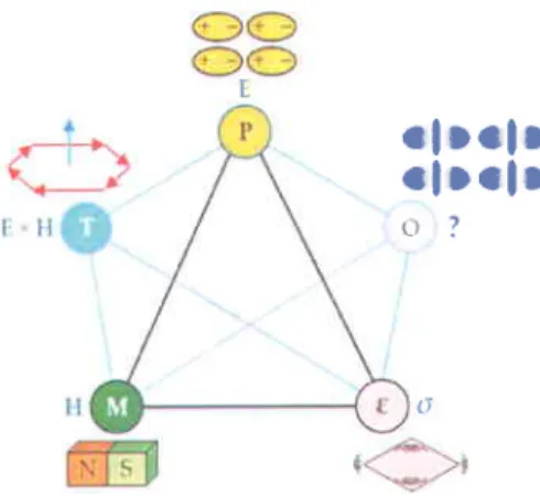
Mutiferroics can be classified into two groups: materials with independently originating ferroelectricity and magnetism, and materials in which magnetism causes ferroelectricity. The second group brings one of the most appealing aspects of multiferroic material and is referred to as 'magnetoelectric (ME) multiferroics". The interdependence of the relevant quantities in such a material is shown in Figure 1.3 that extends its application into spintronic.
l
. f D e f D
r f l c l o
o ?
( l
Figure 1.3 Schematics of coupling interactions in multiferroics.'T'represents torroidal moments and 'O' represents other possibilities of coupling such as spontaneous switchable orbital orderings, vortices, and chiralities [10].
From the crystallographic structural point of view, multiferroic materials are divided into four classes: perovskite oxides e.g. BiFeO3, TbMnOr; hexagonal oxides e.g. RMnO3 where R: Ho, Er, Tm, Yb, Lu, as well as Y and Sc; boracites e.g. MlBzOr:X where M is a bivalent metal ion (M: Cr, Mn, Fe, Co, Cu, Ni) and X:Cl, Br, I; and BaMF+ compounds where M: Mg, Mn, Fe, Co, Ni, Zntttl. In our work, however, we focus on the perovskite structure, more specifically on the complex oxide perovskites because of its good ferroelectricity, large dielectric constants, ferromagnetism, and antiferromagnetism Iral. Most of the perovskites fall into this complex oxide group because it comprises two or more transition metal cations (typically 3d) with oxygen. In addition, oxides are abundant compounds on earth. The general chemical formula of the perovskite structure used in this work is ABXI, or AzBB/Xo (for the double perovskite) where 'A' denotes nonmagnetic cation and 'B' denotes magnetic cation. Figure 1.4 shows the typical perovskite unit cell of bismuth ferrite, BiFeO: (BFO). The rhombohedrally distorted perovskite BFO exhibits a prominent spontaneous polarization (-100 pClcm2 at room temperature; Its' t0l below the fenoelectric transition temperature (26': 1,103 K) giving antiferromagnetism below the antiferromagnetism Neel temperature (TN:643K).
[ 1 1 1 1
Figurc 1.4 Schematics of typical structure of the BiFeO3 compound [17]
In conventional ferroelectric materials, ferroelectricity originates from the non centrosymmetric nonmagnetic cation that shifts away from the center of the surrounding anions. The noncentro-symmetricity between positive and negative charges gives rise to the electric dipole moment. In contrast, in a magnetic material, the magnetic cation (having apartially filed d orbital) tends to sit exactly at the center of the surrounding anions, i.e the centrosymmtric position is favored, resulting in no dipole moment. Since both ferroelectricity and magnetism do coexist in the multiferroic material, it means there is a competition between the formation of energy-lowering covalent bond and the energy-raising electronic coulomb repulsion t8l. The compromise between them makes off-centering of the A site cation, Bi3* in the case of BFO, to result in the apparition of a dipole moment, thus ferroelectric behavior. In other words, fenoelectricity can also generate from the structural instability which is compatible with the coexistence of magnetism ll{t' le' 201.
1.5 Photovoltaics with Mutiferroic materials
In conventional n-p junction based PV devices, the photo generated charge carriers are driven by the electric field l2rl created at depletion region. This means that the open circuit voltage (Vo.) in this case is limited by the band gap of the material, normally less than the band gap (eVo" a Eg). In contrast, in the case of the photovoltaic effect in ferroelectrics, the photo
generated electrons and holes are further separated by the internal electric field present in ferroelectric materials, which originates from the inbuilt spontaneous polarization I2:1. The basic difference between these two types of PV devices lies in the magnitude and the range of their carrier driving force i. e. the electric field. Polarization-dependent electric field (i. e. depolarization field, Epp) in the ferroelectric material is at least an order of magnitude higher than in conventional n-p junction based devices. In addition, the depolaization field is not confined in a small zone as is the case of the p-n interface. Similar to the n-p junction, lower band gap MFs possess ferroelectric behavior that develops electric freld in the whole volume of the material, a critical issue for photo charge carrier separation in PV devices. The mechanism of photovoltaic effect in MFs can be explained in similar fashion of p-n junction, shown in Figure 1.5. Here in the case of BFO thin film with a particular domain wall, the changes of abrupt polarization are occuffed at the domain wall. This imbalance of charges l2'rl creates an electrostatic potential drop (typically between 0.02-0.2 eV) across the domain wall which is responsible for band bending in this region l2rl. Note that the domain wall is much thinner (2 nm) than the depletion layer of a n-p junction, therefore, charge separation is much more effective and faster.
Figure 1.5 Schematics of the band diagram of conventional n-p junction (a) and band bending of alternative multiferroi c photovoltaic s (b). Adapted from refere nce - [2 4]
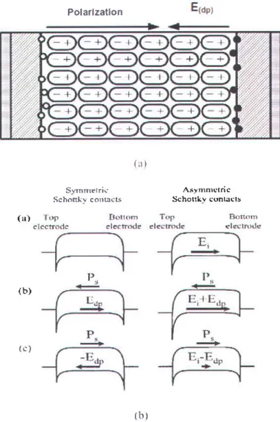
For thin film solar cells based on MFs, electrodes are also required to contact with the films that creates Schottky contact at film-electrode interface. Therefore, the photo charge carrier
driven total intemal electric field is the combination of two components: (i) the depolarization freld (E6o) originating from the polarization alignment in the bulk of the film, and (ii) the net interface electrical field (E) resulting from the electrode-film interface. As illustrated in Figure [.6, the depolarization field (E6o) originates from spontaneous polarization and opposite to the direction of polarization, and the interface electric field (E) is polarization independent, and it orisinates from the Schottky contacts of the electrode-film interface.
Polarlzatlon Siymnrrtric Schonliv co|rt!{ts { i t l A.*y nrnrçtric Schortkv l;unlilcls ( , J ) ( l ' r l
Figure 1.6 (a) The interfacial effect on the photo voltage in a ferroelectric material showing depolarized field (E6o) t25l (b) Diagram of metal-film-metal having symmetric and asymmetric Schottky contacts indicating the interface electric field Et [261
However, power conversion efficiency of devices based on MFs is still poor due to the intrinsically low bulk conductivity, compared with that of a commercially available silicon based solar cell. This is explained as follows: for fenoelectricity to exist in a multiferroic material it must be insulator in nature, otherwise the mobile charges will screen out the electric polarization lt7l. In fac|, any efforls to rise up conductivity of ferroelectrics result in a lower spontaneous
( n )
t b )
polarization, and as a consequence, lower internal electric field. Since the latter is directly related with the separation of photo generated charge carriers, this results in lower power conversion efficiency. However, efficient synthesis of nano structure and material engineering could be an effective way of improving PV efficiency.
1.6 Structure of the thesis
Chapter 2 describes shortly the main experimental methods used throughout this works. Starting with the pulsed laser deposition technique (PLD), a prominent tool for complex oxide film growth, the effect of several key parameters on the quality of thin films is discussed. Then the chapter covers the different types of thin film characterization methods that have been used to analyze the result in this thesis. For example, X-ray diffraction (XRD) and Transmission electron microscopy (TEM) was used to analyze structure and morphology of as-deposited thin film. Atomic force microscopy (AFM) and Scanning electron microscopy (SEM) was used to visualize the surface topography and Piezoresponse force microscopy (PFM) proved the presence of ferroelectricity in thin f,rlm. Optical absorption and band gap were measured by spectroscopy ellipsometry. Finally, the experiments using a solar simulator are explained in short as they give the value of the photocurrent and the photovoltage, which are the basis for calculating the power conversion efficiency. Chapter 3 presents the experimental results of PV efficiency obtained on BiFeO3/BiCrO3 bilayer thin film deposited on LaAlO3 substrates. The key finding is the dependence of photo current and photo voltage on number of bilayer incotporated in the structure. Thickness dependent absorption depth (Beer-Lambert Law) had been employed to explain the nature of observed photovoltage and photocurrent because of closer band gap of BFO and BCO layer. In Chapter 4, we report the photovoltaic effect in BMO thin films, a result that has never been reported before. We present a comparative study of the photovoltaic efficiency of three Bi-Mn-O thin films with different compositional ratios Bi:Mn, deposited on (111) oriented Nb doped STO perovskite substrates. Higher Bi/Mn ratio exhibits higher PCE. The observed PV phenomena are explained by the combined effect of ferroelectric polarization and film/electrodes interfacial. Chapter 5 concludes the thesis with a summary of our findings and future perspectives.
1.7 References
[] Richard P. Feynman, Caltech Engineering and Science, Volume 23:5, pp 22-36, February 1 9 6 0
[2] N. Taniguchi, Proc. of International Conference on Precision Engineering (ICPE), Tokyo, Japan, pp.18-23,1974
[3] D. M. Eigler and E. K. Schweizer, "Positioning single atoms with a scanning tunnelling microscope" Nature 344, 524 (1990)
[4] B. D. Fahlman, Materials Chemistry, Springer, Dordrecht, Netherlands,2007
t5l Guozhong Cao (University of Washington, USA) and Ying Wang (Louisiana State University, USA), Nanostructures and Nanomaterials - Synthesis, Properties and Applications (2nd Edition) @ World Scientific Publishing Co. Pte. Ltd.
[6] National Nanotechnology Initiative 2000 Leading to the Next Industrial Revolution, A Report by the Interagency Working Group on Nanoscience, Engineering and Technology (Washington DC: Committee on Technology, National Science and Technology Council), http://www/nano.gov
lTlhttp:llwww.rug.nl/researcUzemike/education/topmasternanoscience/nsl90khikhlovskyi.pdf [8] Lines and Glass, Ferroelectrics and related materials, Oxford (1977)
f 9l http://scholar.lib.vt.edu/theses/available/etd-08062008- l02S5T ltnrestricted/Dissertation2.pdf [10] N. A. Spaldin, S. W. Cheong, and R. Ramesh, Physics Today, P-38, October 2010
[11] Naigang Wang, M.Sc thesis, Material Science and Engineering, Virginia Polytechnic Institute and State University, 2005
[12] H. Schmid, Ferroelectrics, 162, 317 (1994)
[13] G. A. Smolenskii, I. E. Chupis, Ferroelectric magnetic materials, Usp. Fiz. Nauk 137, 415-448 (1982) (in Russian)
U4] Y. Tokura, Colossal Magnetorestive Oxides, Gordon and Breach Science Publishers, Amsterdam, Netherlands, 2000
[15] J. Wang, J. B. Neaton, H. Zheng, V. Nagarajan, S. B. Ogale, B. Liu, D. Viehland, V. Vaithyanathan, D. G. Schlom, U. V. Waghmare, N. A. Spaldin, K. M. Rabe, M, Wuttig, R. Ramesh, 299, 1719-1722, Science 2003
[16] K. Yun, D, Ricinschi, T. Kanashima, M. Noda, M. Okuyama, Jpn. J. Appl. Phys. 2004,43, L647-L648
|Tlhttp:llcdn.intechopen .comlpdfsl44g29llnTech-Optical,properties_of multiferroic_bifeo3_films.pdf [18] B. B. van Aken, T. T. M. Palstra, A. Filippetti, & N. A. Spaldin, Nature Mater. 3,164-170 (2004)
[19] C. J Fennie, K. M. Rabe, Phys. Rev. B 72, 100103(R) (2005) l20lC. Ederer, N. A. Spaldin, Phys. Rev. B 74,I (2006)
[21] S. M. Sze, Physics of Semiconductor Devices, 2nd edn (John Willey & Sons), 1981 l22lMengQuin, Kui Yao, Yung C. liang, Appl. Phys. Lett.93,122904,2008
[23] S. Y. Yang, et al. Nature Nanotech 5,143-147 (2010) l24lHaitao Huang, Nature photonics, vol4, March 2010
t25l Q. Meng, Y. Kui, and C. L. Yung, Applied Physics Letters, 93 (12), p.122904 (2008)
l26lY. S. Yang, S. J. Lee, S. Yi, B. G. Chae, S.H.Lee, H. J. Joo, M. S. Jang, AppliedPhysics Letters, 76 (6),p.774-776. (2000)
Chapter 2 Growth Procedure and Characterization
Techniques
of Thin Films
2.1 Growth technique of thin films
Pulse laser deposition (PLD) of typical perovskite thin films
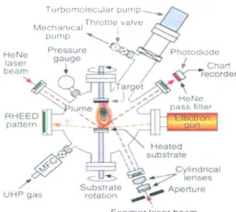
Pulsed laser deposition (PLD) is a physical vapor deposition process which shares some process characteristics with molecular beam epitaxy (MBE) and some with sputtering deposition. A PLD system consists of a closed high vacuum chamber equipped with the facilities needed for rotating atarget containing the material(s) to be deposited, in front of the substrate, on which the film is grown. The physics behind laser-matter interaction, starting from creation of plasma plume to plasma expansion has been described well in reference ['1. A tlpical PLD system is shown in Figure 2.1. A pulsed laser beam with sufficiently high energy density is focused on the surface of the target material. Each laser pulse ablates a small amount of material from the target, creating a plasma plume in front of the surface. The plume expands adiabatically towards the substrate, where the material is deposited. Generating and expanding plasma plume undergoes three consecutive processes: interaction of the laser beam with the target material resulting in evaporation of a thin surface layer, interaction of the evaporated material with the incident laser beam resulting in an isothermal plasma formation and expansion, and anisotropic adiabatic expansion of the plasma leading to the characteristic nature of the laser deposition process lrl. This plume supplies sufficient material to the substrate for frlm growth. The successful sl.nthesis by PLD of perovskite structured complex oxide material (more specif,rcally high temperature super conductors) has been achieved in the late 1986, and started a new era in film growth techniques. PLD has several characteristics that make it competitive in complex oxide thin frlm research area as compared to other film growth techniques. The most important advantages of PLD are the stoichiometric transfer of the ablated material from multicomponent target, excited oxidizing species l2l, and the simplicity of its set up. Due to these attractive characteristics as a multicomponent film growth technique, a number of applications have been actively pursued for the fabrication of specific structures and devices. Now a day PLD has been widely used in depositing insulators, semiconductors, metals, poll.rners, and even soft biological materials.
ïurbonrolecutar Êunrp *_r, M e c h ê n r c â l T h r # l l l e v a l v e p{rmp ---__f
{hbr
P h ( ) t o c i r o d e I r:^.* - i {. xbr'ro Ë a s s f i l t e rExçrrn*r laser beanr
Figure 2.1 Schematic diagram of Pulse Laser Deposition (PLD) [31
In PLD, there are several parameters that might affect the morphology and crystal quality of thin film. The most fundamental parameters are the vacuum base pressure (-10-5-10-10 mbar), the background gas pressure (for most complex oxide materials -1-100 mbar), substrate temperature during deposition (500-10000C), laser fluence (I-3 Jlcmz for most perovskite oxide materials), laser frequency (repetition rate of the pulses, l-20H2), the distance between the target material and substrate distance, and laser spot size on the target material. Each and every parameter is interdependent. Changing one parameter affects the deposition ratelgrowth rate (0.001 to I A0) of the thin film resulting in changing the morphology. On the other hand, there are some other consideration to investigate penetration of growth and film quality that is directly related with the substrate, such as orientation and crystalinity, lattice constant, and whether the surface is singular or vicinal. Depending on the surface free energy of the substrate, three classical growth modes can be distinguished: Frank Van der Merwe, Volmer-Weber and Stranski-Krastanov lal. Apart from that there are another four epitaxial growth modes that is often used such as step flow mode, columnar growth, step bunching, and screw-island growth.
A particular importance in PLD has the background gas in the chamber at the time of deposition, because it affects the phase formation of the multication system. In complex oxide materials, for example in the case of BiFeOl film deposition, the background oxygen pressure serves as a reactive species for plasma plume to form the appropriate phase on the substrate,
depending on the thermodynamic stability of that phase. Besides, the background gas reduces the kinetic energy of the species in the plume. This kinetic energy has an important impact on the substrate deformation since high energetic species introduce compressive stress. The compressive stress associated with subsurface damage from the impinging energetic species leads to interstitial defects and thus a lower quality of the resulting film.
It is also crucial to maintain the substrate at the optimum deposition temperature in order to achieve the appropriate phase formation, a condition generally required for any material grown by PLD. A low deposition temperature usually prevents the formation of the crystalline phase of the film. Nonetheless, a deposition temperature above optimum causes inter-diffusion reaction at the interface between film and substrate, or the reconstruction of the substrate surface that strongly alters the physical properties of the as grown films. For instance, if the temperature at the time of deposition of Bi based perovskites is too high, re-evaporation of volatile Bi components from the film occurs, resulting in a film with Bi deficiency. In a nutshell, the kinetics of film growth is partially dependent on the selection of proper temperature.
One of the most important drawbacks of PLD is the formation of micron size particles, called droplets, on the film surface. Droplets are transferred to the substrate when the penetration depth of the laser pulse into the target material is large enough. The use of highly dense target material might reduce droplets but not completely. Therefore, some sort of mechanical techniques have been employed to reduce the droplets, specifically velocity filters, off-axis deposition and line of sight shadow masks ls' 6' 71. Thickness uniformity of the film when depositing over a large area is another critical challenge of the PLD technique. The highly directional nature of the ablation plume hinders the growth of films with uniform thickness over large area. Recent developments in the design of the PLD system, however, minimize this problem by employing raster scanning of the laser beam over the surface of the target and rotating the substrate.
In this study, we have used a fully equipped PLD system consisting of a GSI Lumonics KrF excimer Laser (1,:248nm with a pulse FWHM t:15.4 ns) and a vacuum chamber. The chamber is evacuated to reach our required background vacuum pressure (-10t mbar) by using a mechanical and turbo pump establishing outside of the chamber. The train of laser pulses enters
into an optical system made of mirrors and lenses, then enters the chamber through a qvartz window and strikes the target material at an angle of 450 from the surface normal. The laser beam is focused such that the impact region (the "laser spot") has the desired size, thus controlling the incident energy density.
A numerical computer control system has been employed to control and measure the laser parameters particularly pulse repetition rate, laser energy and number of laser pulses. The substrate temperature is monitored using a K-type thermocouple during film deposition. The typical deposition temperature was between 5800 C and 8600 C depending on requirement. Substrate-target distance has been controlled manually and it was kept constant at 5.5 cm. The calculated laser fluence was in between | - 4 Jlcmz and laser repetition rate was between of 2-8 Hz.
2.2 Char acterization
Methods
2.2.1 X-ray Diffraction (XRD)
The discovery of X-rays in 1985 by German physicist William Roentgen was the breakthrough of many aspects of science. The immediate application of the X-rays was radiography-widely used nowaday in medical science by physicians. Later on Von Laue et al. in 1912 showed atomic diffraction patterns of crystalline material (zinc sulfide) by X-rays followed in l9l4 by English physicist Sir William Henry Bragg and his son Sir William Lawrence Bragg who showed that the scattering of x-rays could be as "reflection" by successive planes of atoms within a crystal. With the arrival of monochromatic X-ray sources, it has further been shown that a periodic arrangement of atoms in a crystal leads to the diffraction of X-rays. The intensity of the diffracted wave might be maximum or minimum depending on the type of interference. Constructive interference of scattered photons leads to high intensity.
+ t d -' E
s
\ ir. î t { J t :_o 1/ri-dr{sf ù r , ' s (a) . , f * ''t r ' r j j u r r .'" " ' $ u ' f t r f \ l t $ $ln ll r r t a l f, " r . , ?d trn lf C 0r151rLgl'w lnlsf lixsrKs vrnûfl n À = 2 d s i n 0 Eragg's Law a a t a t fFigure 2,2 (a) Schematics of diffraction of X-rays by periodic affangement of planes of atoms l8l (b) example of diffraction pattern obtained for BizFeCrO6 (BFCO) thin film deposited on (001) oriented SrTiOr substrate showing the single crystallinity of BFCO [9]
This is shown clearly in Figure 2.2 (a) which illustrates the working principle of XRD. Geometrically, the distance between two parallel planes of periodically arranged planes (d),the wavelength of a monochromatic X-ray source (,1) and the diffraction angle (0) are being correlated with each other by the following equation known as Bragg's law, n7:2dsin0,where n is the order of reflection. Since the wavelength (2) is about equal to the distance between two atoms (approx. 0-5 A0), the XRD technique is an extremely powerful tool for measuring crystalline structure of a given material.
The experimental setup for performing an XRD experiment is very simple in nature. A beam of X-rays from a monochromatic X-ray source is focused on the sample, under a precise incident angle. This sample is fixed on the movable flat plate. The diffracted beam from the sample is then collected in an X-ray detector, which gives a signal proportional to the number of photons along the sample-detector direction. This signal is then recorded as a function of 20 (see Fig. 2.2). Each parallel set of crystalline planes of the investigated sample produce an unique diffracted pattern. This pattem is then compared with a library of standard patterns (in X'Pert High Score) of specific structure of elements as well as compounds. Finally, a set of information about such as crystalline structure, crystallite size distribution, and lattice parameter has been extracted by analyzing angular the position of the recorded diffracted peak maximum, amplitude and width of the peak. Figur e 2.2 (b) shows an example of typical XRD data.
We used a high quality XRD system, namely the High resolution PANalyticalX'Pert Pro MRD 4-circle diffractometer system. This system gives us facilities to do a lot of measurements
J O a ô r ô d '
I'hctr/2l"h.rr r(- I
rrt'('() t ,
l ' l l l r \
such as phase analysis in 0-20 (Bragg-Brentano), grazing incidence, Phi scan measurement to test the epitaxial deposition, texture analysis, high resolution reciprocal space mapping, high resolution rocking curve measurement, residual stress analysis and X-ray reflectivity measurement. In our study, we used extensively 0-20 and grazing incidence measurement to realize the strucfure and quality of the as-deposited thin frlms. ln addition, using X-ray reflectivity measurements we assessed the thickness of the as-prepared films.
2.2.2
Electron Microscopy
(EM)
Conventional light microscopy (LM) uses visible light of wavelengths from about 400 nm to 700 nm with a resolution of 0.2 microns (p) as a source of illumination and optical lenses to magnify the sample. In contrast, electron microscopy (EM) uses a high energetic focused electron beam in a vacuum to investigate an object on a very f,tne scale. The advantage ofEM over light microscopy consists in the very short wavelength associated to electrons (À:0.005nm at an accelerating voltage of 50KV) with a resolution of about 25 angstrom (R0) that, in principle, enables atomic scale resolution. It uses electromagnetic lenses to magnify the specimen. EM yields information about the topography (surface features of an object), morphology (shape and size of the particles making up the object), composition (the elements and compounds that the object is composed of and the relative amounts of them) and crystallographic information (how the atoms are arranged in the object) Ir0l.
The basic research on electron microscopy has been started in 1920's when the properties of accelerated electrons (wavelike properlies with shorter wavelength than visible light) in vacuum have been discovered. As a consequence of the progress of research, in 1931, Max Knoll and Emst Ruska constructed a two stage electron microscope with three magnetic lenses, condenser, objective, and projecto. [ttl, known as the first Transmission Electron Microscope (TEM). Later on in 1938, Manfred von Ardenne invented another type of electron microscopy based on the scanning of an electron beam over a sample and they called their system scanning electron microscope (SnV; ttzt.
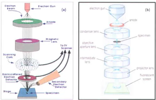
An electron microscope consists of an electron optical column, a vacuum system, electronics and software. All these function together obtains a good image of specimen. In principle, when a sample is bombarded with an incident electron beam, there might occur two
types of collisions: elastic and inelastic, which produce backscattered electrons, secondary electrons, Auger electrons, characteristic X-rays and cathodoluminescence. Based on these emitted electrons, two basic tlpes of electron microscopes exist, namely Scanning electron microscope (SEM) and Transmission electron microscope (TEM) that are briefly explained below.
Scanning
Electron Microscopy
(SEM)
Scanning electron microscopy (SEM) uses a focused electron beam that rasters over the surface of the sample in vacuum to extract structural and chemical information point-by-point from a region of interest in the sample. The high spatial resolution of an SEM makes it a powerful tool to characteize a wide range of specimens at the nanometer to micrometer length scaleslt'|. Scan coils and objective lens shown in Figure 2,3 (a) are used to deflect the electron beam horizontally and vertically in order to achieve a proper scanning over the surface of the specimen. Based on the type of electron scattering, a reasonable amount of emitted electrons is collected by appropriate detectors. The output of these detectors is synchronized with the x-y input of the cathode ray tube (CRT) where images are formed, according to the x-y beam deflection on the surface. The following equation denotes linear magnification, M:L/I, where 'L' is the scanning length of the CRT monitor and 'l' the scanning length on the surface of the specimen.
The typical beam diameter of the SEM is between 5 nm to 2pm and the working (accelerating) voltage is from 2 to 50 KV. SEM deals with basically three types of signals: secondary electrons, backscattered electrons, and elemental electrons. In SEM, secondary and backscattered electron signals are used for the visualization of the surface of a specimen. Secondary electrons, a result of inelastic collisions, are used to image the surface structure of a sample with the resolution of 10 nm or better. Nevertheless, backscattered electrons, a result of elastic collision, help to resolve topographical contrast and atomic number contrast with a lateral resolution better than 1 micron. While secondary electron imaging infers energy of the emitted electrons below 50 eV, the backscattered electrons have an energy greater than 50 eV llal. The limitations of SEM are that it can only deal with conductive specimens and gives only surface
image. In addition, it cannot detect those materials which have atomic number smaller than that ofcarbon.
Transmission
Electron Microscopy (TEM)
When a beam of electrons passes through a crystalline specimen, it is scattered according to the Bragg's law. The scattered beams at small angles are focused by the objective lens to form a diffraction pattem at its back focal plane. The scattered beams are recombined to form an image in the image plane ltst. Figure 2.3 (b) shows a typical schematic of a TEM. In the case of diffraction patterns, the whole illuminated area of sample generates electrons, and, in order to protect the screen, a virtual image of the specimen is produced by placing a small aperture in the image plane of the objective lens. The pattern obtained by placing this aperture is called selected area diffraction (SAD). TEM gives two types of imaging of a sample, depending on whether direct electron transmission or scattered electrons are involved. If the directly transmitted electron beam is used, the image obtained is referred to as the bright-field image, while the scattered electron beam results in the so-called dark-field imaging.
TEM provides information about the crystalline structure of the specimen by showing different types of diffraction pattems such as dots, regions or circles that originate from the irradiated area of the sample. Dotted, center-circled and diffuse-circled diffraction pattern indicates mono-crystalline, polycrystalline and amorphous structure of the specimen, respectively.
tlælrtr 3.ffi I f l a c t r s G u n F ( a ) M ognalrc . t s t 6 { b )
Figure 2.3 Schematics of a typical Scanning Electron Microscope (SEM) (a) I10l and Transmission Electron Microscope (TEM) (b) Il0l
2.2.3 Scanning
Probe Microscopy
(SPM)
The probe-based microscopies, referred to as SPMs, have been developed since the discovery of Scanning Tunneling Microscopy (STM) and Atomic Force Microscopy (AFM) in
1982 by Gerd Binning and H. Rohrer, and 1985 by Binning et al respectively. SPMs allow investigation and manipulation of a specimen surface down to the atomic scale and thus it is associated with nanoscale science and technology. SPMs enable sharp imaging of sample surface by means of measure a local physical quantity related to the interaction between a sharp probe (tip) and the surface of the sample. Dedicated software and electronics process all the extracted data in order to render an image of the surface of the specimen. Due to their astounding capability to probe tip-sample interactions, SPMs have become of increasing interest for imaging electronic, magnetic, biological, and chemical properties at the surface of various specimens. In our wotk, we used two basic scanning probe microscopes, named atomic force microscopy (AFM) and piezoresponse force microscopy (PFM). They are briefly discussed below.
Atomic Force Microscopy (AFM)
The fundamental working principle of AFM relies on the measurement of the forces between a sharp fine tip and a sample. The tip is typically attached to the free end of a flexible cantilever and is brought in the proximity of the sample surface. The force acting on the tip is transmitted to the cantilever, which deflects a laser beam reflected off from its back onto a segmented photodiode that gives signals which can be used to obtain the deflection of cantilever. Therefore, the interaction force can be monitored/controlled, and, by doing this while the tip is rastered across the surface, the sample topography can be retrieved. Figure 2.4 (a) shows the schematics of the general working procedure of all SPMs.
There are three modes of operation of an AFM: contact mode, non-contact mode and tapping mode (intermittent contact mode). Figure 2.4 (b) shows a force vs distance curve indicating the three modes of operation. In contact mode operation, the tip makes a soft physical contact with the sample while scans over the sample by maintaining either a constant small height (less than a few angstrom) or under a constant force (van der Waals force, capillary force and force extracted by the cantilever itself). It yields atomic scale of resolution with high scan speed but might distort the image because of lateral force of cantilever. In non-contact mode, the tip scans while maintaining a sufficient distance (approximately at least one nanometer) from the sample surface and operates in the attractive force region of the figure. This mode prevents breakage of soft sample but yields lower lateral resolution due to tip-sample separation. In tapping mode, the cantilever oscillates close to its resonance frequency and the tip touches the scanning surface only for a fraction of its oscillation period. An electronic feedback loop ensures a constant oscillation amplitude by adjusting the tip-sample separation. Despite of its slower scan speed, tapping mode operation presents high lateral resolution (lnm to 5 nm) of the tested sample.
t!!itk'
Figure 2.a @) working principle of AFM technique (b) Force- distance curve plotted as a function of tip distance from the sample [16]
In our work, we have used AFM measurements to characterize the surface of the as-grown films using Veeco Dl-EnviroScope microscope. Tapping mode operation of AFM has been selected to make an image of surface topography.
Piezoresponse
Force Microscopy
(PFM)
PFM is a versatile tool for the detection and imaging of ferroelectric domains at nanoscale, based on the converse ferroelectric effect. In PFM, the signal originates in the deformation of the ferroelectric material upon applying a small electric field. Figure 2.5 shows a typical PFM image and explains the imaging principle of PFM, where an applied alternating voltage on the conductive AFM tip creates an electric field in the sample. Depending on the parallel or perpendicular direction of polaization with respect to this electric field, PFM detects and creates an image of either out of plane (z-PFM) or in plane (x-PFM) polarization, respectively.
Extracting the induced sample oscillations of the sample surface is a complex process. To do it, a lock-in system is employed that eliminates the noise together with all harmonic components from the actual deflection signal. The remaining signal thus represents only the sample response, and is referred to as piezo response signal.
{ a )
(bt
( c ) { d }
Figure 2.5 (a) and (b) Schematics of changing thickness by applying positive and negative half cycle of ac voltage respectively [16] (c) Schematics of the detection of piezo response signal [16] (d) x-PFM image of BizFeCrO6 epitaxial pattering [17]
In our experiment, we used the same commercially available instrument, the Veeco DI-Enviroscope, equipped with a computer controlled lock-in amplifier (Signal Recovery model 7265). In this instrument, the cantilever axis is contained in the plane of the laser beam. A conductive silicon cantilever coated with Co-Cr (NSC 36lco-Cr) was used for applyng the AC voltage. The silicon cantilever is highly doped, and its resonance frequency and spring constant are 68.68 KHz and 0.5 N/m, respectively. The amplitude of the applied AC voltage was in the range from 0.5V to lV. Hysteresis loop measurements were performed using a computer controlled Keithley 2400 Digital SourceMeter (Cleveland, OH) which supplied the DC voltage (-5V to +5V), connected in series with the AC source.
2.2.4
X-ray Photoemission
Spectroscopy
(XPS)
X-ray photoelectron spectroscopy (XPS), also known as electron spectroscopy for chemical analysis (ESCA), is one of a number of surface analytical techniques that bombard the sample with photons, electrons or ions in order to excite the emission of photons, electrons or ions lttl. In
XPS, the sample is irradiated with low-energy (-1.5 keV) X-rays and measures energy spectrum of the emitted photoelectrons to obtain quantitative analysis of the surface by means of a high-resolution electron spectrometer. The high resolution beta ray XPS was developed in 1960s by the several significant improvements in the equipment by the group of K. M. Siegbahn. In recognition of his extensive efforts to develop XPS into a useful surface analytical tool, Siegbahn was awarded half of the Nobel Prize for Physics in l98l 'for his contribution to the development of high resolution electron spectroscopy'ltnl. The sample analysis is conducted in a vacuum chamber, under the best vacuum conditions achievable, typically -10-10 torr. This facilitates the transmission of the photoelectrons to the analyzer but more importantly minimizes the re-contamination rate of a freshly cleaned sample. This is crucial because XPS is very surface-sensitive, with a typical "sampling depth" of only a few nanometers.
A typical XPS spectrum is obtained by recording the number of emitted photoelectrons as a function of the binding energy. The energy of the photoelectrons basically characterize the element and configure the electrons inside the atom such as 1s, 2s, 2p,3s etc. The basis of XPS experiment is to determine the kinetic energy of photoelectrons. It can be determined by following equation: Ek:hy-Es-O where hy is the photon energy of the X-ray source, .EB is the binding energy of the atomic orbital from which the electron originates, O is the spectrometer work function. The intensity of the XPS characteristic peaks correspond to the amount of element within the area or volume probed. Thus XPS yields information about the elemental composition of the surface, the empirical formula of pure materials, and chemical and electronic state of the elements in the surface and the thickness of thin film on a different substrate within the probing depth (-10 nm of the surface).
2.2.5 Spectroscopic
Ellipsometry
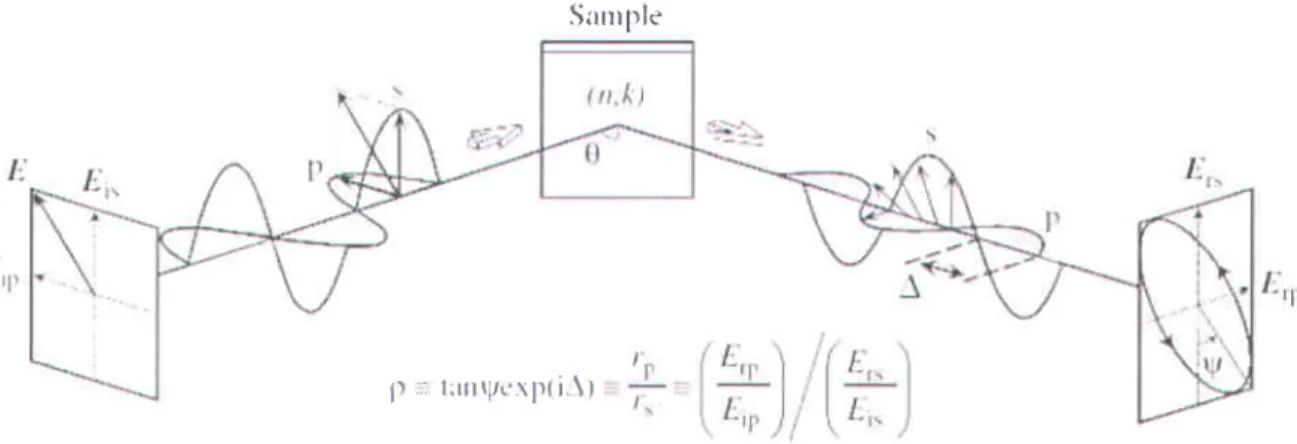
Ellipsometry is generally a non-invasive and non-destructive optical technique used for the measurement of the optical properties of a sample material. The principle of this technique is based on the change of the polarization state of light after reflection at oblique incidence on the surface under study. The measurement gives two independent parameters, y and A, which gives all relevant information about the polarization state of light at a given wavelength. 'Y' indicates the rate of amplitude of Fresnel coefficients ro and r. for the polarized light waves parallel with
the plane of incidence'p' and perpendicular to plane of incidence 's'. 'A' represents the phase difference between the above mentioned planes p and s, shown in Figure 2.6.|t does not depend on the absolute intensity as long as it is sufficient. This makes any measurement very precise and reproducible.
Here in our application, we used a new type of ellipsometry measurement named Variable Angle Spectroscopic Ellipsometry (VASE). It gives more comprehensive results since it studies materials over a wide spectral range. The main ellipsometric parameter, y and A are measured here by changing the wavelength of light guided by inbuilt VASE software. The incident angle of light is varied according to the optical constant of the sample in order to maximize the sensitivity of the measurement. However, there are two general limitations of spectroscopic ellipsometry measurement: the error increases if surface roughness goes above around 30o of the probe wavelength although it is completely dependent on the instrument type; and measurement must be done at oblique incidence, since otherwise (at normal incidence) it is very difficult, kind of impossible, to distinguish the'p' and's'planesl20l. The most crucial aspect of VASE ellipsometry is that it is an indirect charactenzation technique. Therefore, additional optical model with predefrned optical constants and sample layer thickness is requiredto analyze data. WVASE 32 software package of our instrument in this case stores a data base of refractive index for large number of materials.
Additionally, data analysis becomes difficult for the case of very thin frlm (< 10 nm) because of the difficulties of distinguishing between film and substrate. In addition, small absorption coefficient (a
depolarization), transparency of the films, films with high absorption, isotropic and anisotropic structure and many phases in the sample, fuither makes the characteization difficult. Therefore, another application called effective medium approximation (EMA) is added as optimization to obtain a minimum error.
Spectroscopic Ellipsometry allows measurements with a lateral resolution of - 100 microns to millimeters in lateral size, and it makes possible to measure a thickness of a layer of the sample of up to 50 pm. It also gives the extinction coefficient (k) as a function of wavelength (À)
S l r r r p l c
to measure the attenuation of light characterization followed by surface and
in the material. This technique enables additional interface, and layer inhomogeneity.
l ) r i , l l l i l r i / c \ l ) ( i . ' \ )
Figure 2.6 Schematic of the principle of Reflection Ellipsometry measurement [211
2.2.6 Solar Simulator (AM 1.5)
Radiation from the sun sustains life on the earth. The spectrum of radiation from the sun is somewhat similar to the blackbody radiation (5800k). The spectrum of solar radiation outside the earth's atmosphere is denominated as extraterrestrial. Once the spectrum enters into the earth's atmosphere it becomes terrestrial. Several factors affect the terrestrial spectrum such as location, atmospheric condition (cloud, aerosol content in the air, and ozone layer), distance between earth and sun, time of the day etc. Due to the large number of the involved variables on terrestrial solar spectrum, a standard spectrum has been developed to provide a basis for theoretical evaluation of the effects of solar radiation and as a basis for simulator design. The mostly used and accepted standard spectra are those published by The Committee lnternationale d'Eclaraige (CIE), the world authority on radiometric and photometric nomenclature and standards. Depending on the tilting of earth's surface, The American Society for Testing and Materials (ASTM) publish three spectra, AM0, 4M1.5 Direct and AM1.5 Global. Those spectra maintain a particular standard, for example, ASTM 8490, ASTM E891, ASTM 8892, ASTM 8927, and CIE pub.85 and904-3. Figure 2.7 gives a physical meaning and visualization of those spectra.
Here in our experiment we used SS50A.IAA solar simulator (class AAA) which consists of a high pressure Xenon Lamp (Xenon Short Arc) with 150 W power and a builtin touch panel color
![Figure 1.1 Schematics of different types of magnetic ordering [7]](https://thumb-eu.123doks.com/thumbv2/123doknet/5399495.125731/19.922.301.634.142.394/figure-schematics-different-types-magnetic-ordering.webp)


![Figure 2.a @) working principle of AFM technique (b) Force- distance curve plotted as a function of tip distance from the sample [16]](https://thumb-eu.123doks.com/thumbv2/123doknet/5399495.125731/39.922.220.713.135.353/figure-working-principle-technique-distance-plotted-function-distance.webp)
![Figure 2.7 (a) Definition of standard spectra [21] and (b) Schematics of typicalspectral22l](https://thumb-eu.123doks.com/thumbv2/123doknet/5399495.125731/44.922.187.754.322.536/figure-definition-standard-spectra-b-schematics-typicalspectral-l.webp)
