HAL Id: hal-01086621
https://hal.archives-ouvertes.fr/hal-01086621
Submitted on 24 Nov 2014HAL is a multi-disciplinary open access archive for the deposit and dissemination of sci-entific research documents, whether they are pub-lished or not. The documents may come from teaching and research institutions in France or abroad, or from public or private research centers.
L’archive ouverte pluridisciplinaire HAL, est destinée au dépôt et à la diffusion de documents scientifiques de niveau recherche, publiés ou non, émanant des établissements d’enseignement et de recherche français ou étrangers, des laboratoires publics ou privés.
Effect of doping on the modification of polycrystalline
silicon by spontaneous reduction of diazonium salts
A. Girard, Nathalie Coulon, Christophe Cardinaud, Tayeb
Mohammed-Brahim, Florence Geneste
To cite this version:
A. Girard, Nathalie Coulon, Christophe Cardinaud, Tayeb Mohammed-Brahim, Florence Geneste. Effect of doping on the modification of polycrystalline silicon by spontaneous reduction of diazonium salts. Applied Surface Science, Elsevier, 2014, 314, pp.358-366. �10.1016/j.apsusc.2014.07.012�. �hal-01086621�
Effect of doping on the modification of polycrystalline silicon by spontaneous reduction of diazonium salts
A. Girard*1, N. Coulon1, C. Cardinaud2, T. Mohammed-Brahim1, F. Geneste*3
1 UMR-CNRS 6164, Institut d’Electronique et de Télécommunications de Rennes, Université de Rennes 1, Campus de Beaulieu, 35042 Rennes cedex France
2 UMR-CNRS 6502, Institut des Matériaux Jean Rouxel, Université de Nantes, 2 rue de la Houssinière, BP32229, F-44322 Nantes cedex 3, France
3 UMR-CNRS 6226, Institut des Sciences Chimiques de Rennes, Equipe MaCSE, Université de Rennes 1, Campus de Beaulieu, 35042 Rennes cedex France
Abstract
The chemical modification of doped polycrystalline silicon materials (N+, N++ and P++) and silicon (100) and (111) used as references is investigated by spontaneous reduction of diazonium salts. The effectiveness of the grafting process on all polySi surfaces is shown by AFM and XPS analyses. The effect of substrate doping on the efficiency of the electrografting process is compared by using the thicknesses of the deposited organic films. For a better accuracy, two methods are used to estimate the thicknesses: XPS and the coupling of a O2 plasma etching with AFM measurement. Structural characteristics of the poly-Si films were investigated by Scanning Electron Microscopy and X-ray diffraction to find a correlation between the structure of the material and its reactivity. Different parameters that could have an impact on the efficiency of the grafting procedure are discussed. The observed differences between differently doped silicon surfaces is rather limited, this is in agreement with the radical character of the reacting species.
Keywords: Polycrystalline silicon, diazonium salt, spontaneous grafting, doping, crystallinity, functionalization
1. Introduction
Silicon is the most widely used material in semiconductor devices because of the low cost of its raw material, the relatively simple processing, and a useful temperature range. Polycrystalline silicon, also called PolySi, is composed of multiple small silicon crystals. It is a material of choice in microelectronics for the fabrication of devices needing deposition of doped silicon films. For
example, it is widely used in the fabrication of field effect transistors [1-5], solar panels [6] and diodes [7, 8]. Advantageously, the polySi deposition step is manufactured by Low Pressure Chemical Vapor Deposition (LPCVD), leading to deposited layers with good homogeneity, high stability and well-controlled doping concentrations. The process can also be performed at relatively low temperature allowing the deposition on many substrates like even glass.
The formation of organic thin films on silicon constitutes a major issue since it has been used in many electronic devices such as transistors, memories and diodes [9]. Among all the methods that have been developed to modify silicon surfaces [10-13], those involving radical reactions have the advantage to form a chemical bond directly on Si. Among them, the cathodic reduction of arenediazonium salts that has been widely used to functionalize surfaces [11, 14, 15] is particularly effective to prepare phenyl layers on H-terminated planar Si surfaces [16]. This efficient and fast grafting process leads to a strong covalent bond, and monolayers or thin films can be obtained in well-controlled conditions [17, 18]. Interestingly, the modification procedure can also be performed spontaneously, simplifying the process and making it readily accessible [19]. A mechanism has been proposed for the attachment of the aryl radical on hydrogenated Si surfaces (Scheme 1) [16].
Scheme 1 Si -Ar . .+ + Ar. + Si Si H H Si Si Si H H ArN2+ -N2 - H+ . Si Si Si H Si Si Si H Ar
The first step involves an electron transfer from the surface at open-circuit potential to the diazonium salt generating, upon loss of N2, an aryl radical. Elimination of a proton leads to silicon radical that reacts with aryl radical to give C-Si bond. The presence of silicon radicals has been confirmed through screening of various reagents known to react rapidly with molecular silicon radicals [20].
The reactivity of polySi substrates to spontaneous grafting of diazonium salts has been reported in literature [19, 21]. The electroless deposition can be performed both in the dark and under illumination. A better reactivity has been observed for polySi (N2+) than for Si (N2+) or Si (P2+) whatever the time exposure to the solution. It has been attributed to the roughness of the substrate giving rise to higher density of surface states, increasing the probability to ensure the spontaneous electron transfer leading to the reduction of the diazonium salt.
In view of the importance of polySi in the electronic devices fabrication, we investigated the effect of the nature and level of doping in polycrystalline silicon on the spontaneous reduction of
diazonium salts. The effectiveness of the grafting process was evaluated by XPS and AFM. The different substrates were analyzed by X-ray diffraction and SEM in order to find a correlation between the structure of the material and the reactivity of the surface toward the modification procedure.
2. Experimental section
2.1Chemicals
Reagents
4-carboxymethyl-benzenediazonium salts were prepared according to literature and stored under argon in a freezer [22]. All solvents were HPLC grade. Ultrapure water (18.2 Mω, Millipore Simplicity) was used for the grafting procedure.
Preparation of the modified surfaces
All manipulations were carried out under argon on a Schlenk line with standard airless techniques. A 2% hydrofluoric acid solution was cannulated into a reactor cell containing the surfaces under argon to remove the native Si oxide. After 2 min of immersion, the HF solution was eliminated. A solution containing 5 mg of 4-carboxymethyl-benzenediazonium salts in 50 mL of anhydrous deoxygenated acetonitrile was cannulated into the reactor cell. After 1h, the surfaces were washed in six successive baths of acetonitrile of 10 min each. It is worth noting that the grafted layer was still observed in XPS when the samples were sonicated 3 times in acetonitrile for 5 min. Before analyses, the samples were stored under argon in a fridge.
Substrates
In this work, three types of materials composed of silicon were studied.
As a reference, we add a silicon monocristal wafer, oriented 100, which is a microelectronic grade material (high purity) with well-known properties. This phosphorous-doped (1-10 ohm/cm) n-type Si has a thickness of 280 μm. It was purchased from BT Electronics.
The materials composed with silicon are deposited in the IETR laboratory on glass substrates. First, on this Corning Eagle glass substrates, a 250 nm buffer oxide layer was deposited by atmospheric pressure chemical vapor deposition (APCVD) technique at the temperature of 420°C with SiH4-N2-O2 gas mixture. This oxide layer acts as a diffusion barrier in order to avoid the possible contamination of the layers by impurities in the substrate.
Low Pressure Chemical Vapor Deposition (LPCVD)
The silicon layers (300 nm) were amorphously deposited at 550°C with a pressure of 90 Pa using a hot wall Low Pressure Chemical Vapor Deposition (LPCVD) reactor. Phosphorous (10 ppm or 1000 ppm PH3 diluted in hydrogen) and boron (1000 ppm B2H6 diluted in hydrogen)in situ doped silicon films are deposited with the same conditions using a mixture of silane as precursor gas and phosphine or diborane as a doping gas, respectively. Doping concentrations, measured by secondary ion mass spectroscopy (SIMS), are fixed at 3 × 10¹⁸ and 2 × 10²⁰ atom/cm3. After depositing each layer, a solid phase crystallization (SPC) process for 12h at 600°C under vacuum was carried out to obtain polysilicon.
All the conditions are summarized in Table 1.
Table 1 : LPCVD parameters
Layer types Diluted
PH3
Diluted B2H6
Pure SiH4 T°C Postbake°C
Weakly N-type polycristalline Si 17 - 50 550 600
Heavily N-type polycristalline Si 40 - 50 550 600
Heavily P-type polycristalline Si - 40 50 550 600
2.2 Instrumentation
AFM
The Atomic Force Microscopy (AFM) images were obtained in air, operating in tapping mode, using a Veeco AFM diCaliber High Value Scanning Probe Microscope with a standard antimony doped silicon tip which is a cantilever with a resonant frequency of 300 kHz. All the images were recorded with a 512 points per line resolution at a scan rate of 1Hz. Tapping mode was used to determine all the changes at the surface of our substrates caused by the grafting modification.
SEM
The SEM micrographs were obtained with a Jeol 6301F (9 kV) microscope. A scanning electron microscopy may be used not only to observe a surface image but also to provide a fine electron beam for charging an isolator surface simultaneously [23, 24].
X-Ray Diffraction (XRD)
X-Ray (Cu Kα) diffraction (Bruker D8 Advance) was used in the –2 configuration to evaluate : (i) the evolution of crystallization as a function of the doping
(ii) the existence of preferred grain orientations in the films XPS
X-Ray photoelectron spectroscopy (XPS) has been carried out with a Kratos Axis Ultra HSA spectrometer using a monochromatic Al Kα excitation (1486.6 eV), with magnetic confinement
charge neutralization, which is very effective in minimizing both uniform charging and differential charging on this large-band-gap semiconductor. The hybrid lens magnification mode was used with the slot aperture resulting in an analyzed area of 700 per 300 μm2. Charge stabilization was achieved by using the Kratos Axis device. The pass energy was set at 20 eV for the detailed scans. In these conditions, the energy resolution gives a full width at half maximum (FWHM) of the Ag 3d5/2 peak of about 0.55 eV. Wide scans were recorded with a step size of 0.5 eV and a pass energy of 80 eV, for narrow scans the corresponding parameters were 0.1 and 20 eV, respectively.
The sampling depth of approximately 15 nm in normal XPS analysis provides information on the nature of the chemical bonds of samples through the determination of core-level binding energies. To assess compositional variation with depth, angle-resolved XPS data were collected at nominal photoelectron take-off angles of 30° and 60°, where take-off angle is defined as the angle between the surface and the axis of the analyzer lens system. Using published electron mean free paths equations from Seah and Dench [25], the sampling depth (three times the mean free path) should decrease from ~ 11 to ~ 5 nm as the take-off angle decreases from 60° to 30°. The data were collected at room temperature, and the operating pressure in the analysis chamber was always below 10-9 Torr. Peak positions were referenced to the average reported data in the literature of aliphatic carbon (C-C/C-H 1s peak) at 285.0 eV [26-28].
Data treatment and peak fitting procedures were performed using Casa XPS software (version 2.3.16) and Kratos data base of relative sensitivity factors. Deconvolution of spectra into Gaussian-Lorentzian peaks (G/L=30), was also done using Casa XPS software, with peak area and width as free fitting parameters. A Shirley function was used to model the background. Peak assignments were made based on comparing the binding energies with reports in the literature for similar molecular species (Table 2).
Si (Si2p) Si-Si Si-C SiOx SiO2 99 – 99.6 101 102.7 103.5 - 103.7 [39] [40] [41] O (O1s) C=O Si-O-Si O-H SiO2 C-O-C 531.0 – 532.2 531.4 – 531.7 530.8 - 532.0 532.3 533.5 [40] [32] [33] [37] 3. Results
3.1 Characterization of the PolySi surfaces
3.1.1 Morphology and structure by Scanning Electron Micrograph
Heavily N-type polycristalline Si Heavily P-type polycristalline Si Weakly N-type polycristalline Si
Figure 1: Scanning electron micrographs of the surface of 300 nm-thick polysilicon films
Structural characteristics of the poly-Si films were investigated by Scanning Electron Microscopy (SEM). To investigate the morphology of the grains, the surfaces were treated by Secco etching, which is known to reveal grain boundaries and some defect clusters [42]. It is clear from these micrographs that the surface morphology was modified with doping. Comparison of Fig. 1 a) and b) shows the influence of the doping level on the grain size. Thus, heavily N-type poly-Si clearly presents smaller grains and more grain boundaries than the weakly N-type poly-Si. The nature of the doping also influences the structure of the surface. As highlighted in Fig. 1 a) and c), N-type poly-Si surfaces contain less grain boundaries than P-type poly-Si for similar doping concentrations. The presence of defects also seems to show that the P-type poly-Si is less well crystallized after the Secco treatment.
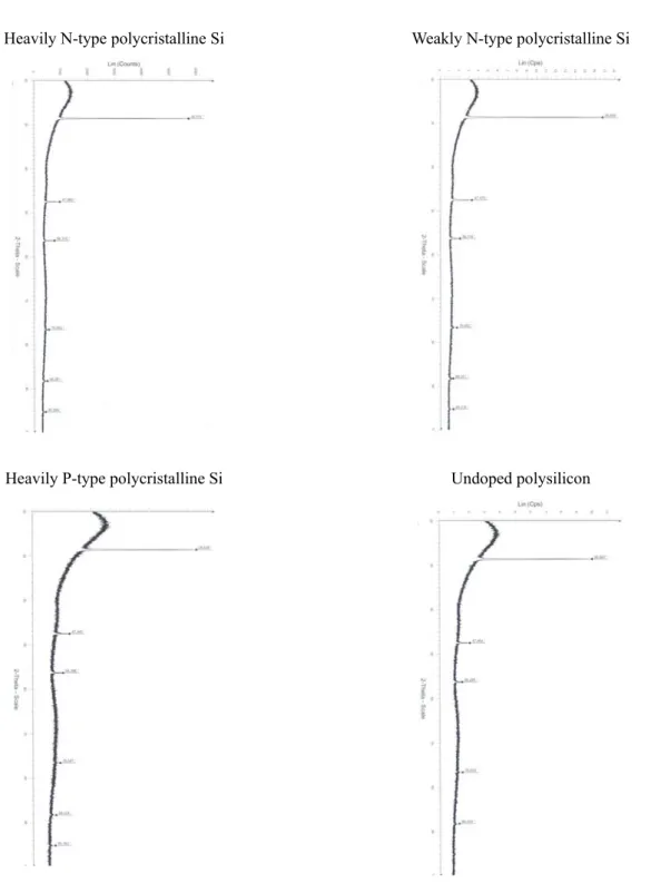
3.1.2. X-Ray diffraction
The crystallinity and preferred orientation (texture) of the deposited polysilicon films were studied by X-ray diffraction (XRD). Fig. 2 shows the X-ray diffraction profiles for undoped, N and P-doped films. The features for these LPCVD films are similar.
Heavily N-type polycristalline Si Weakly N-type polycristalline Si
Heavily P-type polycristalline Si Undoped polysilicon
The existence of preferred grain orientations were analyzed using the intensities of the (111), (220), (311), (331), (422) and (511) peaks (Table 3). These intensities were corrected to take into account the effect of the film thickness. The I(220)/I(111) and I(311) /I(111) intensity ratios were calculated and normalized to their values in a randomly oriented powder. A normalized ratio of one would indicate that the grains are randomly oriented. Values lower than one indicate a (111) preferred orientation.
Table 3 : Intensities of the Si peaks
(111) (220) (311) (400) (331) (422) (511) Weakly N-type polycristalline Si I 16.6 3.1 1.8 - 1.5 1.1 1.1 I/I(111) 1 0.18 0.11 - 0.09 0.06 0.06 Heavily N-type polycristalline Si I 19.2 2.9 2 - 1.6 1.5 0.9 I/I(111) 1 0,15 0,1 0.08 0.07 0.05 Heavily P-type polycristalline Si I 9.4 2.4 1.8 - 1.4 1.2 1.1 I/I(111) 1 0.25 0.19 - 0.15 0.13 0.12 Polysilicon I 11.9 2.1 1.6 - 1.6 1.3 -I/I(111) 1 0.18 0.13 0.13 0.11
For a randomly oriented polysilicon film, the X-ray integrated intensity of the (111) reflection is the strongest. For 300 nm-thick P type film, the other intensities for (220), (311), (400), and (331) reflections are lower by a factor of 0.25, 0.19, 0.18, and 0.06, respectively (Table 3).
3.2 Modification of the PolySi surfaces
PolySi surfaces were first treated with a 2% HF solution to achieve hydride termination. They were then immersed in a solution of 4-carboxymethyl-benzenediazonium salts in acetonitrile. Spontaneous reduction of the diazonium salt occurred, leading to surfaces functionalized by carboxylic acids (Scheme 2).
3.3 Characterization of the modified PolySi surfaces
3.3.1 XPS measurements
XPS measurements performed on the materials after immersion in the diazonium salt solutions reveal clearly that grafting occurs: all the spectra show photoelectron peaks characteristic of the diazonium salt used. Fig. 3 shows an example of wide-scan XPS for the unmodified and modified surface. 800 600 400 200 0 0 5000 10000 15000 20000 25000 30000 35000 40000 45000 50000
phenyl groups grafted on polycristalline Si
polycristalline Si Si 2s Si 2p C1s O1s In te n s ity ( c p s )
Binding energy (eV)
Figure 3: Survey scans of weakly N-type polycrystalline Si (black line) and substituted phenyl groups grafted on
polycrystalline Si (red line) with main peak assignment
Even if a C1s peak was observed in the spectra of polySi, probably due to pollution by oil vapor pumping LPCVD system or atmospheric contamination, grafting obviously leads to an increase of the C1s peak centered at 285.0 eV. The presence of an O1s peak at 532.4 eV in the polySi spectra is due to the reoxidation of the substrate before XPS analysis. We also noticed that photoelectron peaks characteristic of the semiconductor substrates (Si2s, Si2p) are attenuated but still visible after the organic layer has been grafted. This result indicates either the formation of a homogeneous layer onto the substrate the thickness of which is thinner than the depth analyzed by the XPS technique, or the heterogeneous distribution of the organic matter onto the surface.
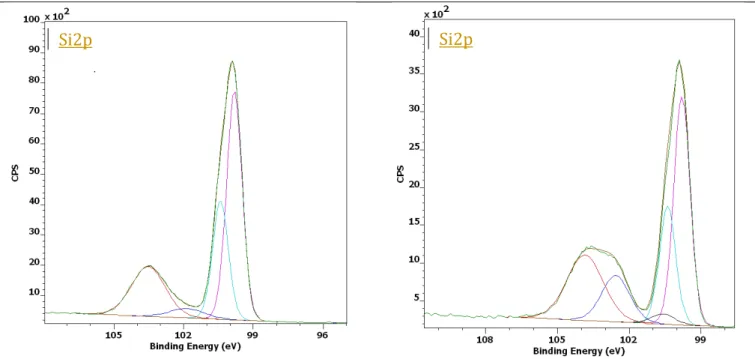
The presence of terminal grafted carboxylic functions was evidenced with XPS by analyzing C1s and Si2p core level. The high-resolution C1s spectra of the polycrystalline silicon and the modified sample are shown in Fig. 4. All data shown were obtained on N-type polycrystalline silicon; however, other dopings were measured and showed similar results. C1s spectra of the
polycrystalline silicon (Fig. 4a) can be decomposed into three features: one located at 284.8 eV assigned to C-C bonds, one at 286.7 eV assigned to C-O bonds and the last at 288.7 eV assigned to C=O bonds. With respect to the functionalized surface, the C1s peak at 285.2 characterized by C-C bonds increases significantly as a phenyl layer was grafted on the surface (Fig. 4b). The intensity of the peak around 287 eV, which is obviously attributed to the C-O bonds increased after grafting. Besides, we still observe the presence of the C=O peak (288.1 eV) and another one at 289.6 eV. This can be attributed to the functional group –COOH [10, 16]. Interestingly, a new carbon peak appears at 283.3 eV in the spectrum of the modified sample that corresponds to a carbide silicon. This small C1s signal is, however, really important as it was interpreted for many times in the literature as an evidence of the covalent metal-carbon bond between the metal surface and phenyl group grafted through the diazonium route [11, 28]. The peak found at around 283 eV was reported for the first time to be a direct proof for the existence of a covalent bond between an aryl group and the iron substrate [32]. The presence of Si-C bonds is also highlighted on the Si2p spectra with a component at 100.6 eV in the deconvolution (Fig. 4).
heavily N-type polycristalline Si heavily N-type polycristalline Si with grafted layer
Figure 4: Deconvolution of C1s and Si2p core level spectra obtained with AlK excitation
Angle-resolved XPS was performed to probe the interfacial species formed between the diazonium salt and the polysilicon surface. The analyzed depth (d) decreases following the relation [41]:
d = 3 λ cos a
where λ is the photoelectron mean free path for the analysed material, a is the photoelectron emission angle with respect to the detector axis; it is equal to the angle of sample rotation. Angular XPS analysis allows extinction of the signal from the deeper layers and hence, enhancement of the surface sensitivity. By this way, for thin-film deposits, depth resolution of different XPS detected bonds can be attained in order to permit a study of interfacial regions. The takeoff angles (TOAs) were 0, 30 and 60° relative to the surface normal.
Table 4 gives informations on elemental composition versus the TOAs.
Table 4: Analysis results of the grafted layer on heavily P type Poly Si by angular XPS (at%) depending of TOAs
TOAs (°) O (%) C (%) Si (%)
0 21 34.3 44.7
30 21.2 35 43.8
60 20.9 51.1 37
The silicon substrate is still visible even at 60°, an indication that the organic overlayer is thinner than the sampling depth of the technique. We observe an increase of the carbon content and a decrease of the silicon concentration (in the metallic and oxide forms). The oxygen concentration, however, is not affected by the angle, because this element belongs to both the inorganic substrate
as oxide forms and the organic overlayer in the form of COOH groups and superficial adventitious contamination.
The table 5 reports the concentrations (at%) of different types of bonds obtained after C1s decomposition region in function of the analysis angle.
Table 5: Peak fitting results for C1s region in function of the analysis angle
TOAs (°) C-Si (%) C-C/C-H (%) CH2-COOH (%) C-O (%) C=O (%)
C-Si/COOH ratio
0 1.4 82.5 8.2 5.5 2.4 0.17
30 1.2 86.0 7.4 3.8 1.6 0.16
60 1 87.7 7.3 2.9 1.1 0.14
From the results presented, it would appear that the carboxylic acid group is not exactly at the outermost surface of the organic layer because the relative intensity of the peak at 285.2 eV slightly decreases from 0 to 60°. Nevertheless, the carbide/COOH ratio (calculated from the results presented in Table 5) decreases versus the analysis angle, indicating that the COOH groups exist in all the thickness of the layer. This is in agreement with the formation of multilayers due to the growth of polyphenylene chains as it is well-known for grafting involving aryl radicals [43].
In addition to identifying elements present, XPS allows one to perform quantitative analysis.
Considering that a homogeneous layer is formed, the attenuation of the Si2p photoelectron signal
through the top layer yields insights into the molecular films thickness (z). This thickness (Table 6) could be estimated by the standard overlayer model [41]:
s
s I
I exp (-z/ λs cos a) = Isexp (-z/ λs sin θ)
Where Is is the intensity of the attenuated Si2p signal,
s
I is the Si
2p signal coming from the Si
sample without any overlayer, λs (nm) is the photoelectron mean free path of the substrate-specific
photoelectrons in the analysed material, a is the photoelectron emission angle with respect to the detector axis and θ is the analysis takeoff angle relative to the surface.
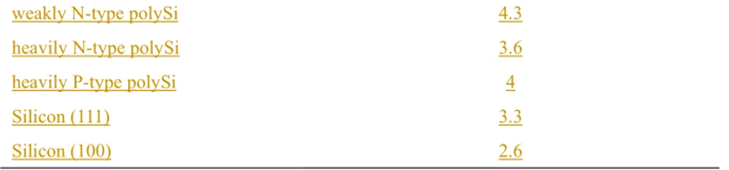
The electron attenuation length for Si was obtained from Henry de Villeneuve et al. [16], where the
λs value was equal to 4 ± 0.5 nm.
Table 6: Thickness (nm) of the grafted layer deduced from the attenuation of the signal
weakly N-type polySi 4.3
heavily N-type polySi 3.6
heavily P-type polySi 4
Silicon (111) 3.3
Silicon (100) 2.6
In the case of a polycrystalline silicon layer, the thickness of the grafted layer is about 4 nm against 2.6 nm and 3.3 nm for monocrystalline silicon oriented (100) and (111) respectively. It seems that the texture favors grafting as well as an (111) orientation.
3.3.2 By AFM
These results were corroborated by Atomic Force Microscopy (AFM). Contact mode AFM images of all surfaces have been performed before and after modification (8 m 8 m), as exemplified in Fig. 5 with weakly N-type polySi.
Figure 5: A top view representation of N-type polySi before (a) and after ( b) grafting.
Since surface roughness is a current factor to check the presence of a molecular layer on the surface, the RMS roughness of unmodified and modified polySi was also performed by measurements on 8 by 8 m images, in tapping mode AFM (Table 7).
The N-type polySi surface is flat and homogeneous showing topographical variations in the range 2 - 6 nm. Disperse nodules of approximately 0.1 - 0.2 m in diameter were observed. After grafting, the roughness changes appreciably giving rise to topographical variations of 5 to 7 nm, showing the effectiveness of the grafting process. The appearance of the modified surfaces is homogeneous with the presence of nodules with diameters between 0.05 and 0.36 m, in a larger amount than in the initial polySi surface. They can be attributed to the covering of the defects of polySi surfaces by a thin organic film after grafting. Whereas the roughness of Si (100) surfaces also increased after
grafting, the behavior of the heavily P-type polySi was different. Indeed, since its rugosity is high, the presence of the electrografting film probably smoothed the surface.
Table 7: RMS roughness of samples estimated by AFM
Layer types
weakly N-type polySi heavily N-type polySi heavily P-type polySi Silicon (111) Silicon (100)
The thicknesses of the grafting layers estimated by XPS were confirmed with a plasma etching followed by AFM analysis [44]. The method consists in mechanically masking the grafted surfaces and then exposing them to an oxygen plasma to etch the organic layer. The thickness of the resulting step (Fig. 6) corresponding to the transition between the grafting layer and the cleaned substrate was measured by AFM. Results are given in Table 8.
Table 8: Thickness (nm) of the grafted layer deduced from plasma etching coupled with AFM
Thickness of grafted diazonium layer (nm)a
weakly N-type polySi 4.5 ± 0.3
heavily N-type polySi 3.7 ± 0.4
heavily P-type polySi Silicon (111)
-Silicon (100) 1.9 ± 0.2
a
estimated from ten line measurements
The thickness measurement of the step was difficult to achieve on heavily P-type polySi and Si(111) due to the high roughness of the modified surfaces.
Figure 6: AFM images of a step created by O2 plasma etching on weakly N-type polySi and step measurement of the
grafted surface.
4. Discussion
XPS and AFM analyses were performed to investigate the effect of doping on the spontaneous grafting of diazonium salts on different silicon substrates. The increase of the C1s and O1s components in XPS associated with an attenuation of the Si peak evidenced the effectiveness of the grafting process on all the studied surfaces. The covalent immobilization of the aryl compound deduced from the stability of the organic layer to sonication in acetonitrile was confirmed by the presence of a peak corresponding to the C-Si bond. AFM images corroborated XPS analyses and highlighted the homogeneity of the organic film deposited on the surfaces. To evaluate the effect of doping on the grafting method, the surface thicknesses were estimated by XPS and by a method
combining a O2 plasma with AFM step measurements. Results obtained by the two different
process: weakly N-type polySi > heavily P-type polySi > heavily N-type polySi > Silicon (111) > Silicon (100). From these results, it is obvious that the method is less efficient on Si(100) and Si(111) than on polySi substrates, whatever the nature and amount of doping. This result is in accordance with those previously presented by Charlier et al. [21]. The authors have proposed that the higher roughness of the polySi surface, allowing a higher density of surface states, would explain its higher reactivity. However, our results do not exactly support this hypothesis since the more reactive surface is N-type polySi that is 3.4 times less rough than the heavily P-type polySi. A relationship between the surface electron work function and the crystal structure has already been evocated for electrografting of diazonium salts on polycrystalline gold substrate [45]. Since the work function is the minimum energy required to release electrons from the reactive surface, it is linked to the capacity to lose electrons of the different polySi substrates. Thus, the crystallinity of the polySi should influence the spontaneous reduction of the diazonium salt and so the effectiveness of the grafting process. X-ray diffraction allowed us to get insight into the crystallinity and preferred orientation of the deposited polysilicon films. None of the orientations of polySi seems to favor a grafting process in the order of reactivity revealed by thickness measurements: weakly N-type polySi > heavily P-N-type polySi > heavily N-N-type polySi. Since the integrated intensities of the (422) reflection in the different polySi substrates follow the opposite order, this orientation seems to be unfavorable to spontaneous grafting. By contrast, (220) and (511) orientations that predominate in the weakly N-type polySi would facilitate surface modification. However, it is difficult to conclude on the preferred orientation for spontaneous grafting on silicon from these results due to the combination of several orientations in polycrystalline Si. Pure material should be investigated to achieve a clear relationship between crystal structure of silicon and the effectiveness of spontaneous grafting of diazonium salts. Thus, the reactivity of Si(111) seems to be higher than Si(100), according to these experiments.
If the doping level plays a role in the resistivity of the material and so in the reactivity of the surface towards electrografting [46], it is not obvious for spontaneous reduction of diazonium salts. Indeed, the thickness of the grafted organic layer is higher for the weakly N-type polySi substrate than for the less resistant heavily N-type polySi surface. However, the nature and level of doping can influence other factors than resistivity. First, it affects the grain size of the polySi surface. Indeed, weakly N-type polySi has higher grain size than the heavily doped surfaces. Thus defects associated with grain boundaries could decrease the reactivity of the substrate, as if the grafting process preferentially occurred on the bulk surface. Second, the influence of doping on the Fermi level of polySi materials is well-known [47]. Thus, it has been shown that the Fermi level is significantly higher for weakly N-type polySi than for the heavily N-type polySi, which has also a higher Fermi level than the heavily P-type polySi. Furthermore, the spontaneous reduction of the diazonium salt
depends on the difference between the Fermi level of the doped semi-conductor and the LUMO of the diazonium salt. An increase of the Fermi level should lead to a more efficient reduction step and so to higher kinetics for the modification process. Indeed, a good correlation was found between the reactivity of the weakly and heavily N-type polySi substrates and their Fermi levels. However, for the heavily N and P-type polySi, the Fermi levels are closer and the crystal orientations play probably a more important role on spontaneous grafting.
5. Conclusion
Whereas covalent grafting by reduction of diazonium salts is now a common method to modify silicon substrates, this work focused on the modification of polycrystalline silicon by spontaneous reduction of diazonium salts and highlighted the effect of doping on the functionalization procedure. XPS and AFM analyses revealed that the covalent grafting process was very efficient on all studied polySi substrates, even more than on monosilicon Si(100) and Si(111) taken as references. Comparison of the thickness of the formed deposited organic layer showed that the effectiveness of the modification procedure followed the order: weakly N-type polySi > heavily P-type polySi > heavily N-P-type polySi. Whereas the resistivity does not influence the reactivity of the surface as for electrografting processes, other parameters such as the orientations of the crystal structure and the amount of grain boundaries can participate to the results. A good correlation between the measured surface thicknesses and the evolution of the Fermi levels with the doping level of the semi-conductor was also highlighted, underlining the role of the reducing power of the substrate for the effectiveness of the grafting procedure.
References
[1] G. Wenga, E. Jacques, A.-C. Salaün, R. Rogel, L. Pichon, F. Geneste, Biosens. Bioelectron. 40 (2013) 141.
[2] H. Mahfoz-Kotb, A. C. Salauen, F. Bendriaa, F. Le Bihan, T. Mohammed-Brahim, J. R. Morante, Sens. Actuators, B B118 (2006) 243.
[3] F. Bendriaa, F. Le Bihan, A. C. Salauen, T. Mohammed-Brahim, O. Bonnaud, J. Non-Cryst. Solids 352 (2006) 1246.
[5] R. Rogel, E. Jacques, L. Pichon, A.-C. Salaün, IEEE Transactions on Electron. Devices 61 (2014) 598.
[6] A. F. B. Braga, S. P. Moreira, P. R. Zampieri, J. M. G. Bacchin, P. R. Mei, Sol. Energ. Mat. Sol. Cells 92 (2008) 418.
[7] Z. Gaburro, Recent Res. Dev. Mater. Sci. Eng. 1 (2002) 493. [8] P. M. Fauchet, J. Lumin. 70 (1996) 294.
[9] H. E. Katz, J. Huang, Annu. Rev. Mater. Res. 39 (2009) 71.
[10] D. K. Aswal, S. P. Koiry, B. Jousselme, S. K. Gupta, S. Palacin, J. V. Yakhmi, Physica E 41 (2009) 325.
[11] J. Pinson, F. Podvorica, Chem. Soc. Rev. 34 (2005) 429.
[12] D. D. M. Wayner, R. A. Wolkow, J. Chem. Soc., Perkin Trans. 2 (2002) 23.
[13] S. Dauphas, S. Ababou-Girard, A. Girard, F. Le Bihan, T. Mohammed-Brahim, V. Vié, A. Corlu, C. Guguen-Guillouzo, O. Lavastre, F. Geneste, Thin Solid Films 517 (2009) 6016. [14] S. Dauphas, A. Corlu, C. Guguen-Guillouzo, S. Ababou-Girard, O. Lavastre, F. Geneste,
New J. Chem. 32 (2008) 1228.
[15] R. Marion, G. Muthusamy, F. Geneste, J. Catal. 286 (2012) 266.
[16] C. Henry de Villeneuve, J. Pinson, M. C. Bernard, P. Allongue, J. Phys. Chem. B 101 (1997) 2415.
[17] P. Allongue, C. Henry de Villeneuve, J. Pinson, F. Ozanam, J. N. Chazalviel, X. Wallart, Electrochim. Acta 43 (1998) 2791.
[18] P. Allongue, C. Henry de Villeneuve, J. Pinson, Electrochim. Acta 45 (2000) 3241.
[19] M. P. Stewart, F. Maya, D. V. Kosynkin, S. M. Dirk, J. J. Stapleton, C. L. McGuiness, D. L. Allara, J. M. Tour, J. Am. Chem. Soc. 126 (2004) 370.
[20] D. Wang, J. M. Buriak, Langmuir 22 (2006) 6214.
[21] J. Charlier, E. Clolus, C. Bureau, S. Palacin, J. Electroanal. Chem. 625 (2009) 97. [22] C. Bourdillon, J. Electroanal. Chem., 336 (1992) 113.
[23] H. Zhang, R. Feng, K. Ura, Sci. Prog. 87 (2004) 249.
[24] K. Kim, Z. Akase, T. Suzuki, D. Shindo, Mater. Trans. 51 (2012) 1080–1083. [25] M. P. Seah, W. A. Dench, Surf. Interf. Anal. 1 (1979).
[26] G. Beamson, D. Briggs, High resolution XPS of organic polymers-the science ESCA science database, John Wiley & Sons, Ltd, Chichester, 1992.
[27] J. E. Fulghum, J. Electron. Spectrosc. Relat. Phenom. 100 (1999) 331. [28] D. Bélanger, J. Pinson, Chem. Soc. Rev. 40 (2011) 3995.
[29] G. Collins, P. Fleming, C. O'Dwyer, M. A. Morris, J. D. Holmes, Chem. Mater. 23 (1211) 1883.
[30] T. Kuila, P. Khanra, S. Bose, N. H. Kim, B.-C. Ku, B. Moon, J. H. Lee, Nanotechnology 22 (2011) 305710/1.
[31] B. Chen, A. K. Flatt, H. Jian, J. L. Hudson, J. M. Tour, Chem. Mater. 17 (2005) 4832. [32] A. Adenier, M.-C. Bernard, M. M. Chehimi, E. Cabet-Deliry, B. Desbat, O. Fagebaume, J.
Pinson, F. Podvorica, J. Am. Chem. Soc. 123 (2001) 4541.
[33] K. Roodenko, M. Gensch, J. Rappich, K. Hinrichs, N. Esser, R. Hunger, J. Phys. Chem. B 111 (2007) 7541.
[34] P. Verma, P. Maire, P. Novak, Electrochim. Acta 56 (2011) 3555.
[35] K. Boukerma, M. M. Chehimi, J. Pinson, C. Blomfield, Langmuir 19 (2003) 6333.
[36] N. Graf, E. Yegen, T. Gross, A. Lippitz, W. Weigel, S. Krakert, A. Terfort, W. E. S. Unger, Surf. Sci. 603 (2009) 2849.
[37] T. Matrab, M. Save, B. Charleux, J. Pinson, E. Cabet-Deliry, A. Adenier, M. M. Chehimi, M. Delamar, Surf. Sci. 601 (2007) 2357.
[38] X. Wallart, C. H. de Villeneuve, P. Allongue, J. Am. Chem. Soc. 127 (2005) 7871. [39] Y. Narita, F. Hirose, M. Nagato, Y. Kinoshita, Thin Solid Films 517 (2008) 209. [40] C. Chen, J. Liu, B. Yu, D. Zhu, Electron. Mater. Lett. 3 (2007) 63.
[41] D. Briggs, M. P. Seah, Practical Surface Analysis by Auger and X-Ray Photoelectron Spectroscopy, Wiley, New-York, 1983.
[42] F. Secco d'Aragona, J. Electrochem. Soc. 119 (1972) 948.
[43] C. Combellas, F. Kanoufi, J. Pinson, F. I. Podvorica, Langmuir 21 (2005) 280.
[44] A. Girard, F. Geneste, N. Coulon, C. Cardinaud, T. Mohammed-Brahim, Appl. Surf. Sci. 282 (2013) 146.
[45] A. Benedetto, M. Balog, P. Viel, F. Le Derf, M. Sallé, S. Palacin, Electrochim. Acta 53 (2008) 7117.
[46] F. Le Floch, M. Matheron, F. Vinet, J. Electroanal. Chem. 660 (2011) 127. [47] A. Zur, T. C. McGill, D. L. Smith, J. Vac. Sci. Technol. B 1 (1983) 608.