Université de Québec
Institut National de la Recherche Scientifique Énergie Matériaux Télécommunications
Synthesis and Functional Properties of BiFeO
3and
Bi
2FeCrO
6based Nanostructures and Thin Films
Shun Li
Thèse présentée pour l’obtention du grade de Philosophiæ Doctor (Ph.D.) en Sciences de l’énergie et des matériaux
Jury d’évalauation
Président du jury Andreas Ruediger et examinateur interne INRS ÉMT
Examinateur externe Nazir Kherani
Université de Toronto Examinateur externe Pablo Bianucci Université Concordia Directeur de recherche Federico Rosei INRS ÉMT
Contents
Abstract ... 1 Acknowledgements ... 5 List of Figures ... 7 List of Tables ... 15 Chapter 1. Introduction ... 16 1.1 Basics ... 16 1.1.1 Perovskite Oxides ... 16 1.1.2 Ferroelectricity ... 19 1.1.3 Magnetism ... 21 1.1.4 Multiferroic Materials ... 22 1.2 BiFeO3 ... 261.2.1 Crystal Structure and Physical Properties of BiFeO3 ... 26
1.2.2 BiFeO3 Nanomaterials ... 30
1.2.2.1 Synthesis of BiFeO3 Thin Films and Nanostructures ... 31
1.2.2.2 Size Effects in BiFeO3 Nanostructures ... 32
1.3 Bi2FeCrO6 ... 34
1.3.1 Synthesis and Characterizations of Bi2FeCrO6 ... 36
1.3.2 Multiferroic Properties of Bi2FeCrO6 ... 39
1.4 Multiferroic Materials for Solar Energy Conversion ... 42
1.4.1 Multiferroic Materials for Photovoltaic Applications ... 44
1.4.1.2 Bulk Photovoltaic Effect in Ferroelectrics ... 46
1.4.1.3 Advances in Multiferroic Materials for Photovoltaic Applications ... 49
1.4.2 Multiferroic Materials for Photocatalytic Water Splitting Applications ... 52
1.4.2.1 Photocatalytic Water Splitting by Powder Semiconductors ... 53
1.4.2.2 Photoelectrochemical Water Splitting by Semiconductor Electrodes ... 55
1.4.2.3 BiFeO3 for Photocatalysts and Photoelectrodes ... 58
Chapter 2. Research Objectives and Thesis Organization ... 63
2.1 Research Objectives ... 63
2.2 Thesis Organization ... 65
Chapter 3. Experimental Methods ... 68
3.1 Materials ... 68
3.2 Synthesis Techniques ... 69
3.2.1 Conventional Hydrothermal Synthesis ... 69
3.2.2 Microwave-assistant Hydrothermal Synthesis ... 70
3.2.3 Pulsed Laser Deposition ... 71
3.3 Characterizations ... 73
SECTION (І) Synthesis and Functional Properties of BiFeO3 based Nanostructures Chapter 4. Ferroelectric Properties of Single Crystalline BiFeO3 Nanowires (NWs) ... 79
4.1 Experimental Section ... 80
4.2 Structural and Morphological Characterizations ... 81
4.3 Ferroelectric Properties ... 82
4.4 Discussion ... 85
4.5 Summary ... 88
Chapter 5. Highly Active Nanocomposite Photocatalyst Consisting of BiFeO3 Nanowires and Laser Ablated Au Nanoparticles (PLAL-AuNPs) ... 89
5.1 Experimental Section ... 91
5.1.1 Materials Synthesis ... 91
5.1.1.1 Synthesis of AuNPs by Laser Ablation in Liquid (PLAL-AuNPs) ... 91
5.1.1.3 Preparation of Hybrid AuNPs/BiFeO3 Nanowires Nanocomposites ... 92
5.1.2 Photocatalytic Water Splitting Measurements ... 93
5.2 Characterizations ... 93
5.3 Photocatalytic Water Splitting Performance ... 97
5.4 Proposed Mechanism ... 101
5.5 Summary ... 104
Chapter 6. Microwave-assistant Hydrothermal Synthesis and Magnetic Properties of BiFeO3 Nanoplates ... 105
6.1 Synthesis of BiFeO3 Nanoplates ... 108
6.2 Characterizations of BiFeO3 Nanoplates ... 108
6.3 Effect of Synthesis Parameters on BiFeO3 Nanoplates ... 112
6.3.1 Effect of Radiation Power and Energy... 112
6.3.2 Effect of Alkali Concentration ... 114
6.3.3 Effect of Reaction Time ... 116
6.4 Proposed Formation Mechanism ... 117
6.5 Magnetic Properties of BiFeO3 Nanoplates ... 118
6.6 Summary ... 120
SECTION (ІІ) Bi2FeCrO6 Thin Films for Solar Energy Conversion Applications Chapter 7. Photovoltaic Effect in Epitaxial Bi2FeCrO6 Thin Films ... 121
7.1 Experimental Section ... 123
7.1.1 Deposition of Bi2FeCrO6 Thin Films ... 123
7.1.2 Device Fabrication and PV Measurements ... 123
7.2 Characterizations of Bi2FeCrO6 Thin Films... 124
7.3 Optical Properties of Bi2FeCrO6 Thin Films... 130
7.3.1 Effect of Cationic Ordering on Optical Properties ... 131
7.3.2 Effect of Ordered Domain Size on Optical Properties ... 133
7.4 Ferroelectric Properties of Bi2FeCrO6 Thin Films ... 135
7.5 PV Properties of Bi2FeCrO6 Thin Films ... 137
Chapter 8. Photoelectrochemical (PEC) Properties of Epitaxial Bi2FeCrO6 Thin Films ... 143
8.1 Experimental Section ... 145
8.1.1 Deposition of Bi2FeCrO6 Epitaxial Thin Films ... 145
8.1.2 PEC Measurements ... 146
8.2 Characterizations ... 147
8.3 PEC Performance ... 154
8.3 Summary ... 161
Chapter 9. Conclusions and Perspectives ... 163
9.1 Conclusions ... 163
9.2 Perspectives ... 166
Appendix A: List of Acronyms ... 198
Abstract
There is an increasing interest in developing and characterizing multiferroic materials, in which
both ferromagnetic and ferroelectric orders coexist, as they exhibit rich physical properties and
offer exciting opportunities for data storage, spintronics, sensors, electromagnets and
photovoltaic (PV) applications. Among all multiferroic materials studied so far, BiFeO3 (BFO)
has attracted considerable attention because it shows intrinsic ferroelectric (TC ~ 1103 K) and
G-type antiferromagnetic (TN ~ 643 K) orders simultaneously well above room temperature. In
addition, multiferroic BiFeO3, with band gap energy of 2.2-2.8 eV,has been recently identified
as a promising candidate for PV devices and photocatalysts in the visible range.Moreover, the
coupling between ferroic orders in BiFeO3 materials offers new modes for investigating and
controlling the PV effect, which may endow next generation solar and photoelectrochemical
(PEC) cells with multiple functionalities. On the other hand, considerable interest has been
attributed to multiferroic BiFeO3 nanostructures in the quest of miniaturizing devices and
discovering interesting fundamental physics at nanoscale. BiFeO3 nanomaterials with various
sizes and shapes such as nanoparticles, nanotubes, nanowires, and nano-/micro cubes have been
reported so far and exhibit quite different physical and chemical properties compared to the bulk
form of BiFeO3 crystals due to the nanosize effect. Therefore, the synthesis of multiferroic
for both fundamental research as well as designing new multifunctional materials combining
magnetic, ferroelectric and optoelectronic properties.
Meanwhile, recent emergence of a novel double perovskites multiferroic material Bi2FeCrO6
(BFCO), with functional properties well above room temperature, opens new opportunities for
practical applications of multiferroics. Bi2FeCrO6 has a similar crystal structure as BiFeO3 and
exhibits a particularly Fe/Cr cationic ordering along the [111] pseudocubic direction. Recent
works demonstrated that an ordered Bi2FeCrO6 phase can be obtained in both thin film and
nanostructured form using pulsed laser deposition (PLD) technique.The reported Bi2FeCrO6 thin
films possess a remnant polarization of about 55 C/cm2 along the [001] pseudocubic direction,
and are ferrimagnetic with a magnetic moment depending on Fe/Cr cationic ordering, about 1.8
B per formula unit, far exceeding the properties of parent BiFeO3. In addition, theoretical
studies showed that Fe and Cr mixed d orbital transition allow a small band gap around 2.3 eV.
Therefore, Bi2FeCrO6 is expected to be a promising candidate for efficient PV devices and PEC
cells using sun light.
The work performed in this thesis was therefore driven by two main objectives: (1) synthesis
and understanding the fundamental physical properties (i.e. ferroelectric and magnetic) of
various low-dimensional BiFeO3 nanostructures; (2) design and investigate BiFeO3 and
Bi2FeCrO6 basednanomaterials and thin film devices for high efficiency solar energy conversion
(solar to chemical/electrical energy) applications. The results obtained in this work are resumed
in two sections as follows:
In the first section, we have synthesized and investigated the ferroelectric, magnetic and
studied the ferroelectric properties of 1D single-crystalline BiFeO3 nanowires using
piezoresponse force microscopy (PFM). PFM measurements demonstrated that the
as-synthesized BiFeO3 nanowires, down to 40 nm in diameter, have components of spontaneous
polarization along both in plane and out of plane directions, thereby confirming the ferroelectric
nature of the wires. We explained our results by estimating the shape of the piezoelectric tensor
for the rhombohedral symmetry. We have also studied the photocatalytic solar water splitting
properties of the BiFeO3 nanowires and discovered that the nanowires exhibit better
visible-light-driven photocatalytic activity for generation of O2 from water than other BiFeO3 materials (e.g.
nanocubes) reported previously, which could be attributed to the unique morphology of the
nanowires. To further enhance the photocatalytic activity, we designed and synthesized a hybrid
Au/BiFeO3 nanocomposite photocatalyst consisting of single crystalline BiFeO3 nanowires and
laser ablated Au nanoparticles by a functionalization-step-free solution process. We found that
1.0 wt% Au nanoparticle decorated BiFeO3 nanowires exhibit significantly higher photocatalytic
activity (~30 times) of water oxidation for O2 than that of the parent wires during the first 4 h of
the reaction. Their superior catalytic activity can be attributed to the role of the Au as electron
trapping centers as well as the unique surface-chemistry features of the laser ablated Au
nanoparticles that can strengthen the interaction and promote charge transfer. Meanwhile, we
observed that the localized surface plasmonic resonance (LSPR) effect of Au nanoparticles could
also contribute to the enhancement of the photoactivity. In addition, we developed a novel
approach to synthesize (100) pseudocubic facets exposed 2D single crystalline BiFeO3
nanoplates, with thickness ranging from 20 to 120 nm and lateral size of sub-micrometers, via a
weak ferromagnetic properties at room temperature, which we attribute to the size-confinement
effect on magnetic ordering.
The second section is focused on solar energy conversion (i.e. PV and PEC) applications of
Bi2FeCrO6 thin film based cells. First, we presented the optical and PV properties of Bi2FeCrO6
epitaxial thin films grown on (100)-oriented SrTiO3 substrate buffered with SrRuO3 electrode
deposited via PLD. In this part of work, we have achieved a wide band gap tunability from 1.4 to
2.5 eV in the epitaxial Bi2FeCrO6 films with significant polarization by tuning the ordering of
transition-metal element Fe and Cr cations, which is remarkably large as compared with reported
values from other doped ferroelectrics, opening up the possibility of discovering new narrow
band gap multiferroic materials and designing high efficient oxide solar cells. With optimized
PLD deposition conditions, we got a record power conversion efficiency of 3.3% under AM1.5G
illumination (100 mW/cm2) in the Bi2FeCrO6 thin film based solar cells. Additionally, we
demonstrated the use Bi2FeCrO6 epitaxial thin film as a new photocathode material for the
visible-light-driven reduction of water to hydrogen. PEC measurements showed that the highest
photocurrent up to −1.0 mA/cm2 at a potential of −1.0 V versus reversible hydrogen electrode
(RHE) was obtained in p-type Bi2FeCrO6 thin film grown on CaRuO3/SrTiO3 substrate. For the
positively poled Bi2FeCrO6 thin film, the photocurrent density was further enhanced by a factor
of ~2, as a result of the modulation of the internal electric field gradient resulting from the
Acknowledgements
First I would like to thank my advisor, Prof. Federico Rosei, for continual guidance and
assistance throughout the duration of my Ph.D., and without whom this work would not have
been possible. Professionally, Dr. Rosei launches my scientific career, to which I am determined
to dedicate the rest of my life. And personally, he has always been a strong supporter when I
need help. Being able to study under his supervision is one of the most important achievements
in my life.
I would also wish to give special thanks to the contributions to this work made by Dr. Riad
Nechache. He made vital contributions to most of the work and gave me invaluable help and
comments on my research and thesis writing. I am also grateful to all the group members from
NFL for their help throughout the work. These people include: Wei Huang, Joyprokash
Chakrabartty, Daniel Obi, Driss Soubane, Catalin Harnagea, Liliya Nikolova, Jonathan
Laverdiere, Kadiatou Thérèse Dembélé, as well as other collaborators including Jianming Zhang,
Md Golam Kibria, Bandar AlOtaibi, Menouer Saidani and Ivan Alejandro Velasco Davalos.
I would like to acknowledge Prof. Andreas Ruediger and Prof. Dongling Ma at INRS-EMT,
and Prof. Zetian Mi from McGill University for their kind help and important comments on my
A massive thanks to all my friends who have made the last four years so enjoyable: Guozhu
Chen, Yue Huang, and Belete Atomsa, etc., without you I cannot have such wonderful memories
these years.
I thank to the departmental and technical staff at INRS-EMT. They are very helpful,
particularly Christophe Chabanier. I also would like to acknowledge Jean-Philippe Masse at
Ecole Polytechnique for TEM measurements.
I am indebted to my dearest parents, for their constant support and encouragement
throughout all of my studies. I wish to thank to my wife, Heping Fan, who loves me deeply and
supports me selflessly. I thank my family and my friends for their continuing love and heartily
support.
Finally, I wish to acknowledge the following organizations for their financial support to my
research: the Natural Sciences and Engineering Research Council of Canada and Canada
Foundation for Innovation. I also highly appreciate the support from the China Scholarship
Council (CSC) and Fonds québécois de la recherche sur la nature et les technologies (FQRNT)
List of Figures
Figure 1. Two typical views of ideal cubic ABO3 perovskite structure unit cell, where the green, the blue
and red spheres represent A, B cations and oxygen, respectively. The structure of an ABO3 perovskite with
the origin centered at (a) the B-site ion and (b) the A-site ion [2]. ... 17
Figure 2. The schematic diagram of double perovskites structure of the general formula A2BB′O6 [16]. . 19
Figure 3. Atomic structures of perovskite oxides ABO3 in the paraelectric phase and ferroelectric phase
with upward and downward polarization [19]. ... 20
Figure 4. Schematic diagrams showing the spins of (a) ferromagnet, (b) antiferromagnet, (c) ferrimagnet
and (d) canted antiferromagnetic, where the magnetic components in different directions are represented by dashed arrows. ... 22
Figure 5. Portrayal of multiferroics possessing magnetic and ferroelectric properties [29]. ... 23 Figure 6. Classification of insulating oxides. The largest circle represents all insulating oxides among
which one finds electrically polarizable materials (green ellipse) and magnetically polarizable materials (orange ellipse). Within each ellipse, the circle represents materials with a finite polarization
(ferroelectrics) and/or a finite magnetization (ferro- and ferrimagnets). Depending on the definition, multiferroics correspond to the intersection between the ellipses or the circles. The small circle in the middle denotes systems exhibiting a magnetoelectric coupling [37]. PZT represents PbZrxTi1-xO3. ... 24
Figure 7. Schematic drawing of the crystal structure of perovskite BiFeO3 (space group: R3c) [24]. Two
unit cells along the [111] direction are shown in the figure. ... 27
Figure 8. (a) Magnetic hysteresis loop for a BiFeO3 film of 70 nm thickness (blue data is in plane, red
data is out of plane of the film), and (b) electric hysteresis loop for a BiFeO3 film of 200 nm thickness,
measured at a frequency of 15 kHz. All data was measured at room temperature. Adapted from [24]. .... 28
Figure 9. Portion of hexagonal BiFeO3 lattice. The arrows indicate the Fe3+ moment direction [56]. ... 29
Figure 10. Schematic representation of the spin cycloid of BiFeO3. The canted antiferromagnetic spins
to zero due to the cycloidal rotation. The spins are contained within the plane defined by the polarization vector (red) and the cycloidal propagation vector (black) [58]. ... 30
Figure 11. M-H hysteresis loops of BiFeO3 nanoparticles with various sizes at room temperature [69]. . 33
Figure 12. Magnetic microdomains in double perovskites A2BB'O6 materials, where Fe3+ and Cr3+ are
located in the B and B' sites [93]. ... 34
Figure 13. (a, b) Sketch of the double-perovskite crystal structure and (c) corresponding pseudo-cubic
unit cell of Bi2FeCrO6. Adapted from [101]. ... 35
Figure 14. (a) Pressure-temperature phase diagram for thin films of the Bi-Fe-Cr-O system with a
nominal thickness of 90 nm. (b) Oxygen pressure-substrate temperature data points in the phase diagram for which pure phase Bi2FeCrO6 films are obtained together with the vapour pressure curve of metallic Bi
drawn in the same diagram [109]. ... 37
Figure 15. (a) RSM scan around (111) reflection recorded for (001) oriented Bi2FeCrO6 films. (b) θ/2θ
XRD scans of Bi2FeCrO6 thin films on SrTiO3 (111) at different growth temperatures. Different types of
Fe and Cr octahedral stacking in Bi2FeCrO6 along (c) the [001] and (d) the [111] cubic directions.
Adapted from [101]. ... 38
Figure 16. (a) Magnetization hysteresis of Bi2FeCrO6 film compared to that of BiFeO3 film at room
temperature. The direction of applied magnetic field H was in the plane of the films. (b) Current vs. applied voltage curve and the corresponding ferroelectric hysteresis loop and obtained at room temperature for a 200 nm thick Bi2FeCrO6 thin film. The solid line corresponds to the polarization
hysteresis loop after subtracting the leakage contribution. Adapted from [104, 109]. ... 39
Figure 17. (a) Magnetic hysteresis loops of various Bi2FeCrO6 thin films prepared with different
deposition conditions but all prepared with deposition conditions within the phase diagram region where single phase Bi2FeCrO6 is obtained, as indicated by the open circles labelled P1 to P6 in the phase
diagram (Fig. 14a). The inset shows an enlarged figure. (b) Relationship between the degree of ordering in Fe/Cr estimated from the I111/I222 ratio and the saturated magnetization measured at room temperature
(Applied magnetic field is in-plane). The inset shows RSM-extracted profile lines around the (111) superstructure reflection obtained for the different films [109]. ... 40
Figure 18. (a) SEM image showing a well-defined array of square Bi2FeCrO6 nanostructures. (b) SEM
image of a typical Si3N4 membrane nanostencil. (c) In plane (IP) and out of plane (OP) magnetic
hysteresis loops for the whole patterned area of Bi2FeCrO6 structures at room temperature. (d)
Piezoresponse hysteresis loop recorded from an individual Bi2FeCrO6 island in OP-PFM mode. Adapted
from [111]. ... 41
Figure 19. Comparison of various solar energy conversion technologies [113]. ... 43 Figure 20. Typical current-voltage (I-V) curve of a solar cell with and without illumination [122]. ... 44
Figure 21. NREL compilation of best research solar cell efficiencies [123]. ... 45 Figure 22. Simplified schematics of PV mechanism in (a) semiconductor p-n junction and (b)
ferroelectric thin film [131]... 47
Figure 23. The absorption coefficient α(E) of BiFeO3 nanoparticles (average grain size of ~16 nm) as
compared with that of an epitaxially grown rhombohedral thin film. Inset: direct band gap analysis. Blue dashed arrows denote the charge transfer excitation split by 0.5 eV [156]. ... 49
Figure 24. (a) PFM image showing well-aligned arrays of domain walls in an epitaxial BiFeO3 film. The
domains of opposite electrical polarization are 150 nm wide, and the walls between them (light contrast) are 2 nm in width. (b) Schematic band structure and PV current flow. Adapted from [151, 158]. ... 50
Figure 25. Dark and red light illumination J-V measurements curves revealing a PV effect in the
Bi2FeCrO6 epitaxial films. The top-left inset displays a schematic of the device. The bottom-right inset is
a zoom around zero indicating the maximum current density and open circuit voltage used for the
calculation of the efficiency [166]. ... 52
Figure 26. Fundamental principle of semiconductor-based photocatalytic water splitting for hydrogen
generation [170]. NHE represents reversible hydrogen electrode. ... 53
Figure 27. Main processes in photocatalytic water splitting [170]. ... 54 Figure 28. Band-edge positions of semiconductor photocatalysts relative to the energy levels of various
redox couples in water [169]. ... 55
Figure 29. Photoelectrochemical water splitting systems using (a) n-type semiconductor photoanode, and
(b) p-type semiconductor photocathode. Adapted from [182]. ... 56
Figure 30. Theoretical photocurrent densities for semiconductors under one-sun illumination. The blue
curve is the integrated photon flux at different cutoff energies, based on the AM1.5G solar spectrum [183]. ... 57
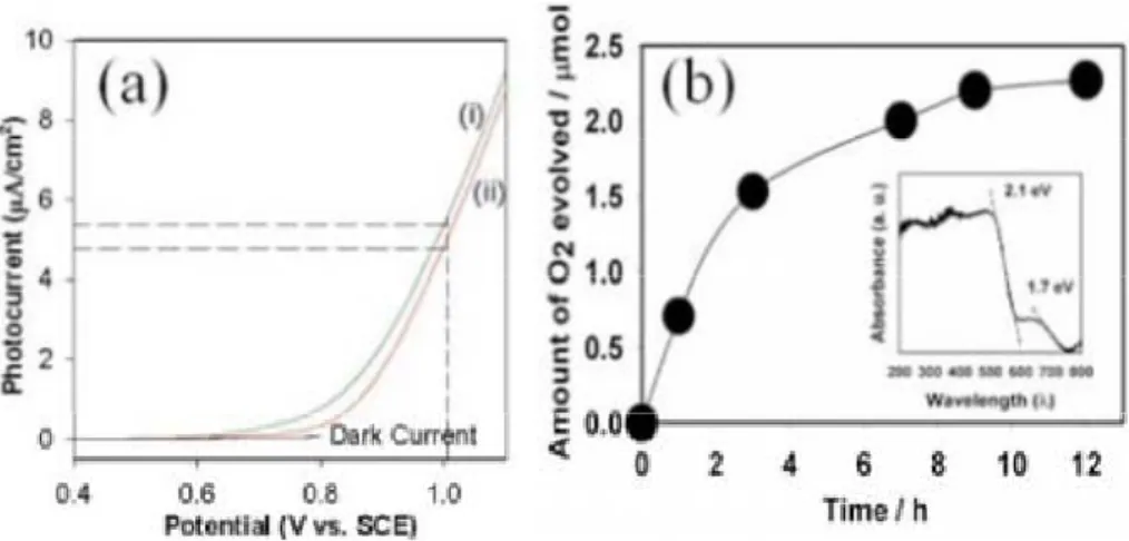
Figure 31. (a) Photocurrent density-potential curves of (i) BiFeO3 nanocubes and (ii) BiFeO3 bulk thin
film electrodes under visible illumination. (b) Photocatalytic oxygen evolution under visible light irradiation over BiFeO3 nanocubes. Inset shows photoabsorption spectrum of the BiFeO3 nanocubes.
Light source is a 500 W Hg lamp with a cutoff filter of 420 nm [81]. ... 59
Figure 32. (a) Current-potential dependence of the BiFeO3 film electrode under visible-light irradiation
(λ > 420 nm, light intensity: 60 mW/cm2). Solid line for the polycrystalline film and dashed line for the amorphous film. (b) IPCE (incident photon to charge carrier efficiency) of the polycrystalline BiFeO3
film electrode measured at different potentials: (1) 1.5 V, (2) 1.2 V, (3) 0.8 V, (4) 0.5 V, and (5) 0.2 V. Adapted from [196]. ... 60
Figure 33. Linear sweep voltametry curves of BiFeO3/SrRuO3/SrTiO3 (001) with different ferroelectric
polarizations. Black: negative polarization charges on the surface; red: positive polarization charges on the surface [197]. ... 61
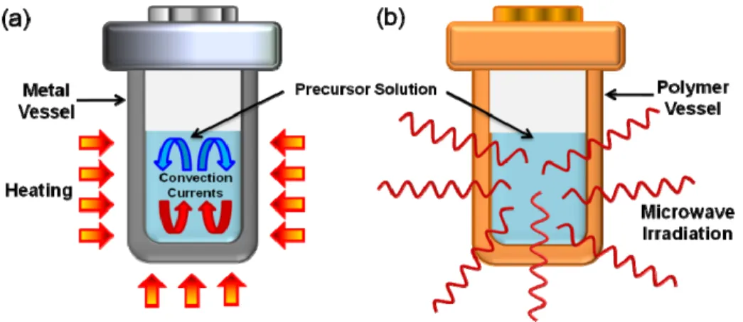
Figure 34. (a) A schematic cross section view of a Teflon-lined, stainless autoclave [203]. (b) A
photograph showing the components of a typical autoclave for hydrothermal synthesis. ... 69
Figure 35. Schematic illustration of the two modes of hydrothermal synthesis technique: (a) conventional
hydrothermal (C-H) and (b) microwave-assisted hydrothermal (M-H). ... 71
Figure 36. Schematic of a standard pulsed laser deposition system. The inset picture shows an actual
photograph of the plume [27]... 72
Figure 37. Experimental setup of PFM measurement [208]. ... 78 Figure 38. (a) XRD pattern of as-synthesized BiFeO3 nanowires powders. Inset shows the crystal
structure of BiFeO3. (b) A typical SEM image of the nanowires [198]. (c) Representative TEM image of
an individual nanowire. Inset: electron diffraction patterns taken from the nanowire. (d) HRTEM image taken from the edge of the nanowire in (c). ... 81
Figure 39. Three-dimensional AFM topographic image representation of an individual nanowire lying on
platinum coated silicon substrate surface. The inset shows the corresponding scanline taken along the solid white line crossing the nanowire [198]. ... 82
Figure 40. An example of PFM phase-voltage hysteresis and amplitude-voltage “butterfly” loops of an
individual BiFeO3 nanowire in (a) z- (out of plane) and (b) x- (in plane) direction, respectively [198]. .... 83
Figure 41. (a-c) PFM hysteresis loops (x and z-direction) taken from the nanowires shown in each figure,
respectively. (d) Schematic diagram showing the relative geometry position between [111]c direction in
the nanowires and the substrate [198]. ... 85
Figure 42. Calculated piezoelectric tensor for the longitudinal piezoresponse dzz (a) and lateral
piezoresponse dzxz (b). (c) Cross-section of (b) in the 110 plane, containing the spontaneous
polarization [198]. ... 86
Figure 43. Schematic diagram for synthesizing PLAL-AuNPs/BiFeO3 nanowires hybrid nanostructures
[199]. ... 91
Figure 44. Zeta-potential of BiFeO3 nanowires and PLAL-AuNPs aqueous solution at different pH values
[199]. The solid line is to guide the trend of the measured points. ... 93
Figure 45. (a) SEM and (b) TEM images of the BiFeO3 nanowires. (c) TEM and (d) HRTEM images of
the PLAL-AuNPs (1.0 wt%) decorated BiFeO3 nanowires, respectively. (e) SAED pattern taken from (c)
[199]. ... 94
Figure 46. XPS spectra of Au4f in pristine PLAL-AuNPs and PLAL-AuNPs (1.0 wt%)/BiFeO3
Figure 47. (a) Normalized UV-vis absorption spectra of BiFeO3 nanowires and PLAL-Au(1.0
wt%)/BiFeO3 nanowires nanocomposite dispersed in ethanol. (b) Calculation diagram of the band gap of
BiFeO3 nanowires [199]. ... 96
Figure 48. Oxygen evolved upon visible light (λ > 380 nm) illumination of FeCl3 suspension (4 mmol/L,
50 mL) containing the photocatalysts (50 mg) [199]. ... 97
Figure 49. TEM images of (a) PLAL-AuNPs and (b) Chem-AuNPs. On the right of each figure the
histograms of size distribution is displayed, respectively. (c) UV-vis absorption spectra of PLAL- and Chem-AuNPs [199]. ... 99
Figure 50. TEM image of PLAL-AuNPs (5.0 wt%)/BiFeO3 nanowires nanocomposite [199]. ... 100
Figure 51. Photoluminescence spectra of BiFeO3 nanowires and PLAL-AuNPs (1.0 wt%)/BiFeO3
nanowires nanocomposite [199]. ... 101
Figure 52. (a) Elementary step the photocatalytic oxygen evolution by Au/BiFeO3 nanocomposite under
visible light. (b) Proposed mechanism of charge transfer with energy levels on the NHE scale [199]. ... 102
Figure 53. Oxygen evolved upon visible light illumination at different wavelengths (a) 530 ± 25 nm and
(b) 630 ± 25 nm of BiFeO3 nanowires and PLAL-AuNPs (1.0 wt%)/BiFeO3 nanowires nanocomposite in
FeCl3 suspension (4 mmol/L, 30 mL) containing the photocatalysts (30 mg) [199]. ... 103
Figure 54. Rietveld refinement profile of the powder XRD patterns obtained for BiFeO3 samples
synthesized by (a) C-H and (b) M-H method (MH-5) [200]. ... 109
Figure 55. (a) TEM image of the BiFeO3 nanoplates (MH-5), and inset shows typical SAED patterns
taken from the nanoplate. (b) HRTEM image taken from the selected area of the nanoplate in (a) [200]. ... 110
Figure 56. (a) XPS spectrum of the BiFeO3 nanoplates (MH-5). (b-d) High-resolution XPS spectra of the
Bi 4f, Fe 2p, and O 1s core level, respectively [200]. ... 111
Figure 57. (a) XRD patterns of the as-synthesized products by M-H method at various output power with
constant energy. SEM images of the BiFeO3 products: (b) MH-1, (c) MH-2, and (d) MH-5. Inset shows
the higher magnification image and lateral size distribution histograms of each sample, respectively [200]. ... 113
Figure 58. (a) XRD patterns of the as-synthesized products using various concentrations of NaOH. SEM
images of the BiFeO3 samples: (b) MH-6, (c) MH-7, (d) MH-8, and (e) MH-9 [200]. ... 115
Figure 59. XRD patterns of the as-synthesized products with different reaction time at a fixed output
power of 720 W: (a) 45 s, (b) 60 s, and (c) 75 s. SEM images of the as-synthesized products: (d) MH-3, (e) MH-4, and (f) MH-5. (g) Schematic illustration of the formation process of BiFeO3 nanoplate [200].
Figure 60. Magnetization hysteresis loops of the BiFeO3 nanoplates. Inset shows the enlarged views
[200]. ... 119
Figure 61. (a) Schematic representation of the distribution of the ordered domain with D size in the
disordered region of Bi2FeCrO6. Corresponding FeO6/CrO6 arrangements in ordered (o-DP) and
disordered (d-DP) double perovskites are also illustrated. (b) Asymmetrical XRD RSM ω-2θ scan around (111) reflection recorded for (001) oriented Bi2FeCrO6 films showing the superstructure reflections [12].
... 124
Figure 62. (a) Variation of ordered domain size (D) with the laser repetition rate (f) in the Bi2FeCrO6 thin
films. (b) Substrate temperature dependence on R ratio. (c) R-D relationship in Bi2FeCrO6 films grown at
different PLD conditions [201]. (HT: high temperature, LG: low growth rate, LT: low temperature, HG: high growth rate.) ... 125
Figure 63. RSM image of Bi2FeCrO6 films around the (204) SrTiO3 reflection [201]. ... 126
Figure 64. XPS Fe (a) and Cr (b) 2p lines spectra of Bi2FeCrO6 (R = 0.3%), and Fe (c) and Cr (d) 2p lines
spectra of Bi2FeCrO6 (R = 0.9%). (e) BiFeO3 and (f) BiCrO3 thin films epitaxially grown on SrTiO3 (100)
substrates at the same PLD depositions conditions (i.e. oxygen partial pressure and substrate temperature) [201]. ... 127
Figure 65. Bulk phase diagram as a function of differences in formal valance (FV) and ionic radii (ri)
[290]. ... 128
Figure 66. Fe2+ and Cr4+ fractions versus growth temperature of Bi
2FeCrO6 thin films in various samples
with different R ratios [201]. ... 129
Figure 67. XPS spectra of the O1s signal of Bi2FeCrO6 thin films with and without O2- vacancies,
respectively. The deconvolution of the O1s line results in peaks around 530 eV and 531.5 eV,
corresponding to oxygen in the Bi2FeCrO6 lattice and presence of oxygen vacancies. The Bi2FeCrO6 films
[labeled as BFCO (N)] with high concentration of O2- vacancies were obtained when the films were
deposited under N2 atmosphere [201]. ... 130
Figure 68. Spectroscopic ellipsometry of Bi2FeCrO6 thin films showing the tunability from 2-3.1 eV of
the optical band gap, as a function of R ratio (i.e. Fe/Cr cationic ordering): (a) absorption coefficients and (b) direct optical transitions. Inset of (b), normalized XRD intensity of the superstructure peaks. (c) Band gap threshold and corresponding absorption area versus R in Bi2FeCrO6 films [201]. ... 132
Figure 69. (a) UV-Vis absorption spectra and (b) corresponding direct optical transitions of Bi2FeCrO6
thin films. (c) Absorption peak position versus ordered Bi2FeCrO6 domain size (D) in films grown with
different deposition times or frequencies [201]. ... 133
Figure 71.Topography (top) and vertical (bottom) PFM measurements of (a) highly ordered Bi2FeCrO6,
(b) L1, (c) L2, (d) L3 and (e) highly disordered Bi2FeCrO6 films [201]. ... 136
Figure 72. Typical ferroelectric hysteresis loops recorded for Bi2FeCrO6 films with cationic ordering in
the range of (a) low R/small D and (b) high R/large D [201]. ... 136
Figure 73. Mappings of absorption peak area (a), band gap threshold (b) and ferroelectric polarization (c)
with ordering characteristics R and D in Bi2FeCrO6 films. ... 137
Figure 74. (a) Device geometry of Bi2FeCrO6 thin film based PV cells. (b) J-V characteristics of
Bi2FeCrO6 thin film devices under AM1.5G illumination from a calibrated solar simulator with an
irradiation intensity of 100 mW/cm2 [201]. ... 138
Figure 75. (a) Corresponding UPS valence band structure of o-Bi2FeCrO6, d-Bi2FeCrO6, BiFeO3 and
BiCrO3 samples. (b) Energy level diagram showing the conduction and valence band energies of each
film, and the Fermi levels (dashed lines) [201]. ... 139
Figure 76. UPS spectra obtained for S-series Bi2FeCrO6 films (w.r.t. means with respect to) [201]. ... 140
Figure 77. (a) Energy-level diagram based on UPS results showing the valence and conduction energies
of each component materials involved in the Bi2FeCrO6 device structures. (b) Schematic illustration of
simplified energy band diagrams showing the modulation of the Schottky barriers for ITO/
Bi2FeCrO6/SrRuO3 heteroepitaxial structures, for an ideal metal-semiconductor interface (left) without
polarization and for samples negatively/positively poled at −/+ 10V (middle/right) [201]. ... 141
Figure 78. Schematic representation of the photoelectrochemical cell used for the for Current-Voltage (J-V) measurements of the epitaxial Bi2FeCrO6 thin film based photoelectrodes [319]. ... 146
Figure 79. Crystal structure of double perovskites Bi2FeCrO6 showing different types of Fe and Cr
octahedral stacking along (a) [001] and (b) [111] cubic directions. O and Bi atoms are denoted by the smallest ball with red and the biggest ball with purple, respectively. Fe and Cr octahedral are blue and ochre, respectively. (c) X-ray diffraction patterns of Bi2FeCrO6 thin film deposited on (100)-oriented
LaAlO3, (LaAlO3)0.3(Sr2AlTaO6)0.7 and SrTiO3 substrates buffered wth CaRuO3, respectively. (d)
Asymmetrical XRD θ-2θ scan around (111) reflection recorded for all Bi2FeCrO6 thin films, showing the
superstructure reflections. It should be noted that the superlattice peaks of
Bi2FeCrO6/CaRuO3/(LaAlO3)0.3(Sr2AlTaO6)0.7 contain contribution from the substrate. In all XRD figures,
the squares correspond to K peaks while the triangles indicate tungsten contamination from the x-ray
tube cathode [202]. ... 148
Figure 80. RSM of Bi2FeCrO6 films around (204) reflection on different substrates [202]. ... 149
Figure 81. XPS Fe (top) and Cr (bottom) 2p lines spectra of different Bi2FeCrO6 thin films [202]... 151
Figure 82. Spectroscopic ellipsometry of Bi2FeCrO6 thin films grown on different substrates: (a)
Figure 83. Band gap threshold (o-Bi2FeCrO6) and corresponding absorption area versus R in Bi2FeCrO6
films grown on different substrates [202]. The dash line is to guide the trend of the measured points. ... 154
Figure 84. (a) Schematic diagram showing p-type Bi2FeCrO6 thin film used as photocathode for PEC
water splitting. (b) Variations of the current density with applied voltage (vs Ag/AgCl) in 1 mol/L Na2SO4
at pH of 6.8 under chopped simulated sunlight illumination of Bi2FeCrO6 thin film grown on
CaRuO3/(LaAlO3)0.3(Sr2AlTaO6)0.7 substrate. Inset shows the open-circuit potential change of the thin
film electrode with and without illumination. (c) Mott-Schottky measurement of the thin film
photoelectrode. The intercept of the dashed line can be used to determine the flat-band potential of the Bi2FeCrO6 thin film. (d) Calculated energy-level diagram based on Mott-Schottky results showing the flat
band potential (Vfb), valence band (VB) and conduction band (CB) energies of the Bi2FeCrO6 thin film
[202]. ... 155
Figure 85. Variations of the current density with applied voltage (vs Ag/AgCl) in 1 mol/L Na2SO4 at pH
of 6.8 under chopped simulated sunlight and visible light illumination of Bi2FeCrO6 thin film grown on (a)
CaRuO3/LaAlO3 and (b) CaRuO3/SrTiO3 substrate, respectively [202]. ... 157
Figure 86. Variations of the current density with applied voltage (vs Ag/AgCl) in 1 mol/L Na2SO4 at pH
of 6.8 under chopped simulated sunlight illumination (AM1.5G) of Bi2FeCrO6/CaRuO3/SrTiO3 sample: (a)
before, (b) after negative (Pup, +25V) and (c) positive poling (Pdown, −25V). Schematic illustration is
shown on the right of each figure [202]. ... 159
Figure 87. Ferroelectric hysteresis loop (out of plane) recorded from Bi2FeCrO6/CaRuO3/SrTiO3 sample
by PFM [202]. ... 160
Figure 88. Schematic illustration of simplified energy band diagrams of a PEC cell based on p-type
Bi2FeCrO6 thin film in electrolyte without polarization (left) and negatively/positively poled (middle/right)
List of Tables
Table 1. Initial reaction rate (r0) and amount of oxygen evolved after 4 h under visible light irradiation
with different photocatalysts. ... 98
Table 2. Synthesis parameters, phases and grain sizes of different samples prepared by M-H method. For
samples with secondary phases, the mean size was not considered. For mean size calculation, only samples with pure phase were considered. ... 107
Table 3. Relevant parameters from Rietveld refinement XRD patterns of BiFeO3 samples prepared by
C-H and M-C-H (MC-H-5) method; space group R3c. ... 108
Table 4. Summary of device performance for various Bi2FeCrO6 based thin films solar cells. ... 138
Table 5. Lattice parameters and lattice mismatches between CaRuO3, Bi2FeCrO6 and different substrates
used in our study [320]. ... 147
Table 6. Main structural parameters of different Bi2FeCrO6 thin film (o-Bi2FeCrO6) based
heterostructures calculated from the RSM measurements. ... 149
Table 7. Summary of structural, physical characteristics and PEC performance of Bi2FeCrO6 thin film
photoelectrodes. ... 156
Chapter 1
Introduction
1.1 Basics 1.1.1 Perovskite OxidesTransition metal (TM) oxides are one of the most widely studied group of inorganic solid
materials, which provide remarkably versatile chemical and physical properties, making them
very attractive from both fundamental and applied perspectives [1]. The exceptional
characteristics of the materials are because of the unique nature of TM’s outer d orbital electrons,
which give cations with several oxidation states and vary the metal-oxygen bonding from nearly
ionic to metallic. Their properties are highly dependent on the crystal structure of TM oxides,
which can adopt a wide diversity such as perovskite, spinel, pyrochlore, scheelite and so on.
Among all types of structures, perovskite arrangements that constitute amazingly robust
matrices offer affluent options for structural and compositional variations. Perovskite materials
exhibit a plethora of interesting and intriguing physical properties including superconductivity,
colossal magnetoresistance, ionic conductivity, ferroelectricity and dielectric properties, which
are of major importance in electronics and telecommunication. Because of the great flexibility
inherent in the perovskite structure there are many different types of distortions which can occur
displacements of the cations out of the centers of their coordination polyhedra, and distortions of
the octahedra driven by electronic factors (i.e. Jahn-Teller distortions). Many of the physical
properties of perovskites depend crucially on the details of these distortions, particularly the
electronic, magnetic and dielectric properties which are very important for many of the
applications of perovskite materials.
Figure 1.
Two typical views of ideal cubic ABO
3 perovskite structure unit cell, where the green, the blueand red spheres represent A, B cations and oxygen, respectively. The structure of an ABO3 perovskite with
the origin centered at (a) the B-site ion and (b) the A-site ion [2].
Schematic diagrams of the perovskites structure are shown in Figure 1. The ideal structure
of perovskite is a primitive cubic structure of the general stoichiometry ABO3 (space group
Pm3m) with the lattice parameter a ≈ 4 Å, containing two cations and one anion. One of the
cation sublattices is built-up by “A” cations with a coordination number of twelve, surrounded by
eight corner-sharing BO6 octahedra. The second sublattice is formed by the “B” cations; usually
this is a transition metal, with a coordination number of six, occupying appropriate sites inside
the octahedra. The relationship between the ionic radii rA, rB and rO (representative of A, B and O
√2 (Eq. 1.1) where the tolerance factor, t, was introduced by Goldschmidt [3]. A change in A and B atomic
species which can make the framework of octahedra twisted or distorted will result in the change
of the t value, hence the crystallographic symmetry will be lowered and can be changed to
orthorhombic, rhombohedral, tetragonal or trigonal in many perovskites. As a result, a broad
range of properties will be brought by tuning the molecular formula and crystal structures
symmetry.
The perovskite structures can be also distorted by A and/or B-cation substitutions, which are
widely investigated to tune the properties of such materials. The substitution may alter the
structure due to different sizes of the cations, while the substitution with non-isovalent cations
gives rise to mixed-valence in the materials. Therefore, different properties from the parent
compounds may take place with the substitution, as an example, the colossal magnetoresistance
effects in La1-xSrxMnO3 [4]. As for multiferroic materials, for instance, trivalent, divalent or
tetravalent cations (e.g. La, Ca, Sr and Ti) substitution or doping for A and B-sublattice in
BiFeO3 have been extensively investigated in order to improve the multiferroic properties [5-7].
An expanded unit cell, in addition to the simple perovskite structure ABO3, may occur when
more than two types of cations are present in one phase [8, 9]. It should be noted that when
multiple cations are substituted into either the A or B-sites, these cations may be either randomly
distributed or adopt an ordered configuration, where the ordering of the cations strongly depends
on the differences of their charges and sizes. Double perovskites with the general formula
AA'B2O6, for example, 1:1 A-site ordering can be represented by CaFeTi2O6 [10]. On the other
systems such as Sr2FeMoO6 [11], Bi2FeCrO6 [12], and Ba2CrWO6 [13]. Moreover, the
combination of A- and B-site ordering give rise to unusual double perovskites materials in the
form of AA'BB'O6, which can be shown by NaLaMgWO6 [14] and KLaMnWO6 [15] as examples.
Figure 2. The schematic diagram of double perovskites structure of the general formula A2BB′O6 [16].
Among the most well-known realizations of multiple-perovskite structure is the double
perovskites A2BB'O6 type by B-site aliovalent substitutions. A2BB′O6 possess a modified
perovskite structure where the BO6 and B′O6 octahedra are alternatively arranged in two
interleaving FCC sublattices. As shown in Figure 2, the A sites are occupied by alkaline or rare
earth ions, while the B sites correspond to transition metal ions. Double perovskites A2BB'O6
materials have been shown intriguing novel physical characteristics (e.g. magnetic properties)
resulting from the strong superexchange couplings between various combinations of 3d, 4d and
5d elements [9], making them as promising candidates for electronic devices such as spintronics.
1.1.2 Ferroelectricity
Since the discovery of ferroelectricity in single-crystal materials (Rochelle salt) in 1921 and its
the early to mid-1940s, there has been a continuous succession of new materials and technology
developments that have led to a significant number of industrial and commercial applications
that can be directly credited to this most unusual phenomenon. Ferroelectrics are a class of
materials with a permanent polar axis, and the polarization direction can be switched by applying
an electric field. At temperatures above Curie temperature (TC), the crystals are non-polar and no
longer ferroelectric and behave like normal dielectrics. They are widely used for designing
sensors, tunable capacitors, as well as ferroelectric random access memories (Fe-RAM) in which
the information is stored by the remnant polarization [17, 18].
Figure 3. Atomic structures of perovskite oxides ABO3 in the paraelectric phase and ferroelectric phase
with upward and downward polarization [19].
Consider the typical perovskite with formula ABO3 as an example, in which a central
positive B-ion is surrounded by an octahedron of negatively charged oxygen ions (Figure 3). A
shift in the position of the B-site ion would break the inversion symmetry and cause the induction
of a dipole moment, giving rise to ferroelectric order. Such shifts can occur during structural
phase transitions, in which the system moves from a high to low symmetry state (e.g. cubic to
tetragonal). One of the best known examples of ferroelectric is BaTiO3. In the majority of
ferroelectric perovskites, the B-site atom has an empty d electron shell, which allows covalent
existence of lone pairs of electrons on the outer shell of the A-site atom, which are highly
susceptible to polarization. This is the cause of ferroelectricity in BiFeO3, for example.
1.1.3 Magnetism
Ferromagnetism can be described as a collection of atomic spins that are all aligned with their
magnetic moments in the same direction, causing a macroscopic net magnetic moment. The
earliest magnetic material known to man is magnetite, a naturally occurring magnetic ceramic
(ferrite). Pieces of this mineral were found to exert attractive or repulsive forces when brought
close to another piece of the same material. Later, when iron objects became available, they were
attracted to these earlier magnetic materials. The functional use of magnetic materials has a long
history. The first description of the magnetic compass dates back to 1088 when Shen Kuo wrote
about this navigational instrument in his Dream Pool Essay. Some recent examples are used for
recording and storing data such as hard drive [20]. Apart from diamagnetism which arises in all
substances with the application of an external magnetic field, the magnetic behavior of a material
is caused by the presence of unpaired electrons. Magnetic properties are mainly exhibited by
materials containing transition metals or lanthanides resulting from their partially filled d and f
orbitals, respectively. When the moments in the material are oriented randomly, it is known as a
paramagnet, in which the alignment of the moments can be achieved through the application of a
magnetic field. A spontaneous magnetic ordering can be observed, however, when the
interaction between unpaired electrons leads to alignments of electron spins.
Three main types of magnetic behaviors are given below and the diagrams of the alignments
are schematically illustrated in Figure 4a-c. In ferromagnetic materials, the electron spins are
When the moments on the neighboring atoms are aligned antiparallel and the magnetic moments
are cancelled by each other, the ordering is antiferromagnetic (Figure 4b). A ferrimagnet
possesses multiple types of magnetic ions and their magnetic moments may be aligned
antiparallel, but a net magnetic moment occurs due to the unequal magnitudes (Figure 4c).
Similar to simple ferrimagnetism, a residual magnetic moment exists in a canted antiferromagnet,
which shows the almost antiparallel arrangement of the spins but with a canting angle (Figure
4d). The material is also known as a weak ferromagnet owing to the net magnetic components.
Figure 4. Schematic diagrams showing the spins of (a) ferromagnet, (b) antiferromagnet, (c) ferrimagnet
and (d) canted antiferromagnetic, where the magnetic components in different directions are represented by dashed arrows.
1.1.4 Multiferroic Materials
Following a trend towards device miniaturization, modern technology has led to increasing
interest in the integration of electronic and magnetic properties in a multifunctional device. The
attempts to integrate ferromagnetic and ferroelectric properties into single materials can be traced
back to 1960s. In the past few decades, multiferroics materials which exhibit more than one type
significant for a basic understanding of the interaction between magnetic and electric coupling
and immense potential for multifunctional applications [21-26]. In addition to the fascinating
physical properties resulting from the independent existence of two or more ferroic order
parameters in one material, the coupling between magnetic and electric properties named as
magnetoelectric effect (as illustrated in Figure 5), gives rise to the possibility of manipulating electrical polarization and magnetization by applying a magnetic and electric field, respectively
[27, 28]. This effect is very attractive for novel spintronic devices such as tunnelling
magnetoresistance (TMR) sensors, spin valves with functionality that is tunable by an electric
field, and multi-state memories in which data are written electrically and read magnetically.
Figure 5. Portrayal of multiferroics possessing magnetic and ferroelectric properties [29].
Although ferromagnetism or ferroelectricity can be found in numerous systems, it is difficult
to have intrinsic multiferroic materials, since the conditions for co-existence of magnetic and
BaTiO3, the ferroelectricity is driven by a hybridization of empty d orbitals with occupied p
orbitals of the octahedrally coordinated oxygen ions. This mechanism requires empty d orbitals
and thus cannot lead to multiferroic behavior. There are consequently very few ferroelectrics that
exhibit long range magnetic order, and rarer still are materials where these two disparate order
parameters exist and exhibit significant coupling. Most of the actively studied multiferroics
(shown in Figure 6) fall into a class of materials known as complex oxides [27]. Typical
materials showing such properties are perovskite transition metal compounds including TbMnO3
[31] and HoMn2O5 [32], as well as bismuth compounds like BiFeO3 [24, 33, 34], BiMnO3 [35, 36]
and so on.
Figure 6. Classification of insulating oxides. The largest circle represents all insulating oxides among
which one finds electrically polarizable materials (green ellipse) and magnetically polarizable materials (orange ellipse). Within each ellipse, the circle represents materials with a finite polarization (ferroelectrics) and/or a finite magnetization (ferro- and ferrimagnets). Depending on the definition, multiferroics correspond to the intersection between the ellipses or the circles. The small circle in the middle denotes systems exhibiting a magnetoelectric coupling [37]. PZT represents PbZrxTi1-xO3.
Generally, single phase multiferroic materials can be categorized into two main groups
depending on the origin of the ferroelectricity. The first class is proper (or type I) multiferroics
where the ferroelectricity and the magnetic ordering occur for different reasons while are
coupled together, and their critical temperatures of the magnetic and ferroelectric transitions can
be well above room temperature. Unfortunately, generally in this class of materials, the coupling
between magnetism and ferroelectricity is rather weak. This is because of the different origins of
anti/ferromagnetic and ferroelectric orderings whereby ferromagnetism desires transition metals
with unpaired d electrons and unfilled d orbital, whereas ferroelectric polarization requires
transition metals with empty d orbitals. The well-known type-I multiferroic perovskites is
exemplified by BiFeO3 [24, 33, 34], BiMnO3 [35, 36], and PbVO3 [38]. The polarization in these
materials is because of the A-cation lone pairs of Bi3+ or Pb2+ cations rather than transition metal
cations. In these ions, there are two outer 6s electrons (lone pairs) that do not participate in
chemical bonds. One more mechanism that can lead to ferroelectricity to type-I multiferroics can
be charge ordering, often observed in transition metal compounds, especially those formally
containing transition metal ions with different valence such as Pr0.5Ca0.5MnO3 [39]. Another
mechanism is derived from “geometric” ferroelectricity, which can be observed in YMnO3 [40].
On the other hand, in improper (or type II) multiferroic materials, ferroelectricity can only
exist in a magnetically ordered state and is caused by a particular type of magnetism. Usually
type-II multiferroics can be divided into two groups in terms of the origin of ferroelectricity. For
the first group, the ferroelectricity occurs with particular type of magnetic spiral or helicoidal
structures that results from spin frustration, and both orders are deeply coupled. This is the case
in TbMnO3 [31], TbMn2O5 [32] and Ni3V2O8 [41]. As for the second group, the ferroelectricity
particular axis without the necessary involvement of the spin-orbit interaction. Polarization can
appear in these materials as a consequence of exchange striction because the magnetic coupling
varies with the atomic positions. This can be found in Ca3CoMnO6 [42], for example. Type II
multiferroics are of fundamental interest but not of practical use nowadays due to their low
critical parameters while the type-I represent the main area for future applications because of
their relatively high Currie temperature.
1.2 BiFeO3
As one of the most promising single-phase multiferroic materials, BiFeO3 has been a focal point
of research for the development of multifunctional devices because of its distinctive properties
including high Currie temperature of ferroelectricity (TC ~ 1103 K), high Néel temperature of
antiferromagnetism (TN ~ 643 K), lead-free piezoelectricity, and noteworthy photoelectric
response in the visible range [24, 43, 44]. These features make BiFeO3 particularly applicable in
the fields of ferroelectrics, magnetics, piezoelectrics, and photovoltaic devices. In addition, the
coupling of these properties may endow next generation electronic devices with multiple
functionalities. The study of BiFeO3 was started as early as 1950s. In 2003, the discovery of
large remnant polarization, 15 times larger than that of previously obtained for the bulk samples
(6.1 μC/cm2), together with strong ferromagnetism measured in BiFeO3 thin films by Ramesh’
group [24], has led to the revival of research in this area and numerous other studies have been
carried out on the bulk, thin film and nanostructured forms of BiFeO3 materials since then.
1.2.1 Crystal Structure and Physical Properties of BiFeO3
The atomic structure of BiFeO3 was first determined by Michel et al. in 1969 [46]. Then in 1990
BiFeO3 [47]. The structure of BiFeO3 can be characterized by two distorted perovskite blocks
connected along their body diagonal or the pseudocubic [111] direction, to build a rhombohedral
unit cell (Figure 7). In this structure, the two oxygen octahedra of the cells connected along the
[111] direction are rotated clockwise and counterclockwise around the [111] direction by ±
13.8(3)° and the Fe-ion is shifted by 0.135 Å along the same axis away from the oxygen
octahedron center position. In BiFeO3, the mismatched ion sizes result in tilted metal-oxygen
octahedra. By using the Goldschmid tolerance formula (Eq. 1.1), the tolerance factor t = 0.88
was obtained. This results in a distorted Fe-O-Fe angle which is the most important factor to
control both the magnetic exchange and the orbital overlap between Fe and O in BiFeO3 crystals.
The lattice parameters of its unit cell have been reported as a= 3.965 Å and a rhombohedral
angel α= 89.3° at room temperature [24]. On the other hand, the unit cell can also be described
as a hexagonal structure with the c-axis parallel to the diagonals of the perovskite cube, namely
[001]hex//[111]pseudocubic. In this case, the lattice parameters have been reported as ahex = 5.58 Å
and chex = 13.89 Å.
Figure 7. Schematic drawing of the crystal structure of perovskite BiFeO3 (space group: R3c) [24]. Two
BiFeO3 exhibits excellent ferroelectric performance which is comparable to that of
conventional ferroelectric materials such as PrZrxTi1-xO3 at room temperature. The
ferroelectricity of BiFeO3 is ascribed to the lone pair 6s2 electrons of the Bi ions, which is similar
to the case of PbTiO3 [48]. Theoretically, the rhombohedral and tetragonal BiFeO3 structures are
expected to show spontaneous polarizations of ~100 μC/cm2 in the [111] direction and ~150
μC/cm2 in the [001] direction, respectively [49].
Figure 8. (a) Magnetic hysteresis loop for a BiFeO3 film of 70 nm thickness (blue data is in plane, red
data is out of plane of the film), and (b) electric hysteresis loop for a BiFeO3 film of 200 nm thickness,
measured at a frequency of 15 kHz. All data was measured at room temperature. Adapted from [24].
Measurement of the ferroelectricity of bulk BiFeO3 can be traced back to the 1960s and
1970s [50, 51]. Only small values of the remnant polarization (Pr) can be obtained, even for a
single crystal sample (6 μC/cm2), and the current leakage which results in lack of saturation is
likely to be the reason for this small Pr,as reported by Teague [51]. It took several decades for
their prediction to be proven right by measurement on high-quality thin films, single crystals and
ceramics of BiFeO3. In 2003, Ramesh's group reported an unexpectedly large Pr in a BiFeO3 thin
film sample (Figure 8b) that was 15 times larger than previously seen in a bulk sample, on par
stimulated the research on this material [24]. Subsequently, large spontaneous polarization has
been confirmed in both high quality bulk and thin film samples [52-54], demonstrating that
BiFeO3 is favorable for use in Fe-RAM applications.
Magnetism in BiFeO3 can be attributed to both short- and long-range orderings. In terms of
local short-range ordering, BiFeO3 is antiferromagnetic with a G-type spin configuration (Néel
temperature of 643 K) [43, 55]; that is, one Fe3+ spin is surrounded by six antiparallel spins on
the nearest neighboring Fe3+ ions (Figure 9). Due to the structural distortion, the arrangement of
the neighboring spins is in fact not perfectly antiparallel. It was noted that if the moments were
oriented perpendicular to the [111] polarization direction, the symmetry also permits a small
canting of the antiferromagnetic sublattices of the Dzyaloshinskii-Moriya (DM) interaction,
resulting in a local weak spontaneous magnetization.
Figure 9. Portion of hexagonal BiFeO3 lattice. The arrows indicate the Fe3+ moment direction [56].
This magnetization is macroscopically canceled by a spiral spin structure caused by the
rotation of the antiferromagnetic axis through the crystal with an incommensurately
film form of BiFeO3 and the resulting magnetic moment is caused by a weak ferromagnetism of
0.1 μB/Fe atom. The direction of the spin cycloid is along the [110] axis. The cycloidal model of
spin ordering in BiFeO3 was first proposed by Sosnowska in 1982 [56], and it was verified by
various experimental data soon afterwards. Zalesskii and his co-workers proposed that the
cycloid could become distorted at low temperature and the possible origin for these transitions is
considered to be spin reorientation [57].
Figure 10. Schematic representation of the spin cycloid of BiFeO3. The canted antiferromagnetic spins
(blue and green arrows) give rise to a net magnetic moment (purple arrows) that is spatially averaged out to zero due to the cycloidal rotation. The spins are contained within the plane defined by the polarization vector (red) and the cycloidal propagation vector (black) [58].
Besides multiferroic properties of BiFeO3 material that have been intensively studied
previously, it also shows distinctive optical-related properties, which is expected to
cross-correlate with the other physical properties. The details of the optical, photovoltaic and
photocatalytic properties of BiFeO3 materials have been relegated to a subsequent section 1.4.
1.2.2 BiFeO3 Nanomaterials
In recent years, considerable interest has been attributed to multiferroic nanostructures in the
quest of miniaturizing devices and discovering interesting fundamental physics at nanoscale.
structure size as well as how the coupling behaves when size is decreased are critical for their
potential application at the macroscopic scale. Realization of micro- and nanostructures of such
multiferroic materials and their local characterization is desirable to answer fundamental
questions about possible size effects of their functional properties (ferroelectric, ferromagnetic,
optical and catalytic). The recent rapid development in the synthesis of BiFeO3 nanomaterials
provides great opportunities to study the fundamental physical properties at nanoscale. BiFeO3
materials, including zero dimensional (0D, such as nanoparticles), one dimensional (1D,
including nanowires, nanofibers, nanorods and nanotubes) and two dimensional (2D, such as
nanoplates and thin films) nanostructures can be synthesized. We will introduce by two
subsections: (1) the current deposition techniques of BiFeO3 thin film and the synthesis methods
of low-dimensional BiFeO3 nanostructures; (2) size effects on the physical properties of BiFeO3
nanostructures.
1.2.2.1 Synthesis of BiFeO3 Thin Films and Nanostructures
Great strides have been made in the production of nanostructures and thin films form of BiFeO3
materials in the last few decades. Most of the efforts have been made in understanding the
structure, properties, and growth of thin films of BiFeO3. High quality epitaxial BiFeO3 films
have been grown via various methods including pulsed laser deposition (PLD) [59, 60],
radio-frequency (RF) sputtering [61], metal organic chemical vapor deposition (MOCVD) [62], and
chemical solution deposition (CSD) [63] on a wide range of substrates including traditional
oxide substrates as well as Si and GaN.
More recently, numerous reports have described the synthesis of BiFeO3 nanomaterials by
sintering [66], mechanochemical synthesis [67], sol-gel method [68, 69], wet chemistry [70], and
electrospinning [71]. Meanwhile, the reported synthesis approaches have been proposed to
develop low-dimensional substrate-free BiFeO3 nanostructures with various sizes and shapes
such as nanoparticles [69], nanotubes [72, 73], nanowires [74, 75], nanorods [76], nanofibers [77,
78], nanospindles [79], nano-/micro cubes [80, 81] and hollow spheres [82], offering great
possibilities to study their ferroelectric, magnetic and optical behaviors at nanoscale.
1.2.2.2 Size Effects in BiFeO3 Nanostructures
Nanomaterials are known to exhibit significant property differences as compared to their bulk
counterparts. In recent years, interesting properties that are quite different compared to the bulk
form of BiFeO3 have been found in nanostructured BiFeO3 materials due to the nanosize effects.
In terms of crystal structure, a deviation of the lattice parameters from their bulk values has been
observed as the size of BiFeO3 nanoparticle decreases. It was found that the rhombohedral
distortion of the unit cell of BiFeO3 decreases and the structure approaches cubic perovskite [83].
Meanwhile, some distinct phenomena in BiFeO3 are associated with size effect [84, 85]. For
example, the Néel temperature of BiFeO3 has been shown to decrease with decreasing particle
size, namely TN drops from 643 K in bulk samples to approximately 550 K in particles of ~5 nm
in size [83]. Curie temperature has been also shown to decrease with decreasing particle size [84].
As for ferroelectric properties, structural parameters have been used to evaluate the size
dependence of the spontaneous polarization (Ps). For example, Selbach et al. estimated Ps from
the relative displacement of Bi and Fe cations and found a decrease of polarization with
decreasing particle size down to approximately 75% of the bulk value for 13 nm particles, and a
pseudotetragonality (c/a) [83]. On the other hand, Goswami et al. [86] reported that the net unit
cell polarization decreases with a reduction of particle size from 28 to 19 nm, but it attained
much higher values than what has been observed in bulk samples or even in thin films.
Theoretical calculations also predicted an enhancement of the polarization in nanoparticles in
comparison to the bulk case [87].
Figure 11. M-H hysteresis loops of BiFeO3 nanoparticles with various sizes at room temperature [69].
The magnetic structure of BiFeO3 is G-type antiferromagnetic, and the combined action of
exchange and spin-orbit interactions produces spin canting away from perfect antiferromagnetic
ordering, resulting in a spiral spin arrangement with a wavelength of about 62 nm, and thereby
producing a helimagnetic order and a vanishing magnetization in the bulk [55, 88]. However,
weak ferromagnetism was observed in thin films, which has been related to the destruction of the
spiral modulated structure by epitaxial strain [24, 89]. The nanostructures of BiFeO3 including
nanoparticles [69, 90], nanotubes [72] and nanowires [75] also showed enhanced magnetization
correlated with the decreasing of the size. The magnetic response was found to increase as the
surface-induced magnetization due to the uncompensated surface spins, an increase in spin canting due
to lattice strain in the nanocrystals, ferromagnetism caused by an apparent oxygen deficiency, or
an incomplete spiral of magnetic order in particles of size less than 62 nm [84].
1.3 Bi2FeCrO6
In most simple perovskite (ABO3) materials, the antiferromagnetic superexchange interaction is
induced between the same TM ion orbitals (t2g or eg) via their overlapping with oxygen ion
orbitals (pπ or pσ) in a B-O-B (almost) linear arrangement according to the
Kanamori-Goodenough (KG) rules [91, 92]. Therefore, double perovskites oxides with general formula
A2BB'O6 are needed, where there are two different 3d TM ions (B and B') giving rise to an
intrinsic strong ferromagnetic interaction. According to the KG rules, ferromagnetism appears
when one TM ion with eg electrons (B) and another without eg electrons (B') are ordered (B-O-B')
in a rock-salt manner at the B-sites of the perovskite structure.
Figure 12. Magnetic microdomains in double perovskites A2BB'O6 materials, where Fe3+ and Cr3+ are
As an example, when the B and B′ sites are occupied by Fe3+ and Cr3+ respectively and
ordered in an adequate way (Figure 12), a nonconducting ferromagnetic material would be
produced because of the superexchange interactions between these cations, with following
electronic configurations, t2g3eg2 (Fe3+) and t2g3eg0 (Cr3+), respectively. This strategy has also
resulted in other double perovskites oxides such as La2MMnO6 (M = Co, Ni) [94, 95] and
Bi2MMnO6 (M = Ni, Fe, Co)[96-98].
Figure 13. (a, b) Sketch of the double-perovskite crystal structure and (c) corresponding pseudo-cubic
unit cell of Bi2FeCrO6. Adapted from [101].
It is well understood now that for ferroelectricity and magnetism to coexist in a single phase,
the atoms that move off centre to form the electric dipole moment (i.e., ferroelectric polarization)
should be different from those that carry the magnetic moment (i.e., magnetization). As predicted
by first-principles calculations [99, 100], the particular double perovskites structure of
Bi2FeCrO6 was introduced to circumvent the typical difficulties associated with the fabrication of
robustly insulating ferromagnets, which are at the origin of the scarcity of multiferroic materials.
In the predicted Bi2FeCrO6 material, ferroelectricity is due to the 6s2 lone pair on Bi3+ ions, a
well-established mechanism in other multiferroics, such as BiMnO3 and BiFeO3, while
![Figure 2. The schematic diagram of double perovskites structure of the general formula A 2 BB′O 6 [16]](https://thumb-eu.123doks.com/thumbv2/123doknet/5396036.125581/25.918.150.801.245.516/figure-schematic-diagram-double-perovskites-structure-general-formula.webp)
![Figure 3. Atomic structures of perovskite oxides ABO 3 in the paraelectric phase and ferroelectric phase with upward and downward polarization [19]](https://thumb-eu.123doks.com/thumbv2/123doknet/5396036.125581/26.918.143.780.451.659/figure-atomic-structures-perovskite-paraelectric-ferroelectric-downward-polarization.webp)
![Figure 7. Schematic drawing of the crystal structure of perovskite BiFeO 3 (space group: R3c) [24]](https://thumb-eu.123doks.com/thumbv2/123doknet/5396036.125581/33.918.270.640.712.987/figure-schematic-drawing-crystal-structure-perovskite-bifeo-space.webp)
![Figure 9. Portion of hexagonal BiFeO 3 lattice. The arrows indicate the Fe 3+ moment direction [56]](https://thumb-eu.123doks.com/thumbv2/123doknet/5396036.125581/35.918.306.658.594.890/figure-portion-hexagonal-bifeo-lattice-arrows-indicate-direction.webp)
![Figure 12. Magnetic microdomains in double perovskites A 2 BB'O 6 materials, where Fe 3+ and Cr 3+ are located in the B and B' sites [93]](https://thumb-eu.123doks.com/thumbv2/123doknet/5396036.125581/40.918.222.707.649.1009/figure-magnetic-microdomains-double-perovskites-materials-located-sites.webp)
![Figure 26. Fundamental principle of semiconductor-based photocatalytic water splitting for hydrogen generation [170]](https://thumb-eu.123doks.com/thumbv2/123doknet/5396036.125581/59.918.195.727.430.699/figure-fundamental-principle-semiconductor-photocatalytic-splitting-hydrogen-generation.webp)
![Figure 28. Band-edge positions of semiconductor photocatalysts relative to the energy levels of various redox couples in water [169]](https://thumb-eu.123doks.com/thumbv2/123doknet/5396036.125581/61.918.294.630.410.731/figure-positions-semiconductor-photocatalysts-relative-energy-various-couples.webp)
![Figure 34. (a) A schematic cross section view of a Teflon-lined, stainless autoclave [203]](https://thumb-eu.123doks.com/thumbv2/123doknet/5396036.125581/75.918.344.611.221.577/figure-schematic-cross-section-teflon-lined-stainless-autoclave.webp)