HAL Id: hal-00399238
https://hal.archives-ouvertes.fr/hal-00399238
Submitted on 25 Jun 2009HAL is a multi-disciplinary open access archive for the deposit and dissemination of sci-entific research documents, whether they are pub-lished or not. The documents may come from teaching and research institutions in France or abroad, or from public or private research centers.
L’archive ouverte pluridisciplinaire HAL, est destinée au dépôt et à la diffusion de documents scientifiques de niveau recherche, publiés ou non, émanant des établissements d’enseignement et de recherche français ou étrangers, des laboratoires publics ou privés.
Electric field Assisted Nanostucturing of a Mott
Insulator
Vincent Dubost, Tristan Cren, C. Vaju, Laurent Cario, Benoît Corraze,
Etienne Janod, François Debontridder, D. Roditchev
To cite this version:
Vincent Dubost, Tristan Cren, C. Vaju, Laurent Cario, Benoît Corraze, et al.. Electric field As-sisted Nanostucturing of a Mott Insulator. Advanced Functional Materials, Wiley, 2009, 19, pp.2800. �10.1002/adfm.200900208�. �hal-00399238�
DOI: 10.1002/adfm.((please add manuscript number))
Electric Field Assisted Nanostructuring of a Mott Insulator
By Vincent Dubost*, Tristan. Cren, Cristian Vaju, Laurent Cario, Benoit Corraze, Etienne
Janod, François Debontridder, Dimitri Roditchev
[*]V. Dubost, Dr. T. Cren, Dr. F. Debontridder, Dr. D. Roditchev,
Institut des Nanosciences de Paris (INSP), CNRS UMR 75-88, Université Paris 6 (UPMC) 140 rue de Lourmel, 75015 Paris, France
E-mail : vincent.dubost@insp.jussieu.fr
Dr. C Vaju, Dr. L. Cario, Dr. B. Corraze, Dr. E. Janod
Institut des Matériaux Jean Rouxel (IMN), Université de Nantes, CNRS, 2 rue de la Houssinière, 44322 Nantes Cedex 3, France
[**] The authors thank Julie Martial at IMN for her help in samples elaboration, and Jean-Charles Ricquier for his work on the figures. This work was supported by a Young
Researcher grant ANR-05-JCJC -0123-01 from the french Agence Nationale de la Recherche (to L. C., B.C and E. J.)
Keywords: Electric field effects, Mott insulator, Surface patterning, Scanning tunneling microscopy, Transition metal chalcogenides.
Abstract
We report the first experimental evidence for a strong electromechanical coupling in the Mott
insulator GaTa4Se8 allowing a highly reproducible nano-writing with a Scanning Tunneling
Microscope (STM). The local electric field across the STM junction is observed to have a
threshold value above which the clean (100) surface of GaTa4Se8 becomes mechanically
instable: At voltage biases V > 1.1V the surface suddenly inflates and comes in contact with
the STM tip, resulting in nanometer size craters. The formed pattern can be indestructibly
“read” by STM at lower voltage bias, thus allowing a 5 Tdots/inch2 densewriting/reading at
room temperature. The discovery of the electromechanical coupling in GaTa4Se8 might give
new clues in the understanding of the Electric Pulse Induced Resistive Switching recently
Submitted to
1. Introduction
Electric Pulse Induced Resistive Switching (EPIRS), which accounts for a non volatile change
of resistance upon application of an electric pulse, shows a current burst of activity owing to
possible applications in non-volatile memory devices.[1] So far, three mechanisms i.e. Joule
heating, interfacial electronic injection, and ionic electro-migration were essentially evoked to
explain the EPIRS phenomena[1] encountered in materials such as NiO, [2] manganites,[3] and
SrTiO3 ,[4] respectively. However, recently discovered EPIRS phenomenon in the
non-centrosymmetric fragile Mott Insulator GaTa4Se8[5] is not described by any of these
mechanisms. Due to its peculiar crystalline and electronic structures, this clustered lacunar
spinel compound lies on the verge of the Metal-Insulator transition which makes it very
sensitive to external parameters. Thus, GaTa4Se8 undergoes an Insulator-to-Metal and even
superconducting transition under pressure.[6] More unexpectedly, electric pulses[5] induce in
this compound an electronic phase separation on a nanometer scale provoking an insulator to
granular metal/superconductor transition.[7] While both pressure and electric field provoke an
Insulator Metal transition, it is not clear if the resulting metallic states are identical at the
microscopic scale. In this Letter we report a STM experiment performed on the clean (100)
surface of GaTa4Se8 that gives an experimental evidence of a strong coupling, down to the
nanoscale, between the electrical and mechanical properties in this material. We show that the
surface of a GaTa4Se8 crystal becomes mechanically unstable upon the application of a local
electric field across the STM junction, above a certain threshold. This strong
electro-mechanical effect enables a nanoscale etching of the surface which was used to create
nanostructured patterns stable at room temperature, their density could be as high as 5
Tdots/inch2. Moreover our discovery supports, in a complementary manner, a new EPIRS
Our previous preliminary STM study had revealed that pristine GaTa4Se8 crystals were hardly
measurable, while crystals which had undergone an EPIRS prior to the measurement were
much more suited for STM studies.[5] In that respect, in the present report we have focused on
so-called weakly transited GaTa4Se8 crystals that were prepared as follows. First of all, four
electric contacts were glued onto a small single pristine crystal (typical crystal size
~100-300microns) of GaTa4Se8. Then, at T= 77 K, a series of electric pulses of increasing
intensities were applied through the current leads while the conductance state was controlled
via the voltage leads.[7] At this temperature the fully transited crystals show a resistance
change over several orders of magnitude[5] upon switching. However in the present study, in
order to obtain weakly transited crystals, the series of pulses was stopped when the resistance
of the sample after the pulse was found to be roughly half of its value in the pristine insulating
state. The non volatile character of the transition was confirmed in both four probe and two
probe configurations, thus indicating its bulk nature. This weakly transited state remained
stable at room temperature for several weeks. All the STM results described hereafter were
obtained on such weakly transited crystals.
The weakly transited crystals were carefully oriented and glued on our STM sample holder
and introduced into the Ultra High Vacuum (UHV) STM chamber (base pressure 7.10-11
mbar). Then, they were cleaved in-situ along the (100) planes using a hardened-steel blade.
Electrochemically etched tungsten STM tips were thermally annealed under UHV up to
1300-1400K by direct current heating before use in order to get read of oxide at the tip apex. The
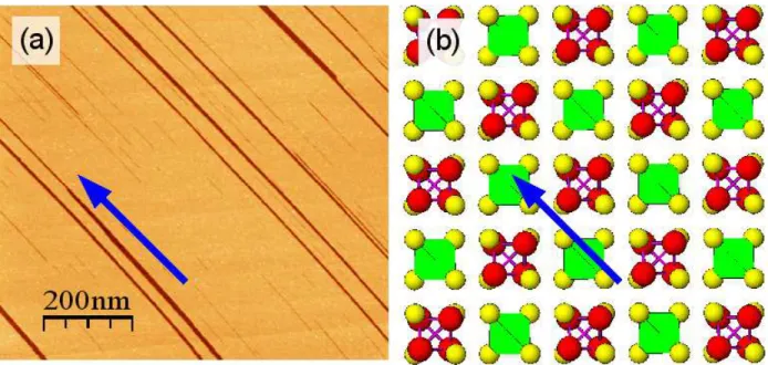
large scale topographic STM images acquired on such in-situ cleaved surfaces display large
terraces, several hundred of nanometers wide (Figure 1a). These terraces are notched by
0.5nm deep trenches of various widths, all aligned in the same direction. The direction of the
Submitted to material[6 ,8] corresponds to a rocksalt-type packing of Ta
4Se16 clusters and GaSe4 tetrahedra,
sharing Se atoms. Hence, a cleavage parallel to (100) likely breaks Ta-Se bonds, exposing a
slab where Ta4Se16 clusters and GaSe4 tetrahedra alternate. The thickness of such a slab is half
the unit cell parameter, i.e. 0.5 nm, that corresponds to the depth of the observed trenches.
The surface space group is p2mm and the direction of the trenches corresponds to the [1-1]
direction, parallel to the rows of GaSe4 tetrahedra and Ta4Se16 clusters (Figure 1b). This kind
of pattern, as well as its close relation to the crystal structure is a strong evidence of an
important surface relaxation[1]. A zoom on an atomically flat terrace is shown Figure 2a.
Despite its disordered appearance, the surface has a very small roughness of typically 100 pm.
The self-correlation analysis allows estimating a characteristic lateral size for the observed
bumps to roughly 3 nm. Despite numerous attempts, atomic resolution imaging has not been
achieved on this surface[2]; spatial inhomogeneities have been observed everywhere on the
surface; their overall pattern is reproducible from one sample to another.
The tunnelling junction was characterized using current versus distance spectroscopy I(Z). As
the tip is retracted, the I(Z) spectra display an exponential decay. Assuming a standard
expression for the tunnelling current I(Z) = exp(-2κZ), where κ =
2m∗W /ℏ and m* = me,one obtains a high work function W = 5.6 +/- 0.2 eV, evidencing a clean vacuum tunneling
junction.
Results and discussion
The influence of voltage pulses was studied in the following manner. First, the tip position
was regulated with a typical current set-point I = 0.1 nA for an applied voltage across the
junction Vbias = 0.7 V. Then, the tip position was fixed by switching off the STM feedback
loop, and a rectangular bias pulse was applied for the desired time. At the end of the pulse, the
bias voltage was switched back to its initial value, and the STM feedback loop was switched
1.1V we systematically observed a sudden saturation of the STM current preamplifier. This is
a clear signature of the appearance of a conducting link between the STM tip and the sample
surface[3]. In order to evaluate the effect of the pulses on the surface, we performed constant
current STM images of the perturbed region with a moderate Vbias~0.7V at which the
tunnelling junction always showed a conventional behaviour. The STM images revealed that
the pulses created nanometre scale craters with a typical depth of 1 to 3 nm, as measured with
respect to the unmodified surface (see Fig 3a). Their inner structure displayed a pattern with a
well reproducible shape that we attributed to the footprint of the tip. This is quite similar to
what Carrasco et al.[9] found in nano-indentation experiments on Au. The periphery of the
crater is roughly circular. Such a peculiar crater shape is consistent with the formation of a
tip-surface nano-contact upon bias pulses.
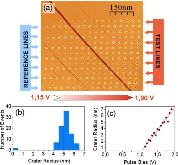
To analyze the effect of voltage pulses on the crater size we applied pulses on a grid varying
both the pulse voltage and duration, as shown in Fig 3. The craters in the test lines (red arrows
in Fig. 3a) were created using 100 µs, 500 µs, 1 ms, 5 ms, 20 ms, 50 ms and 100 ms pulse
duration (from bottom to the top) and pulse voltage varying from +1.15V to +1.9 V by steps
of 0.05 V (from left to right). On the other hand, all the craters of the reference grid lines
(blue arrows in Fig. 3a) were made with identical 100 ms pulses of 1.6V. The reference lines
were thus used to check the reproducibility of the crater creation[4].The size distribution of
the reference craters is surprisingly narrow, as the histogram in Fig.3b shows. One should
note the very low rate of unsuccessful attempts i.e. missing crater (in Fig. 3a), of the order of
2 %. The crater radius distribution nicely follows a Gaussian statistics, with an average radius
of 5.5 nm and a radius variation of about 10 %. Going back to the test lines, it comes directly
from Fig.3a that the pulse amplitude is a relevant parameter in the crater creation, while the
pulse duration does not seem important, at least in the studied range. In Fig. 3c we have
Submitted to
increases linearly with voltage pulse; an extrapolation to zero gives a voltage threshold of 1.1
V for the crater creation. We also checked the influence of the set point (i.e. of the
tip-to-sample distance) on the crater formation. To do so, before applying the voltage pulse, we
moved the tip towards the sample by a controlled distance ranging from 0 to 2 Angstroms
(keeping the feed back loop of the STM open). Within the studied range, we did not observe
any significant dependence of the crater size and shape on the tip-sample distance. We argue
that in the Mott insulator the screening is poor, and the electric field of the tip spreads well
inside the material and consequently, it is not so sensitive to variations of a few Angstroms of
the tip-sample distance. Finally, we studied the influence of the sign of the voltage pulse but
we did not find any significant difference between opposite voltage pulses.
Using the process described above we were able to routinely create thousands of reproducible
10-15 nm wide craters at room temperature. In figure 4 we give an example of such a 10 nm
resolution “writing”. Remarkably, it was impossible to “etch” an entire region with such
voltage pulses, i.e. to create continuous “cratered” regions. In fact, the probability to create a
second crater in the vicinity of an existing one is very low for the separation distances smaller
than 10nm. The origin of this effect is still unknown. Hence, with 100ms@1,6V pulses the
resolving power of such a nano-writing is 10 nm, which corresponds to a density of about 5
TeraDots/inch2. This density can be further increased by optimizing the pulse voltages, the
smallest reproducible craters were created with 1ms@1.2V pulses, giving a typical radius of
1nm. Once created, these patterns are remarkably stable, and appear unmodified at room
temperature for at least one week. Continuous scanning at voltages below the threshold value
(1.1V) does not affect the created structures.
Let us address now the possible mechanisms responsible for the surface nanostructuration. In
fact, the nanoscale modification of surface with a STM tip has been extensively studied in the
models for nanostructuring with STM have been proposed: mechanical contact, field
evaporation, Joule heating, electrochemical reactions. Electrochemical reactions induced by
the electric field of the tip as on SrRuO3, Cuprates, Gold, WSe2, manganites[10] are possible
only in air due to the presence of a thin water film on the surface. In our case however, the
crystals were cleaved under UHV and consequently, the effect should be intrinsic to the clean
surface of GaTa4Se8. The fact that the crater radius does not depend on the pulse duration
while it varies linearly with the voltage pulse seems to exclude thermal effects as a possible
origin. Field evaporation and local fusion[11] have also been proposed as possible origins for
nanostructuring on phase change materials; nevertheless, the voltage threshold for the field
evaporation effect on clean surfaces is of the order of the binding energy which corresponds
to several volts. On silver chalcogenides (Ag2S, Ag2Se), the application of an electric field of
the same order of magnitude as in our case, in STM as well as in nano-bridge geometries, can
generate a hole or a neck.[12] This mechanism involves the displacement of Ag+ ions and is
odd regarding to the sign of the electric field which is not consistent with our results.
Therefore none of the previously proposed mechanisms for nanostructuring the surface with a
STM tip seems to apply in the case of GaTa4Se8. Conversely, all our observations for this
compound are consistent with a mechanical instability of the surface upon the application of a
local electric field. This surface inflation below the tip suggests the existence of an
electromechanical coupling in GaTa4Se8. As the structure of GaTa4Se8 is non centrosymmetric
and compatible with piezoelectricity, a straightforward explanation of this phenomenon could
be a piezoelectric response of the material. However, piezoelectricity is a linear, and hence
odd, relation between the strain and the electric field, which is not consistent with our
experimental findings. At this step it is therefore not yet possible to conclude concerning the
nature of the observed electromechanical coupling in GaTa4Se8. However this finding might
Submitted to
exhibits both a pressure and an electric pulse induced insulator-metal transition. An
electromechanical coupling which would convert the electric field in a kind of “pressure
effect” might therefore be the missing link between the application of an electric pulse and the
modification of the resistance state of GaTa4Se8.[5] In that respect the electro-mechanical
coupling evidenced in our experiments supports a new mechanism of EPIRS phenomenon in
GaTa4Se8 i.e. an electric pulse breakdown of the fragile Mott insulating state of this
compound.
Conclusions
In conclusion, we have demonstrated that the UHV cleaved (100) surface of GaTa4Se8
becomes mechanically unstable upon the application of a local electric field. As a result, short
voltage pulses above the threshold bias Vthershold ~1.1 Volts produce sharp holes at the surface.
This process, which depends neither on sign nor on pulses duration, can be used for
nanostructuring the surface, allowing a pattern density up to 5 TeraDot per inch2 stable at
room temperature. This effect cannot be related to the mechanisms for nanoscale
modifications of the surface reported until now. The most probable origin is linked to the
presence of a strong electro-mechanical coupling in GaTa4Se8. In the near future, conducting
tip Atomic Force Microscopy experiments will allow following the bulging of the surface in a
more direct way. Finally, the observed electro-mechanical coupling might give new clues to
understanding the striking Electric Pulse Induced Resistive Switching recently observed in
this compound.
Experimental
[1] Surface caracterization: At this stage of study, the driving force of this surface relaxation
[2] STM Resolution : Note that our STM set-up has a resolution better than 1pm as determined
by atomic resolution imaging on noble metal surfaces like Silver (111) obtained at room
temperature
[3] Caracterization of the effect : Such a puzzling effect was observed uniquely on AEP
GaTa4Se8 crystals. It was never observed in our STM set-up when studying Ag(111),
Au(111), Si(111), Si(557), Pb/Si, NbSe2, HOPG samples with W, Au, Pt/Ir, Nb tips.
[4] Protocol modification : note that in some experiments we slightly modify the protocol: the
tip was brought 2 Angstroms closer to the surface after switching the feedback loop off. The
only found difference is in the enhanced reproducibility of the crater formation, but not in the
aspect or in the size of the crater
Received: ((will be filled in by the editorial staff)) Revised: ((will be filled in by the editorial staff)) Published online: ((will be filled in by the editorial staff))
_[1] Waser R.; Aono M. Nat. Mat. 2007 6 833-840
_[2] Kim D. C ., Seo S., Ahn S. E., Suh D.-S., Lee M. J., Park B.-H., Yoo I. K., Baek I. G.,
Kim H.-J., Yim E. K., Lee J.E., Park S. O., Kim H. S., Chung U.-I., Moon J. T. and Ryu B. I.,
Appl.Phys. Lett. 2006, 88, 202102
_[3] Liu S. Q., Wu N. J. and Ignatiev A., Appl. Phys. Lett. 2000, 76, 2749
_[4] Szot K., Speier W., Bihlmayer G. and Waser R. , Nat. Mat. 2006, 5, 312-320
_[5] Vaju C., Cario L., Corraze B., Janod E., Dubost V., Cren T., Roditchev D.,
Submitted to
_[6] Abd-Elmeguid M. M., Ni B., Khomskii D. I., Pocha R., Johrendt D . , Wang X. and
Syassen K . , Phys. Rev.Lett. 2004, 93, 126403
_[7] Vaju C., Cario L., Corraze B., Janod E., Dubost V., Cren T., Roditchev D.,
Braithwaite D., Chauvet O., Microelectr. Eng. 2008, 85, 2430.
_[8] Ben Yaich H.; Jegaden J. C.; Potel M.; Sergent M.; Rastogi A. K.; Tournier R.; Jour.
of Less-Com. Met.. 1984 102, 9-22
_[9] Carrasco E.; Gonzalez M. A.; Rodriguez de la Fuente O.; Rojo J. M. Surf. Science
2004, 572 467-475
_[10] You C. C.; Rystad N. V.; Borg A.; Tybell T. Appl. Surf. Science 2007 253
4704-4708, Li R-W.; Kanki T.; Tohyama H-A.; Zhang J.; Tanaka H.; Takagi A.; Matsumoto T.;
Kawai T.J.; Appl. Phys. 2004 95 7091-7093 Fan Y. C.; Fitzgerald A. G.; Cairns J.A.; Journ.
of vac. science and technology B 2000 18 2377-2383 Jaeckel B.; Gassenbauer Y.;
Jaegermann W.; Tomm Y. Surf. Science 2005 597 65-69
_[11] Koning R.; Jusko O.; Koenders L. Journ. of Vac. science and Tech.B 1996 14 48-53
,Chang C. S.; Su W. B.; Tsong T. T. Phys. Rev. Lett. 1994 72 574-577
_[12] Utsigi Y.Nature 1990 347 747-749, Terabe K.; Hasegawa T.; Nakayama T.; Aono M.
Nature 2005 433 47-50
Figure 1. (a) topographic STM image (Vbias = 0.71 V, IT = 0.179 nA) acquired on a cleaved
surface of GaTa4Se8 under Ultra High Vacuum. (b) Crystal structure of the (100) plane of
GaTa4Se8 (Ta atoms: red, Se atoms: yellow, GaSe4 tetraedra: green). The arrows indicate the
Figure 2. (a) Small scale topographic STM image (Vbias = 0.80 V, IT = 0.11 nA) showing
inhomogeneities with a characteristic size of ~3 nm. (b) The topographic profile corresponding to the black line in (a) showing the 1Å typical roughness of the surface.
Submitted to
Figure 3. (a) Topographic STM image (Vbias = 0.71 V, IT = 0.17 nA) showing the effect of
duration and voltage of the pulses. Reference grid lines are made with 100ms@1.6V pulses. The test lines were done by varying the voltage pulse amplitude from 1.15 V to 1.9 V from left to right while the pulse duration varies from 100 µs to 100 ms from bottom to top. (b) Histogram showing the distribution of the crater radii of the reference grid. (c) Dependence of the crater radius as a function of the pulse voltage: Red dots represent the crater radius
averaged with respect to the pulse duration, solid line is a linear fit.
Figure 4. Topographic STM image (Vbias = 0.758 V, IT = 0.186 nA) of a nanostructured
pattern. The dots were done with 100 ms @ 1.6 V pulses. Note that a step of a half the unit-cell height is clearly visible at the top of the image.
The table of contents entryWe report the first experimental evidence for a strong
electromechanical coupling in the Mott insulator GaTa4Se8 allowing a highly reproducible
nano-writing with a Scanning Tunneling Microscope. Above a threshold voltage the surface inflates and comes in contact with the STM tip, resulting in nanometer size craters. These patterns can be indestructibly “read” by STM at lower voltage bias, thus allowing a 5 Tdots/inch2 dense writing/reading at room temperature.
Keywords: Electric field effects, Mott insulator, Surface patterning, Scanning tunneling microscopy, Transition metal chalcogenides.
Vincent Dubost*, Tristan. Cren, Cristian Vaju, Laurent Cario, Benoit Corraze, Etienne Janod, François Debontridder, Dimitri Roditchev
Title : Electric Field Assisted Nanostructuring of a Mott Insulator
Submitted to
Column Title: Vincent Dubost et al./Electric Field Assisted Nanostructuring of a Mott Insulator