HAL Id: tel-01187568
https://hal.archives-ouvertes.fr/tel-01187568
Submitted on 27 Aug 2015HAL is a multi-disciplinary open access archive for the deposit and dissemination of sci-entific research documents, whether they are pub-lished or not. The documents may come from teaching and research institutions in France or abroad, or from public or private research centers.
L’archive ouverte pluridisciplinaire HAL, est destinée au dépôt et à la diffusion de documents scientifiques de niveau recherche, publiés ou non, émanant des établissements d’enseignement et de recherche français ou étrangers, des laboratoires publics ou privés.
Modeling, design and fabrication of diffractive optical
elements based on nanostructures operating beyond the
scalar paraxial domain
Giang Nam Nguyen
To cite this version:
Giang Nam Nguyen. Modeling, design and fabrication of diffractive optical elements based on nanos-tructures operating beyond the scalar paraxial domain. Optics / Photonic. Télécom Bretagne; Uni-versité de Bretagne Occidentale, 2014. English. �tel-01187568�
N° d’ordre : 2014telb0336
Sous le sceau de l
Sous le sceau de l’’Université européenne de BretagneUniversité européenne de Bretagne
Télécom Bretagne
En accréditation conjointe avec l’Ecole Doctorale Sicma
MODELING, DESIGN AND FABRICATION OF
DIFFRACTIVE OPTICAL ELEMENTS BASED ON NANOSTRUCTURES
OPERATING BEYOND THE SCALAR PARAXIAL DOMAIN
Thèse de Doctorat
Mention : Sciences et Technologies de l'Information et de la Communication
Présentée par Giang-Nam Nguyen Département : Optique
Directeur de thèse : Kevin Heggarty Soutenue le 9 décembre 2014
Jury :
M. Pierre Ambs – Prof., Université de Haute-Alsace (Rapporteur) M. Nicolas Guérineau – HDR, ONERA Palaiseau (Rapporteur) M. Kevin Heggarty – Prof., Télécom Bretagne (Directeur de thèse)
M. Patrick Meyrueis – Prof., Université de Strasbourg (Co-directeur de thèse) M. Philippe Gérard – HDR, INSA Strasbourg (Encadrant de thèse)
Modeling, design and fabrication of
diffractive optical elements based on
nanostructures operating beyond the
scalar paraxial domain
Giang-Nam NGUYEN
Acknowledgements
I would like to express my deepest gratitude to my principle advisor, Mr. Kevin Heggarty - Professor at T´el´ecom Bretagne for his excelent guidance, supervision and patience during my doctoral thesis. I would also like to acknowledge Mr. Philippe G´erard - Maˆıtre de conf´erences (HDR) at INSA Strasbourg and Mr. Patrick Meyrueis - Professor at T´el´ecom Physique Strasbourg, for helping me develop my background in diffractive optics and providing me with research directions.
I am grateful to Mr. Andreas Bacher and Mr. Peter-J¨urgen Jakobs for their instruc-tion and support during my stay at Karlsruhe Institute of Technology in Germany for the fabrication of submicron Diffractive Optical Elements using Electron Beam Lithog-raphy. I would also like to thank Mr. Patrice Baldeck - Professor at Joseph Fourier University in Grenoble for his advice during our collaboration in parallel Two-Photon Polymerization lithography.
I would not be able to finish my dissertation without the kind reviewers: Mr. Pierre Ambs - Professor at University of Upper Alsace in Mulhouse, Mr. Nicolas Gu´erineau - Maˆıtre de conf´erences (HDR) at ONERA in Palaiseau and Mr. Pierre-Emmanuel Durand - Maˆıtre de conf´erences at University of South Brittany in Lorient. I am very thankful for their patience in correcting my thesis.
Last but not least, I appreciate the help and fruitful discussions from scientists, staffs and fellow students at T´el´ecom Bretagne, T´el´ecom Physique Strasbourg, Joseph Fourier University and Karlsruhe Institute of Technology. I also thank my family and my friends for their support and encouragement during my doctoral thesis.
My sincere thanks to all of you!
Contents
Acknowledgements i
Table of contents vi
Abbreviations vii
List of figures xiv
List of tables xvi
Abstract xvii
R´esum´e xix
General introduction 1
1. State of the art 7
1.1. Development history of diffraction theory . . . 7
1.2. Review of design algorithms . . . 9
1.2.1. Unidirectional algorithm . . . 10
1.2.2. Bidirectional algorithm . . . 12
1.3. Review of fabrication technology. . . 13
1.3.1. Diamond machining . . . 13
1.3.2. Mask based lithography . . . 14
1.3.3. Parallel direct writing . . . 16
1.3.4. Electron Beam Lithography . . . 17
1.4. Design and experimental requirements . . . 18 iii
iv CONTENTS
1.4.1. Non-pixelated elements . . . 18
1.4.2. Replicated structures . . . 19
1.5. Thesis problem formulation . . . 20
2. Diffraction models 23 2.1. Introduction . . . 23
2.2. DOE region . . . 25
2.2.1. Thin Element Approximation . . . 25
2.2.2. Vectorial theory . . . 26
2.3. Free-space propagation region . . . 29
2.3.1. From vectorial to scalar theory . . . 29
2.3.2. The Angular Spetrum Method . . . 29
2.3.3. The Rayleigh-Sommerfeld diffraction formula. . . 32
2.3.4. The scalar paraxial approximation . . . 34
2.3.5. The scalar paraxial approximation in the far field . . . 37
2.3.6. Repeated propagation method . . . 38
2.3.7. Comparison of different free-space propagation methods. . . 40
2.4. Conclusion . . . 41
3. Scalar theory for the modeling and design of DOEs operating in the non-paraxial far-field diffraction regime 43 3.1. Proposed scalar non-paraxial method . . . 43
3.1.1. Hemisphere-to-plane projection . . . 45
3.1.2. Resampling from angular to spatial coordinates . . . 47
3.1.3. The diffraction position. . . 47
3.1.4. The diffracted power . . . 47
3.1.5. Computer simulations and discussions . . . 49
3.1.6. Summary of scalar non-paraxial far-field method . . . 54
3.2. Iterative scalar non-paraxial algorithms for Fourier elements . . . 55
3.2.1. Limit of the iterative scalar paraxial design. . . 55
3.2.2. Single projection . . . 56
3.2.3. Iterative projection . . . 58
CONTENTS v
3.3. Conclusion . . . 61
4. Vectorial theory for the modeling and design of DOEs operating in the non-paraxial far-field diffraction regime 63 4.1. Limit of the Thin Element Approximation . . . 64
4.1.1. The diffracted electromagnetic components . . . 64
4.1.2. Symmetry of the far-field diffraction pattern of binary elements 67 4.1.3. Summary of our TEA investigation . . . 71
4.2. Rigorous vectorial model . . . 72
4.2.1. FDTD spatial resolution . . . 73
4.2.2. FDTD propagation distance . . . 73
4.2.3. FDTD simulation time . . . 74
4.2.4. Coupling resolution . . . 75
4.2.5. 2D simulation and FDTD parallelization . . . 76
4.2.6. Summary of our rigorous vectorial model . . . 79
4.3. Genetic algorithm for the design of thick DOEs . . . 80
4.4. Conclusion . . . 81
5. Experimental verification and effects of fabrication errors on the ex-perimentally observed diffraction pattern 83 5.1. Introduction . . . 83
5.1.1. DOE fabrication at TB . . . 84
5.1.2. DOE fabrication at KIT . . . 85
5.2. Experimental verification of the scalar non-paraxial model and design algorithms . . . 86
5.2.1. Scalar non-paraxial modeling . . . 86
5.2.2. Iterative scalar non-paraxial design . . . 90
5.3. Effects of fabrication errors and the limit of the TEA on the experimental diffraction symmetry . . . 93
5.3.1. Effects of fabrication errors . . . 93
5.3.2. Limit of the TEA . . . 97
5.4. Example DOE applications. . . 99
5.4.1. Rectangular pattern . . . 99
vi CONTENTS
5.4.3. Spot array DOEs . . . 101
5.5. Conclusion . . . 103
6. Parallel two-photon polymerization lithography 105 6.1. Review of 2PP lithography . . . 105
6.1.1. Principle of 2PP . . . 105
6.1.2. Current parallel 2PP systems . . . 108
6.2. Experimental 2PP photoplotter . . . 109
6.3. Preliminary fabrication results . . . 112
6.3.1. Gold ablation . . . 112
6.3.2. 2PP fabrication . . . 114
7. Conclusion and perspectives 117 Sommaire 119 Appendix A. Two-step propagation 129 A.1. Scaled Fresnel . . . 129
A.2. Scaled paraxial ASM . . . 130
A.3. Cascaded aperture effect . . . 131
Appendix B. Diffracted power estimation 133 B.1. Vectorial theory . . . 133
B.2. Scalar theory . . . 134
Appendix C. Boundary conditions 135 C.1. Perfectly Conducting Boundary . . . 135
C.2. Floquet-Bloch Periodic Boundary . . . 135
C.3. Perfect Matched Layer . . . 136
Abbreviations
AFM Atomic Force Microscope ASM Angular Spectrum Method
BS Beam Splitter
CCD Charge-Coupled Device
CD Compact Disc
CGH Computer Generated Hologram DBS Direct Binary Search
DOE Diffractive Optical Elements DVD Digital Video Disc
EBL Electron Beam Lithography FDTD Finite-Difference Time-Domain FMM Fourier Modal Method
FT Fourier Transform GA Genetic Algorithm
IASA Iterative Angular Spectrum Algorithm
Ifremer Institut Fran¸cais de Recherche pour l’Exploitation de la Mer IFT Inverse Fourier Transform
IFTA Iterative Fourier Transform Algorithm JFU Joseph Fourier University
KIT Karlsruhe Institute of Technology LCD Liquid Crystal Display
MEEP MIT Electromagnetic Equation Propagation MPI Message Passing Interface
MSE Mean-Square Error NA Numerical Aperture OPD Optical Path Difference
ORMOCER ORganically MOdified CERamic
PC Personal Computer
PI Physik Instrumente PMMA Poly-methyl methacrylate
viii ABBREVIATIONS
RAM Random-Access Memory
RCWA Rigorous Coupled-Wave Analysis RIE Reactive-Ion Etching
RoD Ratio of Difference RMSE Root-Mean-Square Error RS Rayleigh-Sommerfeld
RSM Radiation Spectrum Method SLM Spatial Light Modulator TB T´el´ecom Bretagne TI Texas Instruments TE Tranverse Electric
TEA Thin Element Approximation TM Tranverse Magnetic
TPS T´el´ecom Physique Strasbourg
1D 1-Dimensional
2D 2-Dimensional
2PP 2-Photon Polymerization
List of Figures
1. Output patterns of example DOEs (a) A spot array (for beam splitting applications). (b) A grid pattern (for machine vision applications). . . 4
1.1. Diffraction geometry. . . 9
1.2. Continuous thickness profile of a blazed grating, and a 4-level quantized profile. . . 9
1.3. Unidirectional algorithm flowchart. . . 11
1.4. (a) Stagnation effect where the design algorithm stops at a local opti-mum. (b) Convergence to the global optiopti-mum. . . 12
1.5. Bidirectional algorithm flowchart. . . 13
1.6. (a) Mechanical ruling of a blazed grating using a diamond tip adapted to grating geometry. (b) Diamond turning of a microlens. . . 14
1.7. Basic procedure of binary DOE fabrication process using mask based lithography. . . 15
1.8. Basic procedure of 2L level DOE fabrication process using mask based lithography. . . 15
1.9. (a) Basic procedure of direct laser writing. (b) Principle of parallel direct-write lithography at TB. . . 16
1.10. (a) Basic procedure of EBL. (b) An electron beam writer, which is a Vistec VB6 UHR-EWF (Ultra High Resolution-Extra Wide Field, photo courtesy of the KIT). . . 18
1.11. Several configurations of possible DOE illumination. . . 19
1.12. Diffraction pattern of a spot array DOE: (a) with and (b) without speckle effect. . . 20
2.1. Two-dimensional diffraction geometry, with the problem divided into different regions, where U stands for both the electric and magnetic fields. 24
x LIST OF FIGURES
2.2. Propagation of two light rays through a L level phase DOE in the TEA. 26
2.3. Yee grid and leap-frog time steps. . . 27
2.4. The wave propagation direction. . . 30
2.5. Diffraction geometry. . . 32
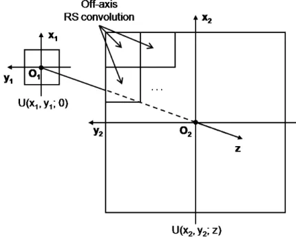
2.6. Principle of a repeated calculation based on off-axis RS convolution. . . 39
2.7. Two-step propagation geometry. . . 40
3.1. Diffraction geometry of the Harvey model. . . 44
3.2. (a) The diverging effect from the hemisphere to the observation plane. (b) Multiradii approach. . . 46
3.3. Diffraction power estimation. . . 48
3.4. (a) Target image, which is a 256×256 pixel image at diffraction distance of 18 cm, spot separation of about 3.5 cm. (b) Fourier DOE designed by an IFTA, where a period is 8 µm. . . 49
3.5. Ratio of difference to the RS calculated diffraction pattern for the ob-servation plane diffraction patterns calculated using: (a) Angular Fraun-hofer approximation. (b) Harvey method plus plane wave projection. (c) Harvey method plus spherical wave projection. . . 50
3.6. Comparison between the simulated diffraction patterns of the test DOE obtained by using: (a) RS convolution, (b) ASM, (c) RS integral, (d) Fraunhofer approximation, (e) Angular Fraunhofer approximation with nonlinear mapping, (f) Multiradii approach. Due to the sampling con-straint, the RS convolution and the ASM only obtain a small area around the optical axis. . . 51
3.7. Zoomed images of the top left corner of the simulated diffraction patterns obtained by using: (a) RS integral, (b) Fraunhofer approximation, (c) Angular Fraunhofer approximation with nearest-neighbor interpolation, (d) Multiradii approach with nearest-neighbor interpolation, (e) Angu-lar Fraunhofer approximation with bilinear interpolation, (d) Multiradii approach with bilinear interpolation. . . 53
3.8. (a) Desired output pattern. (b) Reconstruction pattern of a DOE de-signed using the standard IFTA. . . 56
3.9. Non-paraxial Fourier DOE design algorithm using single projection from the output plane to the hemisphere and IFTA between the hemisphere and the DOE plane. . . 56
LIST OF FIGURES xi
3.10. Non-paraxial Fourier DOE design algorithm using single projection from the output plane to the hemisphere and IFTA between the hemisphere and the DOE plane. . . 57
3.11. (a) Projection of the grid pattern on the hemisphere using nearest-neighbor interpolation. (b) Reconstruction pattern of the DOE designed using single projection with nearest-neighbor interpolation. (c) Zoomed image of the top left corner of the pattern in (b). (d) Reconstruction pattern of the DOE designed using single projection with bicubic inter-polation. . . 58
3.12. Non-paraxial Fourier DOE design algorithm using iterative projection between the output plane and the hemisphere and IFTA between the hemisphere and the DOE plane. . . 59
3.13. (a) Reconstruction pattern of a DOE designed at δ1 = 400 nm using
iterative projection with bicubic interpolation. (b) Zoomed image of the top left corner of the pattern in (a). . . 59
3.14. Reconstruction pattern of the DOEs designed at δ1 = 300 nm using (a)
standard IFTA, (b) iterative projection with bicubic interpolation. . . . 60
4.1. FDTD simulation (MEEP) of a periodic 1D binary grating illuminated by a linear s-polarized plane wave and the diffracted fields. (a) One period of the grating structure and the illumination field. (b) Ey. (c)
Hx. (d) Hz. . . 65
4.2. The state of Hz obtained by the FDTD simulation (MEEP): (a) after
4.5 optical cycles, and (b) after 6 optical cycles. . . 66
4.3. Normalized amplitude (a) and phase (b) of the diffracted field imme-diately after the grating. The results were obtained using the TEA (Ey· exp{jφ(x)}) in comparison with the FDTD simulation (MEEP). . 66
4.4. (a) A period of an asymmetrical binary Fourier DOE. (b) A period of a symmetrical binary Fourier DOE, where the dashed line is the reflection symmetry axis. (c) Target image. . . 68
4.5. Average Hermitian symmetry factor at different DOE feature sizes. FMM simulations of DOEs having feature sizes larger than 2.5 µm were not possible due to the limited amount of computing memory available (16 GByte of RAM). . . 69
4.6. (a) A binary grating with T = 4 µm and f = 0.25, where the dashed line is the reflection symmetry axis. (b) The angular diffraction pattern of the grating simulated using FMM in VirtualLabT M (λ = 1 µm, linear
xii LIST OF FIGURES
4.7. Simulated diffraction efficiency of the coupling model at different FDTD spatial sampling resolutions: (a) The FMM (LightTrans VirtualLabT M).
(b) The TEA + Harvey model. (c) The FDTD + Harvey model. . . 72
4.8. Simulated diffraction efficiency of the coupling model at different FDTD spatial sampling resolutions: (a) 0th order, (b) 1st order. . . . . 74
4.9. Contribution of the spherical waves from the neighboring periods to the simulation region. . . 75
4.10. Simulated diffraction efficiency of the coupling model at different FDTD simulation times: (a) 0th order, (b) 1st order. . . . . 75
4.11. The surface area of the diffraction order on the hemisphere.. . . 77
4.12. Effect of super-computer parallelization on the simulation time. . . 79
4.13. (a) A binary phase element. (b) Complementary element. (c) Additi-tional 2π phase shift elements. . . 80
4.14. Genetic algorithm for the design of binary thick DOEs. . . 81
5.1. (a) DOE fabrication procedure in the TB cleanroom. (b) Spin-coater. (c) Parallel direct-write photoplotter. (d) Interferometric microscope. (e) Optical setup for DOE characterization. . . 84
5.2. (a) DOE fabrication procedure using EBL. (b) Electron beam writer. (c) RIE cluster, including a Oxford RIE Plasmalab System 100. (d) An AFM. (Photo courtesy of the KIT) . . . 86
5.3. (a) Optical interferometric microscope image of the fabricated DOE, where a period is about 8 µm. (b) Optical DOE playback setup. . . 87
5.4. Superposition of the simulated and experimental diffraction patterns. The green spots are those predicted by the multiradii Harvey calculation, whereas the red spots are those of the experimentally observed pattern. The yellow regions are where they overlap. . . 88
5.5. The effect of exposure time to the etch profile and pixel linewidth. . . . 89
5.6. (a) AFM image of the test DOE. (b) Etching profile of the test DOE, where the edges look slanted due to the size of the tip used for AFM measurement. . . 90
5.7. Experimental patterns of the DOEs designed at δ1 = 400 nm using: (a)
Standard paraxial IFTA, (b) Non-paraxial IFTA with single projection + nearest neighbor interpolation, (c) Non-paraxial IFTA with single projection + bicubic interpolation, (d) Non-paraxial IFTA with iterative projection + bicubic interpolation. . . 91
LIST OF FIGURES xiii
5.8. (a) Zoomed image of the top left corner of the pattern in 5.7(b). (b) Zoomed image of the top left corner of the pattern in 5.7(d). . . 91
5.9. Experimentally observed patterns of the 300 nm feature size DOEs de-signed using: (a) Standard paraxial IFTA, (b) Non-paraxial IFTA with iterative projection + bicubic interpolation. . . 92
5.10. (a) A symmetrical binary Fourier DOE, where the dashed line is the reflection symmetry axis. (b) An asymmetrical binary Fourier DOE. (c) Target image. . . 94
5.11. Different models for the DOE structure: (a) Flawless model, (b) Trape-zoid model, (c) Rounding model. . . 96
5.12. (a) and (b) Interferometric microscope images of the DOEs fabricated using our current photoplotter at 2 µm and 1 µm, respectively. (c) AFM image of the DOE fabricated at 500 nm using EBL at KIT. . . 98
5.13. (a) Desired diffraction pattern. (b) Experimentally observed pattern of the DOE designed using the iterative scalar paraxial algorithm and fab-ricated at 1 µm feature size using our photoplotter. . . 100
5.14. (a) The DOE designed using the iterative scalar paraxial algorithm at 500 nm feature size. (b) Experimentally observed pattern of the DOE fabricated using our photoplotter. . . 100
5.15. (a) 3D interferometric microscope image of a 8 level blazed grating. (b) Etching profile of the structure in (a). . . 101
5.16. Experimentally observed diffraction patterns of the fabricated DOEs: (a) 25×25 spot array, (b) 47×47 spot array. . . 102
5.17. (a) Intensity distribution over a horizontal line across the zero order of the 25×25 spot array. (b) Microscope image of the parallel 2PP fabrica-tion using our 25×25 spot array DOE. . . 103
6.1. (a) One-photon absorption. (b) Two-photon absorption. (c) 2PP in the photoresist layer and at the focal spot of a focusing beam. (ν is the frequency of the write-beam and h is the Planck constant) . . . 106
6.2. (a) Intensity distribution of a focused beam in the axial and lateral directions. (b) Axial and lateral resolutions of the 2PP voxel. . . 107
6.3. (a) Gaussian and squared gaussian intensity profile. (b) Threshold power relative to various gaussian intensity profiles. The closer the peak power to the threshold power, the smaller the voxel size. 2PP is not observed if peak power is below the threshold power.. . . 108
xiv LIST OF FIGURES
6.5. Simulated 2PP voxel size with different microscope objective using a software developed by JFU: (a) 0.7 µm lateral and 8.8 µm axial res-olutions for the 20X objective, (b) 0.3 µm lateral and 0.7 µm axial resolutions for 100X objective. . . 111
6.6. CCD camera images when the focus is (a) at the air-substrate interface and (b) at the substrate-photoresist interface. In the latter case, the image had more rings than that of the air-glass interface focusing. . . . 111
6.7. Optical setup of the parallel 2PP photoplotter in TB cleanroom. . . 112
6.8. Microscope image of a pattern fabricated by sequential gold ablation. The white regions are the ablated areas. . . 113
6.9. Microscope images of the patterns fabricated by parallel gold ablation using a 40X microscope and: (a) 1 pulse, (b) 10000 pulses, (c) 50000 pulses, (d) 100000 pulses. The black regions are the ablated areas. . . . 114
6.10. Microscope images of different lines fabricated by sequential 2PP. Each vertical line corresponds to a laser power going into the microscope ob-jective. From left to right is the direction of reducing laser power. . . . 115
7.1. Structure g´eom´etrique de la diffraction dans le mod`ele de Harvey et notre projection d’onde sph´erique. . . 121
7.2. (a) Algorithme it´eratif utilisant une seule projection. (b) Algorithme It´eratif utilisant une projection it´erative. . . 123
List of Tables
2.1. Simulation constraints and validity regions of different diffraction models for the free-space propagation. . . 41
3.1. Simulated diffraction angles and efficiencies of sample diffraction orders calculated by different methods. The RS convolution and the ASM are not shown as they are inapplicable to calculate the entire output field due to sampling constraint. . . 53
3.2. Comparison between the performance of different design algorithms (af-ter 110 i(af-terations). . . 60
4.1. Simulated diffraction efficiency (%) of diffraction orders (m, n) of the asymmetrical DOE using: (a) the TEA + our free-space propagator and (b) the FMM (LightTrans VirtualLabT M). . . . . 68
4.2. Simulated diffraction efficiency (%) of diffraction orders (m, n) of the symmetrical DOE with spherical polarization illumination using the FMM (LightTrans VirtualLabT M). . . . . 70
4.3. Diffraction efficiency (%) of different diffraction orders of the grating using different simulation methods. . . 73
4.4. Diffraction efficiency (%) of different diffraction orders of the grating using the FDTD + Harvey model at different distances from the grating surface . . . 74
4.5. Diffraction efficiency (%) of different diffraction orders of the grating using the FDTD + Harvey model at different scaling factors . . . 76
4.6. Simulated diffraction efficiency (%) of diffraction orders (m, n) of the asymmetrical DOE using: (a) the FMM (LightTrans VirtualLabT M) and
(b) the FDTD + Harvey model. . . 77
5.1. Experimentally observed diffraction efficiencies for sample diffraction or-ders of the test DOE with fabrication errors. . . 89
xvi LIST OF TABLES
5.2. Simulated diffraction efficiencies for sample diffraction orders of the test DOE without and with fabrication errors. . . 89
5.3. Diffraction efficiency (%) of diffraction orders (m, n) for the symmetrical binary DOE: (a) Experimental diffraction efficiencies of the diffraction orders for the DOE fabricated using our photoplotter. (b) TEA + our scalar non-paraxial simulation, assuming flawless binary DOE structure. 95
5.4. MSE between the experimental diffraction efficiencies and the TEA + our scalar non-paraxial simulation results of different DOE structure models. . . 97
5.5. Diffraction efficiency (%) of diffraction orders (m, n) for the asymmetric binary phase DOE. (a) Experimental results of the DOE fabricated using EBL. (b) FDTD + Harvey simulation results. . . 98
Abstract
This thesis aims to extend the range of Diffractive Optical Element (DOE) appli-cations by developing models, algorithms and rapid prototyping techniques for DOEs with diffraction angles > 10◦, which is beyond the limits of scalar paraxial diffraction model. We develop an accurate and efficient scalar non-paraxial far-field propagator to overcome the limits of the conventional scalar diffraction models. An iterative algo-rithm based on this propagator is then developed for the design of wide-angle Fourier elements. Experimental results confirm that our scalar non-paraxial propagator and design algorithm can be used for the modeling and design of thin Fourier DOEs with diffraction angles up to about 37◦ and perhaps even higher.
The remaining discrepancies in diffracted power between modeling, design and ex-periment are then shown to result from both fabrication errors and by the fact that we are approaching the limit of the Thin Element Approximation (TEA). The practical limits of the TEA are investigated by comparison with the rigorous vectorial simu-lations. We then develop, optimize and parallelize a rigorous diffraction model based on the Finite-Difference Time-Domain method coupled with our scalar non-paraxial propagator to overcome the limits of the TEA and the computational limitations of current vectorial models. A genetic design algorithm based on this model is proposed for the design of thick DOEs and this algorithm is currently being calibrated.
These models and algorithms have now brought us to the resolution limit of our ex-isting photoplotter used for DOE fabrication. Therefore, we investigate the possibility of building a new parallel photoplotter based on Two-Photon Polymerization (2PP) as a way to rapid, cost-effective prototyping of high resolution (submicron) structures. We design and fabricate spot array DOEs at T´el´ecom Bretagne to parallelize the 2PP fabrication process used at Joseph Fourier University in Grenoble by a factor of 625. To further speed up the 2PP fabrication process, another prototype parallel 2PP pho-toplotter using a Spatial Light Modulator, which can generate up to about 0.5 million parallel beams, is designed and is currently being developed at T´el´ecom Bretagne.
Keywords : diffraction, scalar non-paraxial, vectorial modeling, design and fabri-cation, parallel 2PP.
R´
esum´
e
Cette th`ese vise `a ´elargir l’´eventail des applications des Elements Optiques Diffrac-tifs (EODs) en d´eveloppant des models, des algorithmes et des techniques de prototy-page rapide pour des EODs avec des angles de diffraction > 10◦, au del`a des limites du model scalaire, paraxiale de diffraction. Nous d´eveloppons un propagateur non-paraxiale scalaire en champ lointain pr´ecis et efficace pour surmonter les limites des mod`eles classiques de la diffraction scalaire. Un algorithme it´eratif bas´e sur ce propa-gateur est d´evelopp´e pour la conception d’´el´ements de Fourier `a grand angle de diffrac-tion. Les r´esultats exp´erimentaux confirment que notre propagateur et notre algorithme scalaire, non-paraxiale peuvent ˆetre utilis´es pour la mod´elisation et la conception des EODs minces avec angles de diffraction jusqu’`a environ 37◦ et peut-ˆetre encore plus ´
elev´e.
Nous montrons que les divergences qui subsistent entre la mod´elisation et l’exp´erimentation de la puissance diffract´ee r´esultent surtout des erreurs de fabrica-tion et par le fait que nous nous approchons de la limite de l’approximafabrica-tion d’un ´
el´ement mince (TEA - “Thin Element Approximation”). Les limites pratiques de la TEA sont ´etudi´ees en comparaison avec le simulations rigoureuses vectorielles. Nous d´eveloppons, optimisons et parall´elisons un mod`ele de diffraction rigoureuse bas´ee sur la FDTD (“Finite-Difference Time-Domain”) coupl´ee avec notre propagateur non-paraxiale scalaire pour surmonter les limites de la TEA et les limites de calcul des mod`eles vectoriels actuels. Un algorithme de conception g´en´etique sur la base de ce mod`ele est propos´e pour la conception des EODs “´epaisses”, il est actuellement en cours d’´etalonnage.
Ces mod`eles et algorithmes nous ont maintenant conduits `a la limite de r´esolution de notre photoplotter existant utilis´e pour la fabrication des EODs. Nous ´etudions la possibilit´e de construire un nouveau photoplotter parall`ele bas´e sur polym´erisation `a deux photons (2PP) comme un moyen de prototypage rapide et rentable de structures haute r´esolution (submicroniques). Nous concevons et fabriquons `a T´el´ecom Bretagne, des EODs generant une matrice de points lumineux pour parall´eliser le processus de fabrication 2PP utilis´e `a l’Universit´e Joseph Fourier de Grenoble par un facteur de 625. Pour acc´el´erer encore le processus de fabrication 2PP, nous concevons et assemblons
xx R ´ESUM ´E
un autre photoplotter 2PP parall`ele `a base d’un modulateur spatial de lumi`ere, qui permet de g´en´erer jusqu’`a environ 0,5 million de faisceaux parall`eles. Ce phototracer est actuellement en cours de d´eveloppement `a T´el´ecom Bretagne.
Mots-cl´es: diffraction, scalaire non-paraxiale, mod´elisation vectorielle, conception et fabrication, 2PP parall`ele.
General introduction
Diffractive Optical Elements (DOEs) are increasingly being used for a broad range of applications [1]. Example DOE applications are beam shapers (for laser welding, cutting, machining), beam splitters (for optical telecommunications couplers), optical disc read-heads (in CD, DVD, Blu-ray), pattern generators (for machine vision) and anti-fraud protection (for security documents), etc. However, traditional theory, which is the scalar paraxial diffraction model, is only valid for the modeling and design of small diffraction angle and thin DOEs. Fabrication technology using high performance facilities now enables manufacturing of wide diffraction angle or thick DOEs, leading to the need for new modeling and design algorithms.
Optical diffraction is a physical phenomenon which occurs when a light beam en-counters an obstacle and propagates in many different directions. The smaller the obstacle, the larger the diffraction angles and the stronger the diffraction effects be-come [2]. Unlike reflection and refraction which can be explained by the corpuscular nature of light (i.e. geometrical optics), diffraction can be best described by the wave nature of light (i.e. electromagnetic theory). The propagation of the diffracted wave can be considered as the interference of Huygens-Fresnel secondary wave sources generated by every point in the obstacle [3]. These waves are superposed together, creating a diffraction pattern with a series of maxima and minima on the observing screen.
DOEs are micro or nanostructures which are designed to modify the spatial distri-bution of a light beam to generate any desired pattern. DOEs can be categorized into different types based on different criteria:
• Depending on how the light beam is modified:
– Amplitude element: the amplitude of light is modulated according to the absorption inside the structure. As part of the light beam is absorbed, this type of DOE has low performance in terms of diffraction efficiency [4]. – Phase element: the light propagates without absorption, only with a
mod-ulated phase according to the phase shift introduced by the structure. • Depending on where the diffraction pattern is observed:
2 GENERAL INTRODUCTION
– Fourier element: the diffraction pattern is observed at the far-field (typi-cally on the order of decimeters beyond the DOE). This type of DOE is usu-ally a diverging element, e.g. beam splitter, beam shaper, where the diffrac-tion pattern is larger than the DOE size.
– Fresnel element: the diffraction pattern is observed at the near-field (typi-cally on the order of millimeters). This type of DOE is usually a converging element, e.g. microlens, where the diffraction pattern is smaller than the DOE size.
• Depending on the observation direction of the diffraction pattern – Transmissive element: the diffraction pattern is observed at the opposite
direction with the light source.
– Reflective element: the diffraction pattern is observed at the same direction with the light source.
• Depending on the DOE thickness compared to the wavelength of light: – Thin element: the DOE thickness is equivalent to a phase shift equal to or
smaller than 2π.
– Thick element: the DOE thickness is equivalent to a phase shift significantly bigger than 2π.
Given a DOE structure, there are various diffraction models which allow the diffrac-tion pattern to be calculated. This is the forward problem, or the modeling process, in which diffraction theory often cannot be solved analytically, but can yield numerical solutions with some simulation constraints and validity regions. These models can be categorized depending on how the electromagnetic field is treated:
• Scalar theory: only one component (E or H) of the electromagnetic field is calculated. Scalar theory is usually used for thin elements, and can be further classified into:
– Scalar paraxial models: a paraxial approximation is used in calculating the amplitude of the diffracted field. This is the traditional diffraction theory, which is only valid for small diffraction angles.
– Scalar non-paraxial models: the amplitude of the diffracted field is calcu-lated rigorously within the scalar domain.
• Vectorial theory: all electromagnetic components of the diffracted field are cal-culated. This is generally required for sub-wavelength DOEs and thick elements.
GENERAL INTRODUCTION 3
More interestingly, from a practical applications viewpoint, the inverse diffraction problem is to create a DOE structure that will produce, by diffraction, a desired target wavefront. This is the DOE design and fabrication process, which generally consists of 3 steps [3]. First, the target image is put into a design algorithm to create a Computer Generated Hologram (CGH). This hologram is then fabricated as a DOE. Finally, the optical function and performance of the DOE are verified experimentally on an optical bench. Traditionally, the CGH has an analog (continuous) profile which is difficult to fabricate accurately, leading to an experimental DOE performance significantly lower than the performance in simulation. For this practical reason, the CGH is often quan-tized into a digital profile with limited numbers of levels (e.g. 2, 4, 8, . . . levels) which are easier to fabricate and result in an experimental DOE performance almost the same as in simulation. However, due to the abrupt analog-to-digital conversion, the quantization process often reduces the CGH performance in simulation [5]. Therefore, an optimization algorithm (e.g. iterative transform [6,7] or genetic algorithm [8,9]) is necessary to select the CGH with the best performance from all possible set of discrete levels. In summary, to design a digital DOE, a mathematical model for the propagation of the diffracted wave has to be chosen, and an optimization algorithm based on this model is developed.
Motivation
This thesis aims to design, build and optimise DOEs operating in more complex diffraction regimes than scalar paraxial theory, with a view to obtaining higher per-formance components (improved diffraction efficiency, larger diffraction angles, new wavelengths, . . . ) and in this way address applications which are for the moment in-accessible. Example applications are DOEs in integrated optics [10], where the devices are becoming more and more compact, which requires DOEs with large diffraction angles. The model design - fabrication - experimental results - feedback used in this thesis allows us to optimize the new complex diffraction regime DOE algorithms and to determine their practical applicability domains in concrete examples. In this way we go beyond the present limitations and make possible the design and fabrication of new families of DOEs for a wider range of applications: wide angle diffraction Fourier DOEs. The practical applications indicated in the thesis were chosen in close collab-oration with the industrial partners of T´el´ecom Bretagne (TB) and of its “start-up” company, Holotetrix, specialised in the commercialisation of DOE prototypes and small series production.
In this work, we focus on digital Fourier phase DOEs, as most of the applica-tions addressed at TB use elements of this type. More specifically, in the preliminary chapters, we will model and design test DOEs producing a diffracted output pattern
4 GENERAL INTRODUCTION
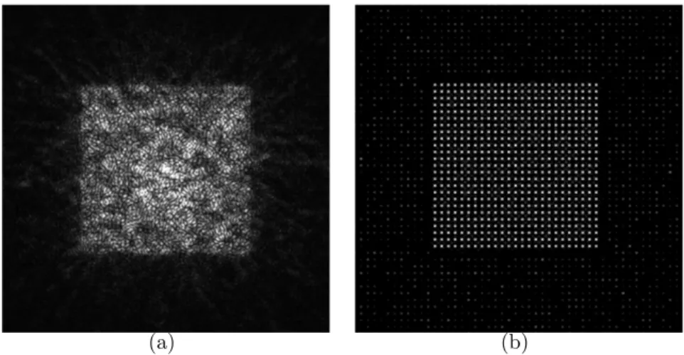
that can be easily measured and tested, have practical applications and exploit a two-dimensional output field (much work has already been performed on vectorial theory modeled DOEs producing one-dimensional output fields but there are few publications with more complex output patterns). Two examples are a 5x5 spot array and a grid pattern shown in Fig. 1, in which the spot array will be useful for the verification of diffraction efficiency, whereas the grid pattern will be helpful for the verification of diffraction pattern distortion at high diffraction angles.
(a) (b)
Figure 1 — Output patterns of example DOEs (a) A spot array (for beam splitting applications). (b) A grid pattern (for machine vision applications).
Organisation of the thesis
With respect to the content of this PhD research, the thesis will be organized as follows. Chapter 1 shortly reviews the development history of diffractive optics, in-cluding the modeling, design and current fabrication technologies. This chapter also briefly introduces the issues that this thesis attempts to answer, i.e. identifying the limitations of different diffraction models, development of efficient algorithms and new optical lithographic system for the modeling, design and fabrication of high perfor-mance DOEs. These issues are further explained in Chapter 2, which analyses in detail the limits of current diffraction theories for the modeling and design of thin and thick elements. For the modeling and design of thin elements, Chapter 3 proposes a scalar non-paraxial propagator and iterative design algorithms based on this model. Chapter 4 presents a vectorial model and a genetic algorithm to overcome the limit of scalar theory in the modeling and design of thick elements. The diffraction models and design algorithms given in these two chapters are verified experimentally in Chapter 5. With these models, we have reached the limit of our fabrication facilities and therefore, some studies on the effects of fabrication limitations on the experimentally observed diffrac-tion pattern are also included in this chapter. To overcome the limits of our current parallel direct-write optical photolithographic system, a new photoplotter based on
GENERAL INTRODUCTION 5
parallel Two-Photon Polymerization (2PP) has been built and is described in Chapter 6. Finally, Chapter 7 concludes the results of this work and proposes some directions for the future.
Thesis contributions
• Analysis of the validity regions and computational constraints of different diffrac-tion models in the scalar paraxial, scalar non-paraxial and vectorial regimes. • Identification of the practical validity of the scalar paraxial regime by the
fabri-cation of test DOEs and the characterisation of their optical performance on an optical bench.
• Development of DOE modeling and design algorithms in the scalar non-paraxial regime. Optimization (design - fabrication - feedback) of each algorithm based on the experimental results.
• Design and fabrication of submicron DOEs (down to 300 nm) where the diffraction angle is up to about 37◦. The DOEs were designed using our scalar non-paraxial algorithm and fabricated using Electron Beam Lithography at Karlsruhe Institute of Technology in Germany.
• Investigation of the limits of the Thin Element Approximation by fabricating test binary DOEs and measuring the Hermitian symmetry of their diffraction patterns on the optical bench.
• Development and optimization of a rigorous vectorial diffraction method for the modeling of thick DOEs. Parallelization of the algorithm on a super-computer. • Study the effects of fabrication errors to the experimental diffraction efficiency and
the symmetry of the diffraction pattern.
• Preliminary development of parallel 2PP as a new fabrication technique for rapid fabrication of high resolution (submicron) large diffraction angle DOEs.
List of publications:
• Journals:
1. G. N. Nguyen, K. Heggarty, P. G´erard, B. Serio, and P. Meyrueis, “Compu-tationally efficient scalar non-paraxial modelling of optical wave propagation in the far-field”, Applied Optics, Vol. 53, Issue 10, pp. 2196-2205, Mar. 2014.
6 GENERAL INTRODUCTION
2. G. N. Nguyen, K. Heggarty, A. Bacher, P. J. Jakobs, D. H¨aringer, P. G´erard, P. Pfeiffer, and P. Meyrueis, “Iterative scalar non-paraxial algorithm for the design of Fourier phase elements”, Optics Letters, Vol. 39, Issue 19, pp. 5551-5554, Sept. 2014.
3. G. N. Nguyen, K. Heggarty, K. Chikha, P. G´erard, and P. Meyrueis, “Diffrac-tion symmetry of binary Fourier elements with feature sizes on the order of the illumination wavelength and effect of fabrication errors”, in preparation. 4. A. Liu, G. N. Nguyen, K. Heggarty, and P. Baldeck, “Fabrication of microscale medical devices by parallel two-photon polymerization using Dammann grat-ings”, in preparation.
• Conferences:
1. G. N. Nguyen, K. Heggarty, P. G´erard, and P. Meyrueis, “Modelling, design and fabrication of diffractive optical elements based on nanostructures op-erating beyond the paraxial scalar regime ” (Poster presentation), Journ´ee Futur & Ruptures, 24 Jan., Paris, France, 2013.
2. G. N. Nguyen, K. Heggarty, P. G´erard, and P. Meyrueis, “Iterative scalar algorithm for the rapid design of wide-angle diffraction Fourier elements” (Oral presentation), EOSMOC 2013: 3rd EOS Conference on Manufacturing of Optical Components, 13-15 May, Munich, Germany, 2013.
CHAPTER
1
State of the art
In this chapter, the historical development of diffractive optics is quickly reviewed. A brief overview of current fabrication technologies is also included. Finally, in the last section of this chapter, a list of current difficulties and limitations for DOE modeling, design and fabrication is given.
1.1
Development history of diffraction theory
Many books already provide detailed overview of the development of diffractive optics [11–15], only some milestones are mentioned here:
• Diffraction effects were first reported by Grimaldi in 1665, where a small aperture was illuminated by a light source and the light intensity was observed across a plane behind the aperture. Grimaldi discovered a gradual transition from light to dark rather than a sharp geometrical shadow of the aperture.
• In 1673, James Gregory observed the diffraction effects caused by a bird feather. These effects cannot be explained by the corpuscular theory of light, which was the accepted means at that time for explaining rectilinear optical propagation phenomena such as reflection and refraction.
• The first proposal of the wave theory of light that would explain such effects was made by Christian Huygens in 1678. Huygens expressed each point on the wavefront of a diffracted field as a new source of a “secondary” spherical wave. Thus, the wavefront travelling in free space can be found by constructing the “envelope” of all these secondary wavefronts.
• In 1804, Thomas Young performed the double-slit experiment demonstrating in-terference of light, where light could be added to light and produce darkness. This strengthened the idea that light must propagate as waves.
• In 1818, by making some rather arbitrary assumptions about the amplitudes and phases of Huygens’ secondary sources, and by allowing the various wavelets to
8 CHAPTER 1. STATE OF THE ART
mutually interfere, Augustin Jean Fresnel was able to calculate the distribution of light in diffraction patterns with excellent accuracy.
• Over the next two centuries, Rayleigh, Sommerfeld, Fresnel, Fraunhofer and others contributed to the understanding of diffraction, where light is treated as a scalar field. This approach was later shown to be accurate if the structure is large com-pared to the wavelength and the diffracted field is not observed too close to the structure [16].
• In 1860, Maxwell identified light as an electromagnetic wave. This vectorial ap-proach explains that at the structures, the electric and magnetic fields’ components are coupled through Maxwell’s equations and cannot be treated independently [17]. • In 1948, Dennis Gabor invented holography, which was originally used in electron microscopy [18,19]. However, the first optical holograms were only realized in 1962 [20], following the discovery of laser. For his invention and development of holography, Gabor was awarded the Nobel Prize in Physics in 1971.
• The development of diffractive optics design was later influenced by advances in computer technology [21]. In the late 1960s, Adolf Lohmann and Byron Brown calculated the first Computer Generated Holograms (CGHs) and fabricated them using ink as an amplitude absorbing material [22–24]. In 1969, a phase element was reported as more efficient [25].
• In 1970, Goodman showed that the fabrication introduced quantization of the phase and the amplitude in the hologram [5]. To optimize the reconstruction in the presence of quantization, the first design algorithms were implemented [26–28]. • During the 1980s, many techniques were developed for the fabrication of DOEs, e.g. direct laser writing [29] and diamond turning [30]. A significant development was inspired by fabrication technology in electronics, i.e. Electron Beam Lithography (EBL) [31], allowing for manufacturing structures with ever-decreasing feature sizes [32].
• Over the last two decades, Stefan Hell developed stimulated-emission-depletion fluorescence microscopy which overcomes the Abbe diffraction limit [33–35]. For his contribution to the development of super-resolved fluorescence microscopy, Hell was awarded the Nobel Prize in Chemistry in 2014, but his work has also inspired a revolution in optical lithography [36–39].
Design and fabrication continue to work in a push-pull relationship until today. A better design results in the need to improve fabrication and a more accurate fabrication leads to better understanding of design problem. The next section is dedicated to reviewing the existing algorithms for the design of diffractive optical elements.
1.2. REVIEW OF DESIGN ALGORITHMS 9
1.2
Review of design algorithms
Fig. 1.1 illustrates the diffraction geometry of a typical DOE in three dimensions, where U0 is the illuminating optical field, which is usually approximated as a plane or converging spherical wave [11]. The diffracted field at the DOE plane and at the plane of interest are U (x1, y1; 0) and U (x2, y2; z), respectively. The forward diffraction problem is to model the diffracted field of a certain structure on the observation plane U (x2, y2; z).
Figure 1.1 — Diffraction geometry.
The inverse diffraction problem is to calculate the DOE that produces a desired output pattern with the best performance. This is the design process, which should take into account as many fabrication constraints as possible. Due to the quantization often occurring in the fabrication [5], the DOE function is quantized into a digital profile with limited number of levels, as shown in Fig. 1.2. For phase elements, the design problem is then equivalent to finding a set of discrete phase values in the DOE plane for which the reconstruction closely matches the target pattern. Because the phase in the target pattern is generally not important for the DOE applications, a random output phase function is usually assigned to the output pattern [3]. This gives an important degree of freedom for optimizing the intensity of the reconstruction pattern.
Figure 1.2 — Continuous thickness profile of a blazed grating, and a 4-level quan-tized profile.
10 CHAPTER 1. STATE OF THE ART
efficiency η, uniformity u and/or mean-square-error (M SE) [3,13,40]: η = Psignal
Ptotal
(1.1) where Psignal and Ptotal are the diffracted power in the the signal window and the total power in the output plane, respectively.
u = Pmax− Pmin Pmax+ Pmin
(1.2) where Pmax and Pmin represent the maximum and minimum power of the diffraction spots in the reconstruction pattern.
M SE = 1 N2 N X m=1 N X n=1 (Pmn− Pmn◦ ) 2 (1.3)
where Pmn and Pmn◦ are the diffraction power of the pixel (m, n) in the reconstruction and target pattern, respectively.
Depending on whether the optical propagation model from the input field to the output plane can be inverted, a design algorithm can be categorized into:
1.2.1
Unidirectional algorithm
Fig.1.3illustrates a general unidirectional algorithm, where the optical propagation can only be calculated in the forward direction. At first, an estimation, usually a random function is generated for the field at the DOE plane. The optical propagation of this field to the output plane is then calculated, and performance constraints, usually intensity requirements, are imposed on the diffracted field. Depending on the specific algorithm, the next estimation for DOE function is made, and the impact of the change on the reconstruction performance is used as the basis for improving the design. Examples of unidirectional design are Direct Binary Search (DBS) [41,42] and Genetic Algorithm (GA) [8,9].
Direct Binary Search
The original idea of DBS is to scan all possible set of discrete phase levels for the CGH in a pixel-by-pixel order and find the one with the best reconstruction. This ensures that the algorithm results in the best solution, but at the expense of a huge number of iterations. For example, designing a binary phase DOE with only 8 × 8 pixels would in theory require 264≈ 1.8 × 10¹⁹ cycles (if symmetries are not taken into account). This means an extensive calculation and therefore, the algorithm is limited to DOEs with small number of pixels, even with accelerated versions [41].
1.2. REVIEW OF DESIGN ALGORITHMS 11
Figure 1.3 — Unidirectional algorithm flowchart.
For this reason, practical DBS algorithms [42–44] generally begin with a random phase function and only make change to one of the CGH’s pixel if it has positive ef-fects on the reconstruction. The process is repeated until there are no more single pixel changes, within a limited number of iterations, that can produce a better reconstruc-tion, i.e. the algorithm has converged to an optimum. The drawback of these algorithms is that this optimum is usually a local one, instead of being the global optimum [2], as shown in Fig. 1.4(a).
In order to avoid a local optimum, more complex algorithms have been developed, e.g. Simulated Annealing (SA) [45–47] and Genetic Algorithm (GA) [8,9].
Simulated Annealing
SA is a stochastic optimization algorithm that was originally modeled after the crys-tallization of metals when temperature decreases and later adapted for DOE synthesis. Beginning with a first estimation, the forward optical propagation is performed repeat-edly as the CGH’s pixels are changed randomly. Changes that have positive effects on the reconstruction are accepted. Unlike the DBS, when a change to one pixel has neg-ative effects on the reconstruction, a probability function is used to decide whether the change is also accepted. As the algorithm iterates, the probability of accepting these changes is decreased. In this way, the algorithm can avoid being “trapped” within a local minimum, as would happen with DBS. Finally, the algorithm is stopped when no pixel change is accepted, within a limited number of iterations, i.e. the algorithm has converged to the global optimum. However, due to the random pixel change, SA algorithms converge relatively slowly, often in several thousand iterations [3].
12 CHAPTER 1. STATE OF THE ART
(a) (b)
Figure 1.4 — (a) Stagnation effect where the design algorithm stops at a local optimum. (b) Convergence to the global optimum.
Genetic Algorithm
A Genetic Algorithm (GA), as its name implies, is modeled after natural evolu-tion based on breeding, mutaevolu-tion and selecevolu-tion. Typical GAs [8,9] use a large number of CGH estimations, which is called the first generation. The optical propagation of each CGH estimation is calculated and its performance is evaluated. Better-performing estimations are selected for “breeding” to create the next generation. This manner of se-lective breeding is repeated until an optimum is found. To avoid a local optimum, a few random mutations are inserted to maintain diversity within the successive generations. Therefore, GA generally converges to the global optimum DOE function, usually faster than SA thanks to the pixel change mechanism, often in several hundred iterations [3]. Due to the long calculation time, unidirection algorithms are best suited to the fine optimization of DOEs having a small number of pixels, e.g. spot-array generators. For designing DOEs with a large number of pixels, bidirectional algorithms are often more suitable.
1.2.2
Bidirectional algorithm
If the DOE function can be inversely calculated from the field in the output plane, the designer has the option to use a bidirectional algorithm, which is shown in Fig.
1.5. The first estimation for the output field is usually made by converting the target pattern to amplitude values and generating random phase values. An inverse optical propagation is calculated, and some hologram constraints, such as phase quantization, are applied to get the input field. A forward optical propagation of this field is then simulated, and performance constraints are imposed to update the estimation of the output field. The cycle is repeated until the design converges to the optimum DOE
1.3. REVIEW OF FABRICATION TECHNOLOGY 13
function, usually in just a few ten to hundred iterations [3]. Examples of bidirectional algorithm are the Iterative Fourier Transform Algorithm (IFTA) [6,48,49] and Iterative Angular Spectrum Algorithm (IASA) [7,50].
Figure 1.5 — Bidirectional algorithm flowchart.
For designing multilevel DOEs, bidirectional algorithms converge even better and more quickly as the quantization constraints are less severe. Conversely, unidirectional algorithms for multilevel DOEs converge much more slowly as the number of possible structures to test increases greatly. Therefore, bidirectional algorithms are generally accepted as best practical algorithms in most cases [51]. Independent of the algorithm used, the design should account for fabrication parameters and contraints. For this reason, common fabrication technologies and their limitations will be described briefly in the following section.
1.3
Review of fabrication technology
1.3.1
Diamond machining
One of the first techniques for DOE fabrication is diamond machining, where the diffractive microstructures can be generated directly through mechanical removal of optical material. These mechanical methods use a sharp and hard, usually diamond tip to scrape away the optical material in a manner based on computer control. Fig.
14 CHAPTER 1. STATE OF THE ART
1.6(a)illustrates the ruling process of a blazed grating using a diamond tip adapted to grating geometry. Diffractive microstructures can also be generated by turning process, as shown in Fig. 1.6(b).
(a) (b)
Figure 1.6 — (a) Mechanical ruling of a blazed grating using a diamond tip adapted to grating geometry [2]. (b) Diamond turning of a microlens [3].
Due to the finite size of the tip, the tool cannot create a perfectly accurate surface profile. Advanced diamond machining methods can produce high quality elements, but they are relatively slow and therefore are commonly used for DOE prototyping [3]. Moreover, DOE fabrication using diamond ruling or turning is generally limited to either straight line or circularly symmetrical elements. Most current technologies usually use lithographic processes to fabricate complex micro- or nano-structures by patterning a layer of a photosensitive material, generally photoresist on a substrate, or by etching the substrate itself. The patterning of the photoresist is performed by exposing it to an optical or electron beam, either through an optical mask or directly (without using a mask). A series of chemical treatments then etches the exposed pattern into the photoresist, or the substrate.
1.3.2
Mask based lithography
In general, the most common processes for DOE fabrication involve photolitho-graphic methods that are derived from the electronics industry. They are based on the same processes used to fabricate integrated circuits, which is illustrated in Fig. 1.7. Firstly, a photoresist layer is deposited on a substrate by spin coating. The photoresist is usually a viscous, liquid solution, and the substrate is spun rapidly to produce a rel-atively uniform layer. The thickness of the photoresist layer depends on the viscosity and the spin coating speed. Secondly, a binary mask of alternating transparent and opaque areas is fabricated using some type of pattern generator. The mask is laid on a substrate coated with a thin layer of photoresist, which is exposed to ultraviolet light
1.3. REVIEW OF FABRICATION TECHNOLOGY 15
through the mask. The exposure to light causes a chemical change that allows some of the photoresist to be removed by a special solution, called “developer”. Positive photoresist becomes soluble in the developer when exposed, while with negative pho-toresist, unexposed regions are soluble in the developer. After the resist is developed, a pattern is created in the photoresist layer. The substrate is then etched into the substrate until the required depth is reached. The photoresist pattern is then removed, resulting in a binary (two-level) element.
Figure 1.7 — Basic procedure of binary DOE fabrication process using mask based lithography.
If a multi-level DOE is required, the etched substrate from the previous step is re-coated and re-exposed to a second binary mask, as shown in Fig.1.8. After development, the substrate is again etched until the required depth is reached. The result is a four-level profile. The process is repeated until a 2L level DOE is created. DOEs fabricated using this approach are commonly referred to as binary optics.
Figure 1.8 — Basic procedure of 2Llevel DOE fabrication process using mask based
16 CHAPTER 1. STATE OF THE ART
One drawback of this approach is the need for multiple processing steps to fabricate multi-level DOEs. This increases production costs over single-step procedures, not to mention that multiple mask alignments can introduce errors which decrease the DOE performance. Another disadvantage is the need for manufacturing fixed photomasks. For these reasons, maskless lithography, where lithography patterns can be changed programmably, is increasingly being used. For DOE fabrication at TB, we generally use a parallel direct-write lithography, which is available in the Optics department’s cleanroom.
1.3.3
Parallel direct writing
Fig.1.9(a)shows the basic principle of our parallel direct-write photoplotter. Firstly, a photoresist layer is spin-coated on a substrate, usually glass. We use the photoresist S1800 series from Micro Resist Technology, which is a positive photoresist. This series has different viscosities and therefore allowing us to put down photoresist layers with different thicknesses ranging from a few hundreds nm to above 10 µm. The error in the uniformity of the photoresist layer in our spin-coating process is about 20 nm. The photoresist is then exposed to a pattern of intense light with a wavelength to which the photoresist is active. In our case, we use a lamp at 436 nm.
(a) (b)
Figure 1.9 — (a) Basic procedure of direct laser writing. (b) Principle of parallel direct-write lithography at TB.
Fig. 1.9(b) illustrates the idea of our parallel direct-write photoplotter, where a programmable Spatial Light Modulator (SLM) is used as a reconfigurable mask. This SLM is in fact a 1050 × 1400 pixel Liquid Crystal Display (LCD), where the intensity of light passing through each pixel can be controlled. A reduction lens is used to image
1.3. REVIEW OF FABRICATION TECHNOLOGY 17
the pattern on the LCD into the photoresist layer. By this way, the write beam is parallelized and an area of about 6×4 mm2 (1.5 Mpixels) can be exposed at the same time. Bigger areas can be exposed in a short time (1 cm2/min) by moving the nano-precision 2D translational stage.
After exposure, the substrate is put into the developer solution to etch the exposed pattern into the photoresist layer. Etching into the substrate might be necessary de-pending on specific applications, but it is usually not needed in our process, as the controlled thickness of the photoresist layer can itself produce the desired dephasing of the incident wavefront. Hence, to obtain a π phase shift for binary (i.e. 2 levels) phase DOE, the spin-coating speed should be chosen so that the thickness of the photoresist layer is d = λ/2(n − 1) [3], where n is the refractive index of the photoresist material at the DOE working wavelength λ. The fabricated structure is then measured under an interferometric microscope, where the lateral dimensions and the etching depth can be verified.
Our fabrication process has been shown to be cost-effective and particularly adapted to DOE prototyping [52]. However, its resolution limit is still the same as that of a visible spectrum direct-write lithography, which is about 1 µm. To test our scalar non-paraxial diffraction propagator and design algorithms with visible spectrum DOEs, and to fabricate our submicron DOEs, we also collaborated with Karlsruhe Institute of Technology (KIT) in Germany for the use of Electron Beam Lithography [53].
1.3.4
Electron Beam Lithography
The principle of EBL is similar to that of a serial direct-write lithography, except that an electron beam is used for exposure. To avoid electric charging, a metallic layer (usually Chromium) is deposited on the substrate by sputtering, before spin coating of photoresist, as shown in Fig. 1.10(a). The photoresist used here is Poly-methyl methacrylate (PMMA), which is a negative resist. This photoresist layer is then exposed directly (without a mask) and sequentially by moving the two-dimensional translational stage according to the DOE pattern. After developing, the exposed pattern is etched into the photoresist layer. As the metallic layer is highly reflective, in order to fabricate transmissive elements, a series of chemical treatments, e.g. Reactive Ion Etching (RIE), is necessary to etch the exposed pattern into the substrate and to remove the unexposed photoresist as well as the metallic layer.
Fig. 1.10(b) shows an image of the EBL system at KIT. This system is able to fabricate structures of 200 nm in thick PMMA layer (resist thickness of 3200 nm) or down to 20 nm in thin PMMA layer (resist thickness of 100 nm). Due to the need of RIE in our DOE fabrication, the real critical dimension is the resolution limit of RIE system, which is about 100 nm. The main drawbacks are the high cost and the slow
18 CHAPTER 1. STATE OF THE ART
(a) (b)
Figure 1.10 — (a) Basic procedure of EBL. (b) An electron beam writer, which is a Vistec VB6 UHR-EWF (Ultra High Resolution-Extra Wide Field, photo courtesy
of the KIT).
exposure process of EBL system, resulting in a long writing time (several hours) for relatively small areas (usually a few mm2).
1.4
Design and experimental requirements
1.4.1
Non-pixelated elements
Although our fabrication facilities have been advancing, it is important to note that the isolated pixels in the designed DOE will be rounded in the fabrication [54], resulting in an experimental performance considerably lower than that predicted by simulation. In order to avoid pixel rounding, the DOEs will have to be fabricated at a pixel size which is several times bigger than the resolution limit. This sort of DOE makes bad use of the available resolution of the fabrication machine, particularly our direct write machine. As a result, the diffraction pattern will contain many higher diffraction orders which reduce the real experimental diffraction efficiency of the DOE in the useful diffraction order [55]. Notice that the simulations generally don’t allow for this in their calculation of the diffraction efficiency so the experimental efficiency is usually considerably worse than the simulations suggest.
For these reasons, it is generally much more efficient to avoid isolated pixels in the design, usually by zero padding of the target image in a field of zeros much bigger than required to strongly oversample the DOE. This technique leaves lots of space for amplitude freedom in the output plane (zones outside the signal window) so the design
1.4. DESIGN AND EXPERIMENTAL REQUIREMENTS 19
algorithm has more space to put the noise and it can converge to better solutions [56]. The advantage of this techniques is that it reduces the number of isolated pixels in the DOE design, simplifies the fabrication and greatly improves the practical performance. Another technique to enhance the DOE practical performance is to replicate the DOE several times in fabrication to simplify illumination by an expanded laser beam and to suppress the speckle noise in the diffraction pattern [26,57].
1.4.2
Replicated structures
Figure1.11shows several configurations of the DOE illumination in practice, where the square represents the DOE area and circle indicates the illuminating area. If the illuminating area is bigger than the DOE size, the light outside the DOE region will contribute to background intensity (for Fresnel elements) or zero order (for Fourier elements) in the diffraction pattern. On the other hand, if parts of the whole DOE region are not illuminated, the diffraction efficiency and uniformity will be reduced compared to the design [58]. One solution is to spatially repeat the original DOEs on a contiguous square grid to obtain a total DOE size several times in fabrication to obtain a bigger total DOE size, which would be easier to illuminate in experiment.
Figure 1.11 — Several configurations of possible DOE illumination.
Another advantage of this technique is that it reduces the speckle effect in the ex-perimental diffraction pattern. This effect is due to the size of the illumination area, which is often considered as infinite in the DOE calculation. As a result, the exper-imental diffraction pattern is the simulated one convolved with that of the circular aperture. This means that each pixel in the diffraction pattern is broadened by the Airy disk pattern. If there are many closely separated spots in the target image, the fields of these spots will interfere. Since the phase of the pixels is randomly assigned in simulation, the interference leads to a random series of maxima and minima on the ob-serving screen, as shown in Fig. 1.12. As the illumination area is bigger, the diffraction pattern of the aperture is smaller, reducing the speckle noise in the diffraction pattern.
20 CHAPTER 1. STATE OF THE ART
(a) (b)
Figure 1.12 — Diffraction pattern of a spot array DOE: (a) with and (b) without speckle effect.
In summary, for these practical reasons, CGHs are generally calculated by zero padding of the target images in big fields of zeros, leading to large numbers of sam-ples, usually 1024×1024 pixels. Assuming that each pixel is 1 µm, the size is usually about 1×1 mm2. The designed DOEs are then spatially replicated in fabrication on a contiguous square grid to obtain a total DOE size of at least 4×4 mm2.
1.5
Thesis problem formulation
As discussed in the previous sections, the push-pull relationship between design and fabrication has driven the development of diffractive optics for many years. Al-though many high performance design algorithms have been implemented, the quality of the calculated DOEs strongly depends on the diffraction model used in the design. Traditional diffraction theory, which is the scalar paraxial model, is only accurate for thin elements with feature size much bigger than the illumination wavelength [11]. Meanwhile, fabrication technologies are now able to fabricate thin and thick elements with feature size on the order of or smaller than the illumination wavelength. These DOEs operate beyond the validity of scalar paraxial diffraction regime, leading to the need for new modeling and design. Mathematical models of more complex (scalar non-paraxial, vectorial) diffraction theories are available but often have strongly limited validity regions and computational complexity constraints.
This thesis aims to analyse, identify and overcome the limitations of the scalar paraxial and more complex diffraction models. Their practical validity domains are verified experimentally by fabricating large diffraction angle DOEs and characterizing their optical performance on an optical bench. A new propagator is developed for the modeling of far-field diffraction in the scalar non-paraxial domain. Measurement results
1.5. THESIS PROBLEM FORMULATION 21
of test DOEs fabricated at 1 µm using our parallel direct-write lithography show that our propagator expands the applicable domain of scalar theory beyond the validity of scalar paraxial regime, with very little extra computational expense. We then develope iterative algorithms based on this scalar non-paraxial propagator. Experimental results of test DOEs fabricated at 400 and 300 nm using EBL at KIT verify the accuracy of our modeling and design for submicron structures. As the design has been calibrated, a parallel Two-Photon Polymerization is currently being built as a new fabrication tech-nique for rapid manufacturing of submicron DOEs. On the other hand, as wide angle may also be obtained with microscale structures having deeper etching depth, i.e. those with the phase shift > 2π, which can now be fabricated using our current photoplotter, we develope a rigorous vectorial method for the modeling and design of thick DOEs. In these ways, we hope to design and fabricate higher performance components for research and industrial applications which are for the moment inaccessible.
The next chapter is dedicated to reviewing and analysing the validity regions and computational constraints of different diffraction models.