T
T
H
H
È
È
S
S
E
E
En vue de l'obtention du
D
D
O
O
C
C
T
T
O
O
R
R
A
A
T
T
D
D
E
E
L
L
’
’
U
U
N
N
I
I
V
V
E
E
R
R
S
S
I
I
T
T
É
É
D
D
E
E
T
T
O
O
U
U
L
L
O
O
U
U
S
S
E
E
Délivré par l'Université Toulouse III - Paul Sabatier
Discipline ou spécialité : Micro-ondes, Electromagnétisme et Optoélectronique
JURY
Ecole doctorale : GEET Unité de recherche : MINC & ISGE
Directeur(s) de Thèse : Prof. Robert PLANA & Prof. Nicolas NOLHIER Rapporteurs : Prof. Ingrid de WOLF & Prof. Pierre BLONDY
Présentée et soutenue par Jinyu Jason RUAN Le 2 juillet 2010
Titre : Analyse et modélisation de l’impact des décharges électrostatiques et des
agressions électromagnétiques sur les microcommutateurs microondes (MEMS RF)
Title: Investigation and modeling of the impact of electrostatic discharges
on capacitive RF MEMS switches
Examinateurs: Rapporteurs: Président: Directeurs de thèse: Pr. Manos TENTZERIS Dr. Olivier VENDIER Pr. Ingrid DE WOLF Pr. Pierre BLONDY Pr. Nicolas NOLHIER Pr. Robert PLANA Pr. Nicolas NOLHIER
Invités : Pr. George PAPAIOANNOU Dr. Fabio COCCETTI
Résumé
Paul Sabatier
UFR Micro-Ondes, Electromagntisme et Optolectronique Doctorat
par Jinyu Jason Ruan
Les futures architectures des systèmes de communication présenteront une forte complexité due à des besoins de reconfiguration à la fois en termes de fréquence, de puissance émise et/ou reçue, de puissance consommée et de fiabilité.
Une solution consiste à utiliser les MEMS RF pour obtenir ces fonctionnalités
augmentées. Ces composants seront soumis à des agressions à la fois
électrostatiques et/ou électromagnétiques dont il est important d’analyser et de comprendre leur impact. D’autre part la tenue en puissance de ces composants est un paramètre qualitatif de leur robustesse. Étant donné qu’ils présentent également des intérêts pour les applications spatiales, il est important de comprendre leur sensibilité face au rayonnement.
Le sujet de thèse vise à analyser l’impact de ces agressions sur les paramètres fonctionnels (tensions d’actionnements, vitesse de fonctionnement, pertes d’insertion et isolation) à partir du développement d’une plateforme appropriée ainsi qu’une analyse fine des mécanismes de dégradation apparaissant suite aux stress appliqués ; tension continu, décharges électrostatiques (de type HBM ou TLP), puissance RF et rayonnement.
Ces stress seront appliqués sur des composants aux architectures différentes (types de diélectrique différentes, épaisseur membrane, géométrie des dispositifs, topologie des zones d’actionnement) afin de déterminer si certaines architectures et ou filières technologiques sont plus résistantes que d’autres.
Enfin, afin de valider ces travaux, il sera conçu un design plus complexe présentant des résistances aux ESD/EMI améliorées et un circuit de vieillissement de ces composants sera également proposé.
Ce projet de thèse rentre dans le cadre d’un réseau d’excellence AMICOM sur les microsystèmes RF où la fiabilité a été identifiée comme étant un des enjeux majeurs pour leur intégration et commercialisation.
Abstract
Paul Sabatier
Departement of Microwave, Electromagnetic and Optoelectronic Doctor
by Jinyu Jason Ruan
Future architectures of communication systems will be more and more complex due to the need for reconfigurability in terms of frequency, emitted and received power, power consumption and reliability.
One interesting and very promising technology comes under the name of RF MEMS. In general MEMS component replaces and outperforms its counterparts. These structures will be yielded to electrostatic and/or electromagnetic strains that it is necessary to investigate and to understand the effects. Besides, power handling of those devices is one of the parameters that qualify its robustness. Since they have shown interesting functionalities for space applications, its sensitivity to radiation needs to be understood.
The motivation of the thesis aims at analysing the impact of those strains in the functional parameters (actuation voltages, switching times, insertion losses, isolation), using an appropriate reliability bench test. Clever analyses of the failure mechanisms that occur after stresses such as DC stress, ESD discharge, RF power qualification and radiation, have been performed.
The stresses will be applied on various structures with various architectures and designs, in order to determine the robustness and the reliability of each technology. Finally, the validation and the new findings of these works present one design integrating ESD protection and an accelerated stress test circuit is also proposed. This thesis was being part of the framework of the European Network of Excellence AMICOM on RF Micro-systems where reliability has been defined to be a major challenge to its integration and its commercialization.
Il était une fois, alors que j’étais étudiant en Master de Recherche Systèmes de communications hautes fréquences, dirigé par Mme. Odile PICON, professeur à l’Université Paris-Est et en phase de terminer mon stage de fin d’étude au sein de l’équipe ESYCOM basée à l’école d’ingénieur ESIEE, j’ai pris goût pour le travail de la recherche grâce à cette formation et ce stage de fin d’étude sous la tutelle de Mr. Jean-Luc POLLEUX, maitre de conférences à l’Université Paris-Est. Ma première reconnaissance lui est dédiée tout naturellement, pour sa patience, ses qualités pédagogiques et ses disponibilités et pour sa recommandation auprès de Mr. Robert PLANA, professeur à l’Université Paul Sabatier de Toulouse, qui m’a encadré par la suite.
L’année de formation à Paris s’est très bien passée en compagnie de mes camarades de classe de Master ; Martha, Jaime, Luis et Nadia, avec qui j’ai partagé des moments aussi bien studieux que culturels.
C’était exactement le mercredi 27 septembre 2006, que j’ai sauté au plafond après l’entretien téléphonique avec Robert. Ma page parisienne tourna ce jour là et mon aventure de recherche commença le 01 octobre 2006 à Toulouse. Je tiens à exprimer ma reconnaissance à Robert pour la confiance qu’il m’a témoignée pour ce sujet de thèse, et par la même occasion pour mon accueil au sein de son groupe de recherche MINC (Micro et Nano systèmes pour les Communications sans fils) au LAAS (Laboratoire d’Analyse et d’Architecture des Systèmes). Un groupe qui n’a pas cessé de montrer un dynamisme croissant et son caractère très international est très appréciable.
Peu de temps plus tard, je rencontrai mon co-directeur Mr. Nicolas NOLHIER également professeur à l’Université Paul Sabatier de Toulouse du groupe de recherche ISGE (Intégration de Systèmes de Gestion de l’Energie) dirigé par Mme. Marise BAFLEUR, directeur de recherche de 2ème classe. Je les remercie tous deux pour mon accueil au sein du groupe de travail ESD (David, Fabrice, Nicolas-2, Nicolas-3, Sandra, Antoine, Johan, Franck, Mariane), où les réunions de discussion ont fructifié les idées des uns et des autres.
Toute ma gratitude va également à Mr. Georges PAPAIOANNOU, professeur à l’Université des Athènes, pour son expertise en physique des composants, ses conseils, sa pédagogie, ses disponibilités, son écoute et ses qualités humaines. Puis à Mr. Fabio COCCETTI, docteur de l’Université de München, ingénieur à
J’ai donc évolué dans une ambiance à la fois très conviviale et internationale,
où la production scientifique n’était pas négligeable. Jusqu’au jour où c’était
important pour moi de dactylographier noir sur blanc mes résultats de recherche et de commencer à rédiger ces pages.
Vous pouvez imaginer combien je suis honoré d’avoir un jury de grande qualité. Un très grand merci à mes deux rapporteurs de thèse, Mme. Ingrid DE WOLF,
professeur de l’Université de Louvain et chercheur à l’IMEC et Mr. Pierre
BLONDY, professeur de l’Université de Limoges et chercheur à Xlim. J’adresse pareillement mes remerciements à Mr. Manos TENTZERIS, professeur à Georgia Tech, Atlanta et à Mr. Olivier VENDIER, docteur de Georgia Tech et ingénieur à Thales Alenia Space, Toulouse, d’avoir accepté d’être examinateurs de ce jury de thèse.
Mon expérience de thèse au LAAS était très enrichissante, tant au niveau scientifique qu’au niveau social, car on pouvait facilement partager le vécu des uns et des autres venus de partout le monde, dans les bureaux du groupe, à
la cantine ou encore durant une pause café. En conséquence je commence à
remercier notre secrétaire de groupe Brigitte, pour sa serviabilité, sa gentillesse, son instinct maternel et ses histoires de voyage. Puis mes collègues de bureau ; Fadi, Badreddine et leurs épouses respectives Nadine, Nafissa, ainsi que Ali et Sami. . . Leurs récits et contes sur le Liban, l’Algérie et le Maroc m’ont encore plus ouvert les yeux sur la différence culturelle et m’ont donné envi de voyager et leurs spécialités culinaires sont très raffinées et délicieuses.
Ensuite dans l’ordre des bureaux ; je voudrais remercier Sébastien, alias le corse pour ses blagues les unes plus drôles que les autres mais aussi pour son sérieux en tant que scientifique (et sa compagne Béatrice), Hicham pour ses cerises, Abdoulaye pour ses récits du Mali, Georgios pour les pauses café et les séances de tennis de table, Ahmed Ali, Heba et Nour pour leur gentillesse et les milles encouragements et les chroniques de l’Egypte, Mariano pour les cafés italiens, Nuria pour son soutien de l’équipe de Barcelona, Alex pour son expertise en matière électromagnétisme, Thomas pour les discussions sur diverses sujets, Daniela pour sa bonne humeur et ses connaissances sur les plats roumains raffinés,
Julien pour bien gérer tous les doctorants, Michael pour m’avoir fait découvrir le Feuerzangenbowle, une boisson traditionnelle allemande, Mehdi pour les séances de billard, Usama pour les explications des coutumes égyptiennes, Sylvia pour ses Tiramisus réalisés en suivant la recette originale italienne, Giancarlo pour ses explications des gestes italiens, Euloge pour les contes congolais, l’histoire de Tati et Oko par exemple, Franck pour ses blagues transmises par radar et ses histoires de l’armée, Michal pour sa bonne humeur polonaise, Patrick pour son professionnalisme technologique, Christina pour ses travaux de développement de process et la fabrication des dispositifs. Les autres personnes du groupe et les stagiaires ne sont pas tombés dans l’oublie.
J’aimerais également citer et remercier ceux qui ne sont plus au labo tels que Mai pour ses sourires et par la même occasion Gaëtan, Hikmat et Micheline pour leur sympathie, Fabienne pour les encouragements, David pour son humour (avec Elise et leurs enfants), Jean-François et Yesmith pour leur crêpes, Christine et Romain pour les apéros, Mona pour sa vitalité et ses rires, Chloé pour son naturel. . .
Les mercis vont également à l’équipe 2I, Laurent, Alexandre, Nicolas-2, Sandrine pour leur support et leur disponibilité et leur écoute, et tout particulièrement Tonio pour sa curiosité, ses compétences, ses connaissances historiques, sa serviabilité, sa recette de Crostata et aussi pour m’avoir fait découvrir la Sardaigne.
En termes d’activités sportives, je voudrais remercier les grimpeurs d’escalaas, Guilhem, David, Gustavo, Ariane . . . , et aussi les basketteurs hispanophones du samedi matin.
Je remercie bien sûr les personnes des autres services, Rodrigo, Camille . . . et aussi ceux que j’ai oubliés.
Je ne pourrais pas finir ces pages sans une parenthèse personnelle, dans laquelle j’aimerais remercier mes colocataires ; Marie la cheftaine des brebis pour ses champagnes, Jérôme l’instituteur souvent tête en l’air et adorable pour ses qualités de jardinier et Lena pour sa touche d’innocence. Grâce à eux j’ai l’impression de vivre dans une maison de vacance toute l’année. Les amis de Toulouse reçoivent aussi les mercis ; Charli, Bidouille, AnSo, Marie et Nico, Marie-Paule, Nath, Julien, Nolwenn, Bud, Bibain, Caro, Elsa, Thatiana, Faf, Ludo, Mélo,. . . Les anciens colocataires me sont aussi très chers, je pense à Nico qui m’a gentiment
et je n’oublie pas les amis de la colocation de Bellefontaine, Gwen pour ses chansonnettes, Lucas, Sophie de la colocation de rue de Metz, Erwann, Freddy, Revax, Steph, Lize, Adrien, Zabeth,Patrick,. . . Je finis par Mélissa et Julien, mes premiers colocataires de la maison actuelle.
En ce qui concerne mes centres d’intérêts, je remercie mon club de billard Black Ball Spirit ; Fabien, Henry, Sylvie, Bénédicte, Alexandro, Franck, Yassine, Christopher,. . . Et tout particulièrement un grand merci à Henry et Monique et le petit Florian pour leur familiarité avec moi. Grâce à leurs soutiens, conseils et expériences, j’ai pu participer aux finales du secteur Sud-ouest N1 dans la discipline Billard US, où j’ai terminé 14ème, totalement satisfait.
J’en viens à mon club d’escalade que j’ai rencontré sur les berges de la Garonne au cours de ces années de thèse. C’était une belle rencontre. Je remercie Pauline, une grimpeuse exceptionnelle avec un grand coeur et une âme écolo et un sens de la famille appréciable pour le covoiturage et l’immense éventail de sujets de conversation, Julien pour sa sympathie et ses connaissances de la montagne et de l’Ariège, Etienne prince des cocktails pour son sens d’animateur encourageant, Hervé pour ses qualités de magnétiseur, Sylvain et Mathieu pour leur fine cuisine, Franck, Véronique et Tobey pour leur accompagnement et l’organisation des sorties falaises, Marion pour les vidéos et photos de grimpe, Yann pour les madeleines et les cookies et ses cataclope cataclope cataclope, Jérôme pour les photos également, Cédric pour ses ouvertures de bloc dans la salle, Naboss et Delphine et les nouveaux et d’autres grimpeurs de Toulouse,. . . En somme, résultat des entrainements j’ai pu finir la 7a de la salle à la dernière séance et les moments de grimpe de toute la saison restent à jamais gravés dans ma mémoire.
Evidemment j’ai une pensée pour ma famille pour laquelle je dédicace ce manuscrit; particulièrement ma soeur Jinyu Shannon à qui je dois toute ma reconnaissance pour sa gentillesse, son courage, son sens de la famille, son rôle de grande soeur et plus encore, mes parents Chun Jiao et Qi Ming pour leur courage, leur éducation, leur fierté envers moi, leur amour et le fait d’avoir cru en moi et de m’avoir entendu et aussi ma famille de coeur ou bien de lait ; France, Laurent, Edouard, Léa, Elina pour m’avoir adopté comme fils et pour leurs encouragements et soutiens dans mes
et leur enfant, Mary & Tifi et leurs enfants, et tous les autres amis du Suriname et de la Guyane française, pays de mon enfance et de mon coeur.
Abstract (FR) vii
Abstract (EN) viii
Remerciements ix
List of Figures xix
List of Tables xxiii
Abbreviations xxv
Symbols xxvii
Introduction 1
General introduction . . . 1
Objectives of this thesis . . . 2
Structure of this thesis . . . 3
1 Background 5 1.1 The micro- nano- world. . . 5
1.2 MicroElectroMechanical Systems . . . 6
1.2.1 Definition . . . 6
1.2.2 Materials and fabrication . . . 7
1.2.2.1 Materials . . . 7
1.2.2.2 Bulk micromachining. . . 7
1.2.2.3 Surface micromachining . . . 8
1.2.2.4 High aspect ratio processes . . . 9
1.2.2.5 Wafer bonding . . . 9 1.2.3 Products . . . 9 1.3 RF-MEMS technology . . . 10 1.3.1 RF-MEMS switches. . . 12 1.3.1.1 The designs . . . 12 1.3.1.2 RF performances . . . 13
1.3.2 Applications of RF-MEMS switches . . . 16
1.3.2.1 Single Pole Double Throw . . . 17 xv
1.3.2.4 Tunable dual behaviour resonator . . . 19
1.3.2.5 Tunable matching network . . . 19
1.3.3 Industry and market roadmap . . . 20
1.3.3.1 Potential applications . . . 21
1.3.3.2 Major companies . . . 22
1.3.3.3 Total volume needs . . . 23
1.3.4 Status of the fabrication technology and the reliability . . . 27
1.3.4.1 Present fabrication technologies of RF MEMS . . . 27
1.3.4.2 Reliability of RF MEMS . . . 27
2 Failure mechanisms in capacitive switches 31 2.1 Failure modes and failure mechanisms. . . 31
2.2 Capacitive RF-MEMS switch theory . . . 34
2.2.1 Principle of operation. . . 34
2.2.2 Switching time . . . 37
2.2.3 Switching ratio . . . 39
2.2.4 Microwave characteristics . . . 39
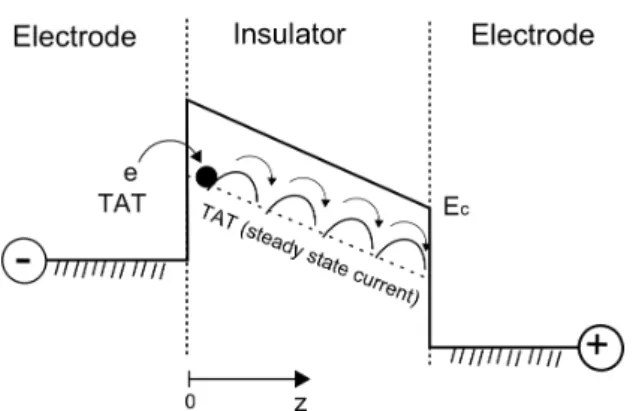
2.2.5 Theory of dielectric charging . . . 42
2.2.5.1 The model . . . 42
2.2.5.2 Dielectric polarization . . . 44
2.2.5.3 Charge injection mechanisms . . . 46
2.3 Focussed reliability concerns . . . 49
2.3.1 Dielectric charging in capacitive switches . . . 50
2.3.2 ESD/EOS specificities in MEMS . . . 51
2.3.2.1 ESD Testing standards . . . 52
2.3.2.2 Human Body Model (HBM) . . . 53
2.3.2.3 Transmission Line Pulsing (TLP) . . . 54
2.3.3 Operational power handling considerations . . . 54
2.3.4 Radiation effects . . . 56
2.3.4.1 Space radiation environment. . . 57
2.3.4.2 Radiation effect on materials . . . 58
2.3.4.3 RF-MEMS switches sensitivity to radiations . . . . 59
3 Experimentations: methodology, equipment and results 63 3.1 Hold-down charging studies on AlN devices and comparison . . . . 64
3.1.1 DUT . . . 64
3.1.2 Testing methodology and equipment . . . 65
3.1.2.1 The in-house RF-MEMS characterisation set-up . . 65
3.1.2.2 Microwave measurements . . . 66
3.1.2.3 Extraction of capacitance values from S-parameters 67 3.1.2.4 Switching times . . . 69
3.1.2.6 Hold-down charging . . . 70
3.1.3 Results and discussion . . . 71
3.2 ESD investigations in RF MEMS capacitive switches . . . 78
3.2.1 DUT . . . 78
3.2.2 Testing methodology and equipment . . . 79
3.2.2.1 TLP . . . 79
3.2.2.2 HBM . . . 80
3.2.2.3 Capacitance-based charging monitoring without pull-down of the switch . . . 81
3.2.2.4 Charging mechanisms hypothesis . . . 83
3.2.3 Results and discussion . . . 84
3.2.3.1 Breakdown phenomena in RF MEMS. . . 84
3.2.3.2 Charging studies . . . 89
3.2.3.3 Inhomogeneous dielectric charging . . . 92
3.2.3.4 Pulse induced accelerated stress test analyses . . . 95
3.3 RF power handling characterizations . . . 103
3.3.1 DUT . . . 103
3.3.2 Power handling setup . . . 104
3.3.3 Results. . . 104
3.4 Radiation effects in capacitive switches . . . 106
3.4.1 Experiment . . . 106
3.4.2 Results and discussion . . . 107
3.4.2.1 Radiation introduced vacancies . . . 107
3.4.2.2 Effect in MIM capacitors. . . 108
3.4.2.3 Effect in MEMS switches . . . 109
Conclusion 111 Outlook 113 List of Papers 127 Appendices 131 A Designs and Simulations 133 A.1 MEMS designs for RF applications . . . 133
A.1.1 Electro-Mechanical considerations . . . 134
A.1.2 Electro-Magnetic analysis . . . 135
A.1.3 Technology process . . . 136
A.1.4 Displacement characterizations . . . 137
A.2 MEMS protecting RF-MEMS . . . 139
1 The first integrated circuit.. . . 1
2 Vacuum tubes. . . 1
1.1 Xenon atoms on a nickel surface . . . 5
1.2 The first MEMS: a gold resonating MOS gate structure . . . 6
1.3 Fully integrated MEMS oscillators on CMOS . . . 6
1.4 Bulk micromachining . . . 8
1.5 Surface micromachining . . . 9
1.6 PIN diode and GaAs FET switch I-V graphs. . . 13
1.7 Typical S parameters of RF MEMS switches . . . 14
1.8 A K-band Single Pole Double Throw Circuit . . . 17
1.9 A 60 GHz Phase shifter. . . 17
1.10 V-band Tunable Band Pass Filter . . . 18
1.11 W- to V-band tunable resonator . . . 19
1.12 Tunable matching network . . . 19
1.13 The RF MEMS switch hype curve. . . 20
1.14 Companies in production of RF-MEMS. . . 23
1.15 The RF MEMS switch total market. . . 24
2.1 The ‘bathtub curve’ for reliability development. . . 32
2.2 The failure driven qualification methodology. . . 33
2.3 Principle of operation of a capacitive RF MEMS switch . . . 34
2.4 A measured C(V) curve of a capacitive RF-MEMS switch with its applied voltage waveform in the inset.. . . 35
2.5 Measured S-parameters of a 35 GHz capacitive RF-MEMS switch in both up-state and down-state configuration. . . 40
2.6 Simplified charging model of a capacitive switch, by analogy to the parallel plate model. . . 42
2.7 Charging mechanisms in RF-MEMS capacitive switches . . . 44
2.8 Dipolar or orientational polarization illustration. . . 45
2.9 Space charge and interfacial polarization illustration. . . 46
2.10 Energy level diagram illustrating an inelastic trap assisted tunneling process. . . 47
2.11 Energy level diagram illustrating the Poole-Frenkel conduction mechanism. . . 48
2.12 Operating parameters vs. device’s operation time. . . 49 xix
2.14 Log-log plot of the dielectric charging dependence on the stress time. 50 2.15 A microscope image of a capacitive switch submitted to several
HBM pulses (no apparent failure is visible). . . 52
2.16 A microscope image of a breakdown caused by EOS in a capacitive switch. . . 52
2.17 Short circuit current of common ESD-stress models. . . 53
2.18 The equivalent circuit used to test the discharge sensitivity of a device based on human body model. . . 53
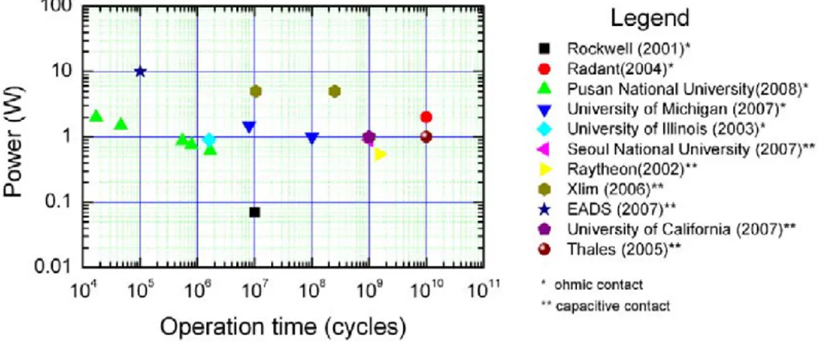
2.19 The equivalent electric circuit of the Transmission Line Pulsing set-up. 54 2.20 Hot-switching operation time and power handling capacity comparison of MEMS switches from worldwide publications. . . 56
2.21 The space radiation environment near the earth. . . 57
2.22 Space radiation environment inside and outside spacecraft. . . 57
3.1 Topology of the AlN-based capacitive RF-MEMS switches. . . 64
3.2 Diagram of test equipment setup for RF MEMS reliability monitoring. 65 3.3 Timing charts of microwave and switching measurements. . . 66
3.4 Measured S-parameters of the DUT. . . 67
3.5 The ABCD parameters of the equivalent 2-port circuit. . . 67
3.6 The extracted capacitance values. . . 68
3.7 The switching times. . . 69
3.8 Timing charts of control and detected signals. . . 69
3.9 Transmission parameter S21 vs. control voltage. . . 69
3.10 Timing charts of hold-down measurements. . . 70
3.11 Hold-down charging in AlN-based switches. . . 71
3.12 Empirical comparison of different insulating materials. . . 77
3.13 Tested devices. . . 78
3.14 S-parameters of (a) SW2 and (b) SW3 structures. . . 79
3.15 Block diagram of ESD set-ups including capacitance monitoring (a) TLP and (b) HBM. . . 79
3.16 Simple experimental apparatus employed here to measure mechanical variation of the movable membrane. . . 80
3.17 Principle of C(V) characteristic below the pull-down point. . . 81
3.18 Typical C(V) characteristic of the capacitive switch measured in the non-contact state voltage span. . . 82
3.19 The PIC test bench combine with a capacitance meter. . . 83
3.20 Charging mechanisms hypothesis in capacitive switch. . . 83
3.21 TLP Current-Voltage failure signature of SW1 switches.. . . 84
3.22 S21(V ) graph of SW1 affected by soft failures. . . 84
3.23 Microscope picture of a partially damaged switch. . . 85
3.24 Microscope picture of a completely destroyed switch. . . 85
3.25 Breakdown voltage in air at 1 atm versus gap. . . 86
DC voltage of 420V at the CPW access. . . 88
3.29 Current waveform responses in function of HBM failure signature. . 88
3.30 Optical checking (a) after the total stress is applied, (b) a zoom of the dielectric area after removing the bridge. . . 89
3.31 The shift of Vcapamin as a function of positive TLP pulses, for MF-SiN and LF-MF-SiN structures. . . 90
3.32 The shift of Vcapamin as a function of the magnitude of one positive HBM pulse. . . 90
3.33 Capacitance over time of devices submitted to one positive HBM pulse of 50V . . . 91
3.34 Non-contact C(V) curve for device which has been stressed at 50V for short pulse of10ms. . . 93
3.35 Surface potential distribution of a stressed device. . . 93
3.36 The shift of Vcapamin as a function of number of cycles. . . 96
3.37 The shift of Vcapamin as a function of the down-state duration tdown,s. 96 3.38 The shift of Vcapamin as a function of HBM stress electric field. . . . 97
3.39 The shift of Vcapaminas a function number of HBM pulses at different electric-fields. . . 97
3.40 The shift of Vcapamin as a function of the down-state time.. . . 98
3.41 Comparison between ∆Vc(Nc) and ∆Vs(Es). . . 98
3.42 The slopes as a function of the temperature. . . 99
3.43 The shift of Vcapamin as a function of stress voltage from 25◦C to 55◦C.. . . 99
3.44 Arrhenius model fit. . . 100
3.45 Capacitance transient response measured after the applied stresses during 1 hour. . . 100
3.46 Devices for power applications. . . 103
3.47 Measurement setup for high power testing at 10GHz. . . 104
3.48 Distribution of Si and N vacancy introduction rates (V) for a MIM capacitor. . . 107
3.49 TSDC spectra and stored charge of MIM capacitor obtained before and after each successive irradiation experiment. . . 107
3.50 Arrhenius plots of TSDC currents obtained before and after each successive irradiation experiment for (a) −20V and (b) +20V . . . . 108
3.51 Dependence of stored charge on radiation fluence for (◦) positive and (•) negative bias on top electrode. . . 109
3.52 Dependence of (◦) change capacitance at zero bias and (•) bias for capacitance minimum vs. radiation fluence.. . . 109
A.1 Different topologies of SPST switches. . . 133
A.2 Measured and simulated C(V) characteristics. . . 135
A.3 Measured and simulated S parameters characteristics. . . 135
A.8 Profilometer image and cross sections of BDG1 with the protection
structure. . . 140
B.1 Electrical schematic of the AST circuit for MEMS. . . 141
B.2 The AST-MEMS circuit. . . 142
4.3 Le marché total du commutateur MEMS RF [45]. . . 149
4.4 Principle de fonctionnement d’un switch MEMS RF capacitif (a) à
l’état haut (non actionné) et (b) à l’état bas (actionné). . . 151
4.5 Courbe C(V) complète du µ-commutateur MEMS RF capacitif. . . 152
4.6 Caractéristiques typiques du chargement du diélectrique et de la
défaillance.. . . 152
4.7 Modèle de chargement simplifié du µ-commutateur capacitf. . . 153
4.8 Chronogramme des signaux de commande et de la réponse du
µ − commutateur. . . 156
4.9 Comparaison empirique de différents matériaux diélectriques. . . 158
4.10 Courbes courant-tension TLP comme signature de défaillance. . . . 159
4.11 Une courbe typique de S21(V ) dans le cas d’un commutateur affecté
par des défaillances mineures. . . 159
4.12 Observations au microscope (a) après une série de décharge, (b) un
agrandissement du diélectrique après avoir enlevé la membrane. . . 160
4.13 La dérive de Vcapamin en fonction d’impulsions positives TLP, pour
les structures MF-SiN et LF-SiN. . . 161
4.14 La dérive de Vcapamin en fonction d’une impulsion positive HBM
pour des valeurs de tension allant de 30 à 100V, pour les structures
MF-SiN et LF-SiN. . . 162
4.15 La dérive de Vcapamin en fonction du nombre de cycles (avec
l’equivalence de la densité de charge en surface). . . 163
4.16 La dérive de Vcapamin en fonction du temps d’actionnement tdown,s. . 163
4.17 La dérive de Vcapamin en fonction du champ électrique du stress HBM.164
4.18 La dérive de Vcapamin en fonction du nombre d’impulsions HBM
pour différents champs électriques. . . 164
4.19 La dérive de Vcapamin en fonction du temps d’actionnement. . . 164
4.20 Comparaison entre ∆Vc(Nc) et ∆Vs(Es). . . 164
4.21 La dérive de Vcapamin en fonction du champ électrique à des
températures de 25◦C à 55◦C. . . . 165
1.1 Overview of functional materials used in MEMS . . . 7
1.2 MEMS structures and applications . . . 10
1.3 RF-MEMS devices, circuits and applications . . . 11
1.4 Main RF-MEMS switch designs . . . 12
1.5 Performance comparison of switches based on RF-MEMS, FET and
PIN diodes . . . 15
1.6 Main application fields of RF-MEMS switches . . . 16
1.7 Potential application fields of RF MEMS switches.. . . 22
1.8 Total volume needs of RF MEMS switches 2006 - 2011. . . 24
1.9 Fabrication technologies overview. . . 25
1.10aReliability summary of RF MEMS metal-contact switches. . . 28
1.10bReliability summary of RF MEMS capacitive switches and
switched-capacitors.. . . 29
2.1 Total dose levels for Earth orbits. . . 58
2.2 Overview of radiation effects on materials. . . 59
2.3 Overview of radiation effects on RF MEMS switches. . . 61
3.1 An overview of dielectric materials used in capacitive RF-MEMS. . 102
3.2 Comparative summary of RF MEMS power switch performance. . . 105
A.1 Physical dimensions of SPST switches shown in Fig.A.1. . . 134
4.2 Tableau comparatif de performance RF entre commutateurs
MEMS-RF, FET et diodes PIN [4, 5, 8, 24, 39]. . . 147
4.3 Les principaux champs d’application des micro-commutateurs
MEMS RF. . . 148
AF Acceleration Factors
ATE Automatic Test Equipment
BAW Bulk Acoutic Wave
CMOS Complementary Metal-Oxide- Semiconductor
CPW CoPlanar Waveguide
DARPA Defense Advanced Research Projects Agency
DBR Dual Behavior Resonator
DLP Digital Light Processing
DMD Digital Micro-mirror Device
DMTL Distributed MEMS Transmission Line
DRIE Deep Reactive Ion Etching
EOS Electrical Overstress
ESD ElectroStatic Discharge
FA Faluire Analysis
FBAR Film Bulk Acoustic-Wave Resonator
FET Field Effect Transistor (switch)
FMEA Failure Modes and Effects Analysis
GaAs Gallium Arsenide
HARMT High Aspect Ratio Microstructure Technology
HBM Human Body Model
IC Integrated Circuit
IL Insertion Loss
LIGA Roentgen-LIthography Galvanik Abformung
LTCC Low Temperature Cofired Ceramic
MMIC Monolithic Microwave Integrated Circuits
MOS Metal Oxide Semiconductor
MPW Multi Project Wafer
MST Micro Systems Technology
MTTF Mean Time To Failure
PA Power Amplifier
PF Poole-Frenkel
PIN Positive Intrinsic Negative (diode)
RF-MEMS Radio Frequency- Micro Electro Mechanical Systems
RIE Reactive Ion Etching
SCREAM Single Crystal Reactive Etch And Metal
SMR Solide Mounted Resonator
SOI Silicon On Insulator (substrate)
SoS Silicon on Sapphire
TAT Trapped Assisted Tunneling
TBPF Tunable BandPass Filter
TLP Transmission Line Pulsing
TSDC Thermally Stimulated Depolarization Current
TTF Time To Failure
ULSI Ultra Large Scale Integration
WLAN Wireless Local Area Network
A Capacitance area µm2
b Damping coefficient
C Capacitance value pF
Cdown Down-state capacitance value pF
Cmeas Measured down-state capacitance value pF
Cth Theoretical down-state capacitance value pF
Cup Up-state capacitance value pF
C0 The minimum of capacitance pF
d Distance between electrodes µm
Ea Activation energy eV
Emech The Young’s modulus N/mm2
Ee Distance-dependent electrostatic energy accumulated by the capacitor N · m
Er Restoring energy of the membrane N · m
Eef f Effective electric field intensity V /m
f0 Series resonant frequency Hz
F Radiation fluence m−2
Fe Electrostatic force N
Fc Sum of attractive and repulsive nuclear contact forces N
J Current density A.m−2
JP F Poole-Frenkel current density A.m−2
JS Schottky current density A.m−2
JT AT Trap Assisted Tunneling current density A.m−2
k Spring or force constant N/m
B Boltzmann’s constant
K Temperature acceleration factor
K0 Constant of the Arrhenius model
K1 Amplitude coefficient of the Arrhenius model
m Mass of the beam g
P Polarization q/Area
PP Total polarization q/Area
PD Dipolar polarization q/Area
PSC−i Intrinsic space charge polarization q/Area
PSC−e Extrinsic space charge polarization q/Area
Q Amount of charge C
Rsw Ratio between down-state and up-state capacitance
RQ Rate of charging
S21 Transmission coefficient dB
tdown Time the switch remains in the down-state s
ts Switching time s
t50 Median time-to-failure (electromigration) s
V Voltage V
Vcapamin Voltage corresponding to the minimum of capacitance V
Vdown Pull-down voltage V
Vdown−eq Equivalent pull-down voltage (power handling calculation) V
Vof f Offset voltage corresponding to the mean value of Vshif t V
Vshif t Offset voltage due to charging V
Vup Release-up voltage V
Vup−eq Equivalent release-up voltage (power handling calculation) V
z Displacement µm
zd Insulator layer thickness nm
Z0 Characteristic impedance Ω
∆ω Bandwidth Hz
∆P (t) Time-dependent polarization q/Area
∆Vc Shift of threshold voltages due to cycling V
∆Vs Shift of threshold voltages due to pulse stress V
ν The Poisson’s ratio for the bridge material
ωm Mechanical resonant angular frequency rad · s−1
σmech Mechanical stress in the beam P a
σp Parasitic charge density C/m2
σΣ Total surface charge density C/m2
Introduction
General introduction
In our information age, the micro- nano- world belongs to everyday life. The
beginning starts with, the first integrated circuit (Fig.1) successfully demonstrated
by Jack Kilby in 1958, which has revolutionized the world of electronics. Since
then down-scaling has increased in scope from vacuum tube technology (Fig.2) to
Ultra-Large Scale Integration (ULSI). Today we are able to integrate more than one hundred-thousand components on a single square centimeter chip.
Figure 1: The first integrated circuit. Figure 2: Vacuum tubes technology.
Microelectronic technology started with a few spots and wires on a chip of semiconductor, and has already grew into computers on chips. The significant successes of microelectronics is based on its ability for integration, miniaturization,
multifunctionality and high volume production. In this microworld conquest
Microelectromechanical systems (MEMS) appears to be a very good conqueror. They are very tiny systems that integrate functionalities from different physical
domains into one device. It is an extreme interdisciplinary field that
combines design, engineering and manufacturing expertise from diverse technical areas including integrated-circuit (IC), fabrication technology, materials science,
mechanical, electrical, chemistry and chemical engineering, as well as fluidics and optics.
Objectives of this thesis
In the pass years, communications were exclusively dedicated to military
and governmental uses. Nowadays the electromagnetic spectrum available for
telecommunication is quite broadband and civilian use constitutes a huge and important market. In order to adapt the evolution in the allocated frequencies, radical change in terms of flexibility and efficiency in architectures and systems
is required. It is than obvious that general communication systems will need
tunable and switching components that must be smaller, more secure, perform more functionalities and at the same time consume less power and have a very low noise behaviour.
“The RF chip has to work properly anywhere, anytime and has to be as cheap as possible” Robert Plana [1]
One very interesting and promising candidate, coming from the concept of micro-electro-mechanics is the Wireless MEMS, more famously called as RF-MEMS switch. Those devices have been demonstrated to gather performances such as; low insertion loss and high isolation, high linearity, high power handling and high Q factor, and low power consumption with respect to other microwave
switching technologies [2–5]. Mass production techniques from already existing
semiconductor industry can be used, which allows mass production and reduces unit prices.
However their restricted widespread integration is mainly due to the limited reliability data (i.e. operation time of RF-MEMS devices should be greater than 10 years). As a result, the reliability of RF-MEMS is still attracting many research interests. In order to be integrated into mainstream RF applications, they must demonstrate their reliability. One of the main challenges in this field is to identify and understand the failure modes so that accelerated stress tests can be developed. In this frame, this thesis focuses on the topic of reliability of RF-MEMS switches through:
• Charging,
• Electrostatic discharge, • Power handling,
• Radiation.
Obviously, from infinitely large to infinitesimally small, reliability aspects considered in this work require rather disparate disciplines and paradigms (e.g. material science, fabrication processing, mechanical engineering, physics, design and modeling engineering, simulations etc...). Therefore discussions with all the necessary experts was useful, appreciable and it has contributed to the writing of this manuscript.
Structure of this thesis
This manuscript deals with the reliability field of RF-MEMS. It is a interdisciplinary field involving the areas of integrated circuit fabrication
technology, mechanical and materials science, engineering of microscopic
mechanisms, and RF and microwave electronics engineering. Therefore the
document starts with an overview of the motivation and the activities in the field, from the micro- nano- world vision to the expected market forecast and the
present status and trend (Chapter1). The second part of this document integrates
fundamentals physics related to the focussed reliability research topics, in order to
provide references for further study of the related topics (Chapter2). The effect of
packaging on reliability is not discussed in this thesis. Furthermore, the scientific work of this thesis is based on, experimental results validating hypotheses on the failure behaviour and the failure mechanisms of the structures. Because standard reliability testing is not possible until a common set of reliability requirements
is developed (Chapter 3). Finally the manuscript ends with common conclusions
and gives a brief outlook over the possible continuation of the work described in this thesis.
Richard P. Feynman 1918-1988, American physicist in “There is Plenty of Room at the Bottom”
Chapter 1
Background
1.1
The micro- nano- world
Almost 50 years ago a american scientist named Richard P. Feynman predicted the future, the future of nanotechnology. It was 1959, only 2 years after the first satellite Sputnik 1 was lunched and 2 years earlier the first man Yuri Gagarin space walked. In that time, nobody had really seen an atom with a microscope.
His talk “There is Plenty of Room at the Bottom” [6] given on December 29th 1959
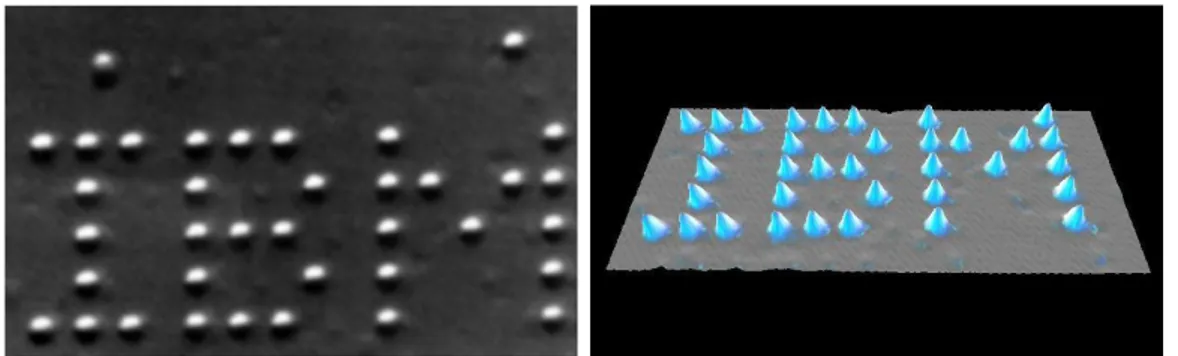
at the annual meeting of the American Physical Society at the California Institute of Technology, will become a roadmap for nanotechnology. Feynman predicted how technology may make things smaller and smaller. Forty years after, in 1989 Don Eigler and his research group moved individual atoms. They used 35 atoms to
spell out IBM (Fig. 1.1). Today we are using nanotechnology and making things
smaller and smaller. The world of objects that are smaller than a wavelength of visible light “the micro- nano- world” belongs to everyday life.
Figure 1.1: Xenon atoms on a nickel surface
1.2
MicroElectroMechanical Systems
1.2.1
Definition
The world of MEMS is so small that it is not imperceptible to the human eye. A world where volume effects such as gravity and inertia are no longer important, but atomic forces and surface science such as electrostatics and wetting dominate. “MEMS” also referred to as micromachines in Japan or Micro Systems Technology (MST) in Europe, are very tiny systems (its size is comparable than a grain of pollen) that integrated microstructures combining electrical and mechanical properties. These systems have the ability to sense, control and actuate in order to interact with physical, chemical surroundings such as motion, sound, light, radio waves, gases, liquids, thermic radiation etc. A whole new class of micro-products performing tasks on the microscale and generating effects on the macroscale has emerged. MEMS is one of the most exciting and huge evolution in microelectronics, a “smart matter” in a small world with big opportunities.
In 1967, less than 10 years after the invention of the IC (Fig.1), H. C.
Nathanson used microelectronic fabrication processes to make the first MEMS
device [7], which was a gold resonating MOS gate structure (Fig.1.2). Since this
demonstration, the progress in this field never stops. Nowadays, MEMS technology has reached the maturity as silicon resonating market threatens the quartz crystal one. In fact, Discera, SiTime and Silicon Clocks are already manufacturing silicon MEMS oscillators , and Toyocom (Seiko Epson) produces micromachined quartz MEMS oscillators. This is a nice representation of MEMS on CMOS integration.
Drain Diffusion Drain bias voltage
Input signal (Vac) Polarization voltage (Vp) Channel Source diffusion Oxide Silicon substrate
Figure 1.2: The first MEMS: a gold resonating MOS gate structure
Figure 1.3: Fully integrated MEMS oscillators on CMOS (Courtesy of
Substrates Ceramics Metals
Silicon/SOI Silicon dioxide (SiO2) Gold (Au)
Quartz Silicon nitride (Si3N4) Aluminium (Al)
Glass Alumina (Al2O3) Nickel (N i)
Gallium arsenide Aluminium nitride (AlN ) Chromium (Cr)
Polymide flexible Titanium dioxide (T iO2) Titanium (T i)
Tantalum pentoxide (T a2O5) Tungsten (W )
Hafnium oxide (Hf O2) Platinum (P t)
Barium strontium titanate (BST ) Silver (Ag)
Zinc oxide (ZnO) Tantalum silicide (T aSi2)
Lead zirconate titanate (P ZT ) Polysilicon
Table 1.1: Overview of functional materials used in MEMS
1.2.2
Materials and fabrication
In a sense, MEMS technology is an “turn old into new” technology because significant parts of the technology has been adopted from IC know-how (the use of silicon wafer, thin films of materials, photolithography technique etc.). Since there is a wide variety of materials having physical properties suitable for MEMS devices, this section does not attempt to present a comprehensive review of all of them but a short introduction to the basic fundamentals of materials and technologies is absolutely necessary to design, model, fabricate and characterize MEMS.
1.2.2.1 Materials
Depending on the function and the operating environment of MEMS devices, the
selection criteria of the materials will change (Section 1.6 in [8], Chapter 3 in
[9]). For instance, if we consider MEMS mechanical resonators and switches, we
want materials that have high quality factor and low electrical resistivity to reduce
insertion loses and chargingless material as insulator. Table1.1 gives an overview
of functional materials used in MEMS. These three main classes of materials are used to structure most of the MEMS devices using basic fabrication techniques such as deposition, patterning (by photolithography) and etching.
1.2.2.2 Bulk micromachining
In 1979, K. E. Petersen reported “Micromechanical Membrane Switches on Silicon”
categories of MEMS technologies is bulk micromachining. As it is shown in Fig.1.4, it consists in using etching techniques (anisotropic or isotropic wet etching and deep-reactive ion etching (D-RIE), sputter and vapour phase etching) to selectively etch away unwanted parts and create suspended structures. These techniques allow the fabrication of a multitude of micromachined sensors, actuators, and mechanical
structures ([11],Chapter 3 in [12],Section 1.3.1 in [8], Section 1.2.1 in [9]).
(a) (b)
Figure 1.4: Bulk micromachining (a) anisotropic wet etching (b) deep reactive ion etching (Courtesy of DARPA)
1.2.2.3 Surface micromachining
The recent emergence of higher resolution results in adopting surface
micromachining approaches. Contrary to bulk micromachining, here devices
are fabricated by structuring layer-by-layer (Chapter 3 in [12], Section 1.3.2 in
[8], Section 1.2.2 in [9]). The Fig.1.5 depicts typical steps used in the surface
micromachining process. The sequence is often composed by; depositing thin
films on a wafer, patterning by photolithography and then etching the patterns into the films. The use of sacrificial and structural materials makes mechanical elements to move and fulfil its function.
E. Garcia and J. Sniegowshi from Sandia National Lab. have shown a whole
1.2.2.4 High aspect ratio processes The depth of etching can be increase using high aspect ratio microstructure technology (HARMT) such as LIGA, DRIE and SCREAM, to name a few. LIGA is a German acronym of Roentgen-LIthography
Galvanik Abformung, describing the
process sequence; X-ray lithography,
electrodeposition and moulding [14, 15].
SCREAM process stands for Single Crystal silicon Reactive Etch and Metal and use submicron optical lithography to defines MEM devices with a single mask
[16, 17]. In HAR silicon micromachining
the thickness can be from 10 to 100µm whereas it is only around 2µm in basic
micromachining processes. HARMT
gives the possibility to fabricate a wider array of mechanical elements.
Figure 1.5: Surface micromachining [18]
1.2.2.5 Wafer bonding
Originated from the development of silicon-on-insulator (SOI) wafers, bonding techniques (anodic bonding,intermediate-layer assisted bonding and direct bonding) can combine silicon and bulk micromachining for building complex 3D microstructures in a monolithic format. The principle deals with the creation of atomic bonds between two wafers either directly or through a thin film (Section
1.3.4 in [19] and section 1.3.3 in [8]). As a result, further advanced MEMS
structures in the field of pressure sensors, accelerometers and resonant structures can be developed and assembled.
1.2.3
Products
It is remarkable how using relatively easy processes, we can create unlimited
structures, just “our ideas limited”. MEMS keep creating new capabilities,
Sensor/Actuator/Structure Functions/Physical surroundings Categories Field of application (commercial/military) Pressure sensors Mechanical deformation Thermal expansion Inertial Vibration Mechanical MEMS Biomedical Automotive Robotics Consumer electronics Multimedia Telecommunication Mobile phone Watch industry Earthquake Detection Gas Shutoff
Shock and Tilt Sensing
Biochemical warfare
detection
Inertial systems for guidance and navigation
Equipment for Soldiers Aeronautics Aerospace Accelerometers Gyroscopes Comb drivers Piezo-resistors
Micro resonant strain gage Temperature sensors Blood pressure sensors
Lab on chip Drug delivery Neural probes Breating rate Heart rate Sense organs Bio- Fluidic- Chemical-MEMS Biocapsules Bioneedles Micro-pumps Micro-valves Micro-resevoirs Micro-actuators Bio-potential electrodes Chemosensor
Interferometric modulator display
Optical modulation Digital Light Processing Light deflection and control
MOEMS MEMS Display MEMS Polychromator
Micromirrors Digital MEMS shutter
Inkjet printers pins nozzles Multimedia
MEMS
Microphones Acousticwave
MEMS Actuator array
Data storage MEMS Memory
Thermal MEMS Micro- fuel cells/reactors
Power MEMS Micro- heat engines/coolers
RF switches/varactors/oscilators
Microwave RF MEMS
single and multi-throw switches Phase shifters
Tunable filters/matching networks Switch matrices
Table 1.2: MEMS structures and applications
summarize a part of it. Most of them are fully commercialized and MEMS success stories have been achieved by pressure sensors,accelerometers, inkjet print heads and DLP mirror array. One single look at the call of paper of IEEE-MEMS 2010 conference is enough to realize that the area of activity in the development and application of MEMS is extremly wide.
1.3
RF-MEMS technology
The first radio frequency - microelectromechanical systems (RF-MEMS) were
developed under one of DARPA programs. It was in 1991, L. E. Larson [20]
presented an MEMS switch and an varactor, specifically designed up to 45GHz. In spite of the immaturity of the RF-MEMS technology at that time, two cutting-edge designs have been demonstrated; one was an ohmic switch coming from
Rockwell Science Center [21] and the second one was capacitive contact switch from
Texas Instruments [22]. Since then RF-MEMS start to evolute and technologically
progress. The fact that RF-MEMS technology suits well to the strong demand for flexibility, complexity, lightweight and low power consumption of advanced
Performance of RF MEMS switches is truly spectacular when compared to PIN diode or FET switches
Gabriel M. Rebeiz [4]
wired and wireless systems, triggers many interest from research institutes and
universities [1–4, 23–26]. From 1995 (considered as the RF-MEMS technology
trigger point) up to now, a huge number of publications presenting new RF-MEMS concepts follow one after the other but only by the end of the 1990s the research
included device reliability issues [27–29]. In fact, the scope of the reliability topic in
RF-MEMS goes together with the apparition of MEMS with contacting/touching parts (metal to metal, metal to insulator, metal to substrate or insulator to substrate). From then on new physics of failure and failure mechanisms appears
out of this energy transfer [30]. RF-MEMS technology is composed fundamentally
by building blocks listed in Table 1.3. Finally performance enhancements and
manufacturing cost reduction are evident characteristics of this technology and it is finding its way into next generation timing, wired and wireless applications.
RF-MEMS building blocks (a-b,c) RF-MEMS circuits RF-MEMS applications
High-Q µ-mechanical resonators and oscillators (1-125MHz,2.5GHz)
MEMS high-Q inductors (1.1-8GHz) BAW resonators** (0.5-11GHz)
Tunable capacitros(0.1-100GHz,220GHz) Cavity resonators(40-100GHz,15GHz) MEMS switches(0.1-100GHz,220GHz) Other microwave and milimeter-wave components Single and multi-throw circuits Phase shifters Tunable filters Tunable matching networks Timing oscillators Switch matrices Programmable attenuators Reconfigurable antennas Mobile handsets
Consumer electronics and Information Technology
Wireless network systems (WLAN/WPAN) Base stations
Microwave communications RF test and ATE equipment Automotive radar and antennas Satellite transponders
Phased arrays* Tactical radio*
* military
** include FBAR and SMR devices
a−boperative frequency range
cupper or lower limit (need more development efforts)
Topologies Ideal Equivalent circuits
Series ohmic in-line configuration* Series ohmic
Series capacitive
Shunt capacitive
Shunt capacitive configuration*
Shunt ohmic
* topologies that works better
Table 1.4: Main RF-MEMS switch designs
1.3.1
RF-MEMS switches
1.3.1.1 The designs
RF-MEMS switches are basically used to make a short circuit or an open circuit in the RF transmission line. They can be designed to work at electrical operating
frequency from 0.1 up to > 200GHz [31]. Their mechanical displacement can
be generated from field forces (electrostatic and magnetic) or molecular forces (piezoelectric, electro-thermal, bi-metallic) and ranged typically from 0.1 to 3µm.
The two main topologies are catalogued in Table 1.4 – serial and shunt switches,
with their ideal and “realistic” equivalent models. Based on these two categories, a huge variety of designs has been demonstrated by optimizing the mechanical
structure (cantilever, fixed-fixed beam, two-pull down electrodes, lateral anchors,
U-shape membrane ...) as well as the aforementioned actuation mechanisms
in order to achieve fast switching, low actuation voltage operation (also called control, command or pull-in voltage) or high power handling.
(a) (b)
Figure 1.6: Typical I-V graphs of PIN diode and GaAs FET switch, with their microwave equivalent circuit (a) PIN diode (b) GaAs FET device (in the low impedance
and high impedance states).
Note: Microelectronic RF switching technologies
I PIN Diode is a diode with a intrinsic semiconductor region inserted in between two
p-type and n-type doped regions. As shown in Figure1.6(a), when forward biased (on-state)
the device exhibits a very low resistive impedance and when reverse biased (off-state) it gives a high-frequency resistance in parallel with a low capacitance. PIN diodes are useful as RF switches (phase shifters), attenuators, and photodetectors.
I FET Switch is a semiconductor device considered as a type of transistor. Its specific characteristics is the use of an electric field to control the shape and hence the conductivity
of a channel of one type of charge carrier in a semiconductor material. Figure1.6(b) shows
that to work like a switch, the FET is DC biased at zero drain-source voltage (Vds = 0V ),
and the gate is biased either zero bias in its low impedance state (on-state) or pinch-off in its high impedance state (off-state) i.e. when a negative voltage with respect to the channel is applied. FET switches are often used in digital electronics (Boolean operations), power controls, audio amplifiers and RF switching blocks.
1.3.1.2 RF performances
Comparing microelectronic RF switching technologies, RF MEMS switches offer a substantially higher performance than its electronic counterparts; PIN diode and FET switches. The parameters taken for the comparison are : power consumption, losses, isolation, linearity, manufacturing and final product cost, speed, power handling and control voltage. The comparison survey of the properties is listed
out in Table 1.5.
leading to a very low power dissipation [4]. For instance, in a phased array antenna, to perform a 2D scanning, there’s over 4000 phase shifters, where each 4 bits phase shifter integrates around 14 elements. If each diode consumes [email protected] DC current, then the 2D scanning will needs 178W instead of only 0.01W if it is done using RF-MEMS switches.
⊕ RF-MEMS switches are made up of suspended membrane, therefore in series switches the air gaps provide very low off-state capacitance (2-4 fF) resulting in
very high isolation at 0.1 - 40 GHz [4]. By the same way, the insertion loss in
RF-MEMS switches is less than 0.1 dB up to > 40 GHz. Typical scattering parameters
of series ohmic and shunt capacitive configurations is shown in Fig.1.7.
(a) (b)
Figure 1.7: Typical S parameters of RF MEMS switches (a) series ohmic and (b) shunt capacitive
⊕ In terms of linearity, RF-MEMS switches does not suffer from nonlinear
I-V relationship compared to semiconductor switches. It results in very low
intermodulation products.
Since RF-MEMS technology processes are done, using surface or bulk micromachining techniques, with low cost materials and less process steps (Section.
1.2.2), its manufacturing cost amounts to very low. Unfortunately, its final product
cost increase with the cost of packaging and the high-voltage drive chip.
⊕ Another very interesting parameter is its ability for integration. Thanks to its relatively easy fabrication processes, RF-MEMS switches can be manufactured with MMIC processes on any substrate material including silicon, GaAs, glass (Pyrex), alumina and also low-temperature cofired ceramic (LTCC).
The switching time of RF-MEMS switches usually ranges from 1 to > 20 µs, which is too long compared to its counterparts one (especially for
Parameter Unit RF-MEMS FET switch PIN diode
Size mm2 <0.1
∼ 1 0.1
Control voltage V 3 – 80 1 – 10 3 – 5
Control current µA <10 <10 3K – 10K
Current handling mA ∼ 200 ∼ 200 > 20 Power consumption mW ∼ 0.001 – 0.05 1 – 5 1 – 5 Power handling W <4 <10 <10 Insertion loss dB 0.1 up to 120 GHz 0.4 – 2 up to 10 GHz 0.3 – 1.0 up to 10 GHz Isolation dB > 30 up to 100 GHz 15 – 25 up to 10 GHz 20 – 35 up to 10 GHz Switching time ns >300 1 – 100 1 – 100 Bandwidth GHz 10 - 30*/ <100** n/a 0.02–2 Cutoff frequency THz 20 – 80 0.5 – 2 1 – 4 Third-order intercept point dBm > 60 40 – 60 30 – 45 Up-state capacitance fF 1 – 10 fF** 70 – 140 18 – 80 Series resistance Ω <1 4 – 6 2 – 4 Capacitance ratio – 40 – 500* – 10 Lifetime Cycles >a1013or >b107 > 109 > 109 Final cost $ 8 – 20 0.3 – 6 0.9 – 8 * shunt capacitive ** series ohmic acold switching bhot switching
Table 1.5: Performance comparison of switches based on RF-MEMS, FET and PIN diodes [4,5,8,24,39]and updates.
telecommunication and radar applications). However it is possible to create
sub-microsecond switching RF-MEMS devices [32,33] in compensation for high control
voltage.
In general, RF-MEMS switches can operate and handle in the range of 0.02– 0.8W in power. Fortunately several promising designs have been shown handling
up to 4 and 8W [34–38].
The fact that the actuation voltage of reliable electrostatic RF-MEMS switches is often very high, requires additionnal voltage up converter chip when integrated in portable systems.
Finally, the two main issues of RF-MEMS switches is the packaging and the
reliability. They need to be packaged in inert atmospheres (nitrogen, argon,
hydrogen, helium) and (quasi-)hermetic seals. Currently, packaging cost is still a part important of the final product and the package itself can affect the reliability of the device. The reliability of mature RF-MEMS devices can reach a few billion
cycles. However electronic systems require more than 10 years reliability and
long-term test has not yet been addressed. Reliability “in the large sense of the word ” and accelerated lifetime test in RF-MEMS will be the main concern of this manuscript.
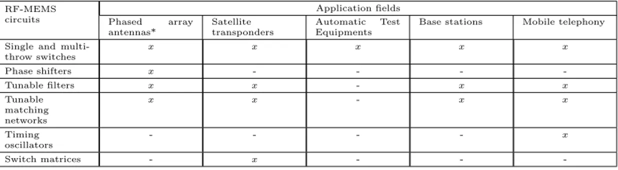
RF-MEMS circuits Application fields Phased array antennas* Satellite transponders Automatic Test Equipments
Base stations Mobile telephony
Single and multi-throw switches x x x x x Phase shifters x - - - -Tunable filters x x - x x Tunable matching networks x x - x x Timing oscillators - - - - x Switch matrices - x - - -xmight be implemented in
* military, aeronautic, automotive radars
Table 1.6: Main application fields of RF-MEMS switches
1.3.2
Applications of RF-MEMS switches
RF-MEMS technology is entering into the next generation timing and wireless
applications. This technology has opportunities in analogue and digital
applications, such as in satellite and fibre-optic communication systems, in cellular phones and other wireless equipment, in automatic test equipment, and for other diverse civilian and military uses. This concept enables superior reconfigurable functions, using in particular;
• Switching networks/Switch matrices/Switched filter banks for satellite and wireless communication systems.
• Phase shifters/Phased array antennas for satellite based radars, missile systems, long range radars and automotive radars.
• High-performance switches/Programmable attenuators for instrumentation systems.
Table 1.6 shows the possibilities of RF-MEMS circuits that may be implemented
into the system level. The very interesting performances of RF MEMS
switches (both metal-contact and capacitive) have triggered a thousand and one inventiveness of many designers to build cutting-edge switching circuits in the frequency range of 0.1 to >120 GHz. In terms of illustration, instead of presenting state of art components, this section shows examples of several RF-MEMS circuits designs from LAAS-CNRS.
A ctu ato r S w itc h C on tro l A ctu ato r S w itc h C on tro l RF1 RF2 RF3
Figure 1.8: A K-band Single Pole Double Throw Circuit (designed by V. Puyal )
1.3.2.1 Single Pole Double Throw
Single-pole N-throw (SPNT) switches are often used in N×N switching matrices and filter or amplifier selection. The basic one is the SPDT (single-pole
double-throw) routing switch. The one shown in Figure 1.8 is build with K-band shunt
switches. It consists of a tee with a RF-MEMS at each of the output(RF2 and
RF3). The switches are placed at a distance of a quarter guided wavelength from
the tee junction so that when one switch is actuated, the virtual RF short is assimilated as an open at the junction and the signal is routed away toward the other RF path. RF-MEMS based SPNT becomes very attractive over their solid state counterparts, mainly prompted by the power consumption and the linearity. They result in much smaller and lighter systems as well, which is for instance essential for satellite applications.
1.3.2.2 Phase shifter
Figure 1.9: A 60 GHz Loaded-line Phase shifter (designed by V. Puyal )
RF-MEMS based phase shifters exist in several configurations namely switched line , loaded-line, reflection and high-pass/low-pass. This example deals with a
1-bit V-band loaded-line (22.5 degree) phase shifter [40] (Figure 1.9). The two
circuit, while they have only a small effect on the amplitude of the signal. The amplitude perturbation can be minimized and equalized using a quarter-wavelength spacing between the reactive loads. In terms of phase versus frequency response, this kind of phase shifter is usually flatter than the switched line phase shifter, but less flat than the high-pass/low-pass phase shifter. Only one control signal is required for this loaded-line phase shifter, since the loads can be biased simultaneously. The implementation of phase shifter in phased array antennas allows the development of passive reflect array at X- to W-band frequencies. The cost is also another factor because reflect arrays are much less expensive than standard phased arrays.
1.3.2.3 Tunable filter
Tunable filters are key elements used in advanced transceiver architectures. Bandpass filter is used for its good selectivity and sensitivity and bandstop filter is used to eliminate undesired signals such as spurious responses or cross-talk interferences (in transceiver configuration). From design to characterisation,
both aforementioned tunable filters have been presented in [41]. It consists of
using CPW quarter wavelength stubs and MEMS switches : two cantilever shunt
switches. The example shown in Figure 1.10 is the TBPF topology. The stubs
have different geometrical lengths, which are translated into two zeros in the transmission coefficient and it results in a bandpass behaviour. Adding a MEMS switch at the end of the stubs will makes the filter tunable.
(a) (b)
Figure 1.10: V-band Tunable Band Pass Filter (a) fabricated device and (b) simulated transmission coefficient [41]
1.3.2.4 Tunable dual behaviour resonator
Another interesting tuning element is the dual behaviour resonator (DBR) because
it allows the control of two attenuated bands on either side of one bandpass [42].
In fact the DBR topology consists of two different open-ended stubs which bring a transmission zero on either side of a pass-band. MEMS switches can be used to change the length of the inter-stubs line in order to tune the center frequency
and keep a correct matching level. Figure 1.11 shows a DBR resonator which was
realized in thin film microstrip technology implemented in Si-BCB substrate.
Figure 1.11: W- to V-band tunable resonator [43]
1.3.2.5 Tunable matching network
Tunable matching network is interesting to be used in real-time adaptable RF front-ends, in order to maintain low loss and high linearity. Implementing RF-MEMS within such a system will minimize degradation to the overall amplifier
performance. The design shown in Figure 1.12 illustrate impedance tuner based
on the distributed MEMS transmission line (DMTL). The main idea is to maintain the matching performance over a broad bandwidth by changing the physical length of the transmission line.
Figure 1.13: The RF MEMS switch hype curve [44].
1.3.3
Industry and market roadmap
In this section, a survey has been carried out of several market studies from WTC,Yole Development,ARRRO (Applied Research Roadmaps for RF MEMS Opportunities), iSuppli Corporation and Mancef, in order to state today’s market of RF-MEMS switches and foresee the RF MEMS switch volume needs upto 2012. It will let us have a glance to the global economic and market background. MEMS components have emerged in the mid-1990s under a DARPA’s military
radar program [10]. RF-MEMS switches came into the spotlight only in the
early 2000s. With their remarkable RF performances, RF-MEMS components have created a lot of excitement, but their commercialization is eagerly-awaited.
Happily, if we look at the hype curve1 of RF MEMS (Figure 1.13), it shows that
RF MEMS switches will reach the “Plateau of productivity” soon, as the industry and technology are both maturing. The first commercial micromachined RF device was the FBAR duplexer from Agilent Technologies. It is a set of piezoelectric filters that separate incoming and outgoing signals in the frequency range of 800 MHz and 1900 MHz. But it may not be complex enough to be considered as a “true” MEMS. In the meantime, other RF MEMS products have become commercially available, including switches (Omron, Radant, XCOM Wireless, Wispry...), inductors and micro-mechanical resonators (Discera, SiTime, Silicon Clocks). In order to be consistent, all roadmap studies:
1. The hype curve was first proposed by Gartner, an analyst/research house based in U.S. as a way to place technologies in their particular stage of evolution
• considered the stand-alone device and not global systems that include MEMS devices,
• volumes and prices are for the lowest level packaged MEMS device,
• and consisted of in-depth interviews with around 100 key industry experts in the field of MEMS technology.
The market forecasts have been done by paying attention to (1.3.3.1) the potential
applications of RF MEMS switches, (1.3.3.2) major companies in production and
also (1.3.3.3) the total volume needs upto 2011.
1.3.3.1 Potential applications
RF MEMS switches are in development for a very wide spectrum of applications. For the market analysis it can be fragmented into six major application fields
(Table 1.7);
• Automated Test Equipment (ATE) for semiconductors is the first commercial
application for RF MEMS switches. Here the use of RF MEMS switch is to
replace conventional relays without changing the whole system and therefore the implementation of MEMS is quick and easy. While its integration into RF
instrumentation equipment is expected at the earliest in 2009, mostly due to power handling issues.
• Cell phone industry was very interested to use RF MEMS technology to develop T/R switch, multiband filters, filter banks, impedance matching networks, and so on. But reliability and packaging difficulties, represented by the
“trough of disillusionment” phase in Figure 1.13, created a lot of disappointment.
Nevertheless, NXP, RFMD and WiSpry still believe and develop impedance matching networks for the power amplifier (PA) or MEMS-based reconfigurable antenna module, which offer the best prospects for RF MEMS switches in this market.
• Automotive applications such as RF MEMS based long range radar or phase shifter technology for phased array, have no envisioned opportunities for RF MEMS in the 2006-2012 time frame. The market is dominated by SiGe technology (3rd generation of 77 GHz ACC systems / Precrash systems).
• Satellite applications tend to evolute towards higher frequencies and increase
the integration with greater functionality. Consequently, there’s is a need for
complex redundancy scheme, large microwave routing network and reconfigurable antennas. RF-MEMS switches fit well to the specific space application needs.
![Table 1.5: Performance comparison of switches based on RF-MEMS, FET and PIN diodes [ 4 , 5 , 8 , 24 , 39 ] and updates.](https://thumb-eu.123doks.com/thumbv2/123doknet/2140161.8834/47.893.165.785.121.476/table-performance-comparison-switches-based-mems-diodes-updates.webp)