HAL Id: lirmm-00968621
https://hal-lirmm.ccsd.cnrs.fr/lirmm-00968621
Submitted on 5 Oct 2016
HAL is a multi-disciplinary open access
archive for the deposit and dissemination of sci-entific research documents, whether they are pub-lished or not. The documents may come from teaching and research institutions in France or abroad, or from public or private research centers.
L’archive ouverte pluridisciplinaire HAL, est destinée au dépôt et à la diffusion de documents scientifiques de niveau recherche, publiés ou non, émanant des établissements d’enseignement et de recherche français ou étrangers, des laboratoires publics ou privés.
A single built-in sensor to check pull-up and pull-down
CMOS networks against transient faults
Rodrigo Possamai Bastos, Frank Sill Torres, Jean-Max Dutertre, Marie-Lise
Flottes, Giorgio Di Natale, Bruno Rouzeyre
To cite this version:
Rodrigo Possamai Bastos, Frank Sill Torres, Jean-Max Dutertre, Marie-Lise Flottes, Giorgio Di Natale, et al.. A single built-in sensor to check pull-up and pull-down CMOS networks against transient faults. PATMOS: Power and Timing Modeling, Optimization and Simulation, Sep 2013, Karlsruhe, Germany. pp.157-163, �10.1109/PATMOS.2013.6662169�. �lirmm-00968621�
A Single Built-in Sensor to Check Pull-up and
Pull-down CMOS Networks against Transient Faults
R. Possamai Bastos1, F. Sill Torres2, J.-M. Dutertre3, M.-L. Flottes4, G. Di Natale4, B. Rouzeyre4
1TIMA Laboratory (Grenoble INP, UJF, CNRS), Grenoble, France ([email protected]) 2UFMG (Dept. of Electronic Engineering), Belo Horizonte, Brazil ([email protected]) 3Centre Microélectronique de Provence - Georges Charpak, Gardanne, France ([email protected])
4LIRMM (Université Montpellier II / CNRS UMR 5506), Montpellier, France ({flottes, dinatale, rouzeyre}@lirmm.fr) Abstract—This work presents a novel built-in current sensor for
detecting transient faults of short and long duration as well as multiple faults in combinational and sequential logic. The sensor is a single mechanism connected to PMOS and NMOS bulks of the monitored logic. With no performance penalty, very competitive results indicate overheads of only 26 % in power consumption and 23 % in area.
Keywords: Built-in current sensors, concurrent detection, fault tolerance, security, soft errors, transient faults
I. INTRODUCTION
Integrated systems based on ultra-deep submicron technologies require higher robustness to natural aging processes or radiation environmental sources [1]. These natural phenomena on integrated circuits can induce transient effects that provoke bit-flips of stored results during the system lifetime. Among the several strategies to detect transient faults caused by radiation or optical sources, Bulk Built-In Current Sensors (BBICS) offer a promising solution that is perfectly suitable for system design flows based on CMOS standard cells of commercial libraries. BBICS have the high detection efficiency of costly fault-tolerance schemes (e.g. duplication with comparison) with the low area and power overheads of less efficient mitigation techniques such as time redundancy approaches. Without impacting on system operating frequency, BBICS deal with transient faults of short and long duration as well as multiple faults. Furthermore, as they closely monitor the zones where the faults arise, an early detection is possible immediately after a fault occurrence, preventing induction and propagation of errors to other clock cycles or system blocks.
All today’s BBICS-based strategies [1][2][3][4] [5][6] use two different circuits that monitor independently PMOS and NMOS bulk currents from pull-up and pull-down CMOS networks. We present in section III and IV of this paper a new lower area
BBICS version compounded of a single circuit that is able to monitor both CMOS networks. Important preliminary related information regarding built-in current sensors is before discussed in section I.
II. BICSDETECTING TRANSIENT FAULTS
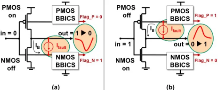
The use of Built-In Current Sensors (BICS) in the bulk for monitoring circuit allows the detection of a wide range of transient faults; such a smart idea was introduced for the first time in [1]. Fig. 1 (a) and (b) illustrate Bulk BICS (BBICS) identifying anomalous transient currents Ifault that flow through the junction
between a bulk and a reversely biased drain of a disturbed transistor (MOSFETs “off” in Fig. 1). BBICS indeed take advantage of two facts: (1) In fault-free scenarios (i.e. Ifault = 0) the bulk-to-drain
(or drain-to-bulk) current IB is negligible even if the
MOSFET is switching in function of new input stimuli; (2) During transient-fault scenarios, Ifault is
much higher than the leakage current flowing through the junction. The range of detectable transient faults is easily adjustable by calibrating the size of the transistors that constitute the BBICS. Hence, schemes based on BBICS can be designed to latch a flag of fault indication for abnormal currents within a defined range that represents a risk of resulting in soft errors.
Figure 1. The two classic cases of transient faults in a CMOS inverter perturbed by an anomalous current Ifault
III. NEW SINGLE BBICS
The classic BBICS-based strategy is using a pair of sensors (PMOS and NMOS) to monitor pull-up and pull-down networks – e.g. PMOS-BBICS 1 and NMOS-BBICS 1 in Fig. 2 (a). The capacity of each sensor for identifying transient faults is limited to a certain number of monitored transistors. Hence the strategy is also splitting the target system into blocks with the maximum possible number of transistors the sensor is able to monitor. Fig. 2 (a) illustrates an example of system (chains of inverters) divided into two blocks that are monitored by two pairs of BBICS. For the same example, our strategy is otherwise to use single sensors for up and pull-down networks as Fig. 2 (b) shows.
Figure 2. (a) The classic BBICS-based strategy with pairs of BBICS (NMOS and PMOS) monitoring blocks of a system; and (b) Our strategy with
the new single BBICS able to check both pull-up and pull-down networks A. Structure of Sensor
The structure of the new single BBICS presented in this paper takes the high fault-detecting capacity of the sensors proposed in [4] and illustrated in Fig. 3 (a). Moreover, it was optimized from a pair of sensors to a single sensor and, consequently, the area could be significantly reduced as we can see in Fig. 3 (b) compared with Fig. 3 (a) in terms of transistor counting. Low leakage power overheads are met by finding the optimal number of monitored transistors as discussed in section IV. In Fig. 3, Wmin represents
the minimum diffusion width of the transistors, Lmin
is the minimum channel length, and design factors
Xn, Yn, Xp, Yp, X and Y are used for calibrating the
sensor with a desired fault-detecting capacity.
Transistors 5, 6, 7, and 8 in Fig. 3 (b) constitute the latch used to memorize a flag (i.e. output Flag at
Vdd) in case of a transient fault within a defined
range of current that temporally perturbs the monitored pull-up or pull-down network. In addition, the latch transistors are responsible for amplifying the anomalous transient currents coming from node NMOS_Bulk or going to node
PMOS_Bulk of monitored blocks. Factors X and Y
allow increasing the gain of amplification and, thus, configuring the sensor with higher fault-detecting capacity. Transistors 11 and 12 are used to set the sensor in sleep-mode when the system is left on standby (i.e. signal Sleep_Mode at Vdd). It leads to
zero the offset on the bulk voltage of the monitored block, and so the sub-threshold leakage power consumption is significantly reduced.
B. Mode of Operation
In fault-free conditions and inactive sleep mode (i.e. Sleep_Mode at gnd), the proposed structure in Fig. 3 (b) has in theory NMOS_Bulk at gnd level and
PMOS_Bulk at Vdd. Signal Flag is at gnd; node1 at Vdd; and transistors 1, 3, 4, 10, 11, and 12 are in
off-state. Further, as transistors 2 and 9 are in on-state, they impose, in reality, on NMOS_Bulk and
PMOS_Bulk a small voltage drop.
In case of a transient fault in the pull-up network of the monitored block, PMOS_Bulk acts as a current sink, i.e. a transient current flows from
node1 to PMOS_Bulk through transistor 9. Thereby
the voltage of node1 decreases, leading the inverter formed by transistor 6 and 5 to flip and signal Flag to change from gnd to Vdd. As consequence, the
other inverter (i.e. transistor 7 and 8) also switches forcing node1 to gnd even after the transient fault has ceased. Moreover, it activates transistors 10 and 1 in order to set the normal operation levels for
PMOS_Bulk and NMOS_Bulk (i.e. Vdd and gnd)
during such a state of fault indication at Flag. As soon as this flag is processed by higher instances of the system, it must be reset (i.e. input Reset at Vdd) to
be able to detect again other transient faults.
If a fault happens in the pull-down network of the monitored block, a transient current flows through transistor 2 coming from NMOS_Bulk and, consequently, the same procedure described above is performed to register an indication of fault (i.e. signal Flag from gnd to Vdd). Note that if other
transient fault occurs simultaneously in pull-up network, the single BBICS is able to accomplish the memorization of a flag since the sense of the
Figure 3. (a) Strucutres of a BBICS pair (NMOS and PMOS) proposed in [4]; and (b) the structure of our new single BBICS
positive feedback is the same for both fault events. On the contrary, no new transient fault can be detected when a flag of fault is latched or during the reset of the sensor.
IV. ANALYSIS OF SIMULATION RESULTS
The proposed new structure named in Fig. 3 (b) as Single-BBICS-2013 was designed, analyzed, and compared with previous version labeled in Fig. 3 (a) as BBICS_MR-2012. Transistor-level sensor versions were designed based on predictive 32-nm CMOS technology [7] in nominal conditions and using a Vdd of 0.9 V, Wmin of 64 nm, and Lmin of 32
nm. In order to test different sensor versions, N chain of 10 inverters, such as system block 2 with N = 2 in Fig. 2, were used as a reference circuit under protection. Therefore, either just one pair of BBICS (i.e. BBICS_MR-2012 version) or only one
Single-BBICS-2013 monitors a reference circuit of N
chains. All inverters of the chains were sized with minimum dimensions (i.e. Lp=Ln=Lmin; Ln=Wmin;
and Wp=2.5·Wmin).
The sensors were calibrated using the method proposed in [1]. It allows finding, at design time and in function of factor X, the smallest factor Y that produces a sensor with the capacity of detecting a certain minimum transient-fault profile, which here is defined as a double exponential current source
Ifault with duration of 50ps (measured at the half
amplitude of the current) that results in a transient
voltage amplitude of 50% of Vdd. In addition, we set
a constraint to search the design factors: the sensors must have a response time lesser than 1 ns – i.e. they must indicate a flag at the maximum 1 ns after the beginning of the transient fault. Different
BBICS_MR-2012 and Single-BBICS-2013 versions
were created varying factor X and finding the smallest factor Y that meets the response time constraint to monitor a reference circuit. These optimal design factors allow identifying the best trade-off between power and area and, consequently, the optimal sensor versions. More details about it will be described in the final version of this paper.
A. The Optimal Number of Monitored Transistors
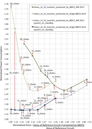
Fig. 4 presents the overhead results for the optimal sensor versions as well as the power reductions whether the sleep mode is active (i.e. system on standby). We can see in Fig. 4 that there are minimum points on the curves for sleep mode in off-state. Therefore, it allows finding the optimal number of monitored chains. Observe in Fig. 4 that, after 6 chains, lower the number of chains, higher the overheads since there are less transistors compounding the reference circuit. The optimal number of chains for both BBICS types is hence 6, and their design factors are Xn=2, Yn=6.2, Xp=2,
Yp=10.9, X=3 and Y=13.7. As the pull-up network
is always larger than the pull-down network in order to compensate the slower mobility of PMOS
Figure 4. Normalized power consumption and area for several reference circuits monitored by the optimal sensor versions
transistors, the design factor Yp has to be greater than Yn. Hence, the design factors of
Single-BBICS-2013 are also greater. Further, as a single sensor is
used to monitor both networks, its structure requires higher gain of amplification to balance the higher load on node1. Consequently, the offset on the bulk voltage is also higher, as seen in Fig. 5, leading to greater static power consumption especially due to the offset on PMOS bulk voltage. On the other hand, as the number of transistors is lower by using
Single-BBICS-2013, the power overhead achieves similar
results than BBICS_MR-2012 (about 26 %) and the area offset around 23 % against 38 % of
BBICS_MR-2012. Moreover, if sleep mode is active,
the power penalty is 15 % against 21 % of
BBICS_MR-2012. One could argue that an offset on
bulk voltage would reproduce noticeably change on threshold voltages of monitored gates and, thus, their timing characteristics would be altered. However simulation results show that the modifications in rise and fall time, and rise and fall delay of monitored
inverters are negligible. Therefore, no performance penalty is observed. Otherwise, as the sub-threshold leakage current is an exponential function of the threshold voltage, the static power consumption of monitored gates is significantly increased by around 17%. If sleep mode is active, the static power overhead is 7%.
Figure 5. Maximum NMOS bulk voltage and Minimum PMOS bulk voltage in function of the number of chains of 10 inverters protected by BBICS
V. CONCLUSIONS
This paper proposes a new BBICS presenting lower area than previous version and similar power overhead. In addition, it achieves lower sleep-mode power. With no performance penalty, this work allows identifying the optimal design factors of the sensor as well as the optimal number of monitored transistors to obtain the best trade-off between area and power. Furthermore, the results show that the offset on the NMOS bulk voltage is negligible for the optimal sensor versions. Ongoing works are the fabrication of a prototype and the validation of the approach using a laser beam to inject transient faults.
VI. REFERENCES
[1] E. H. Neto et al., “Using Bulk Built-in Current Sensors to Detect Soft Errors”, IEEE Micro, v. 26, n. 5, pp. 10–18, Sep. 2006.
[2] E. H. Neto et al., “Tbulk-BICS: A Built-In Current Sensor Robust to Process and Temperature Variations for Soft Error Detection”, IEEE Transactions on Nuclear Science, v. 55, n. 4, pp. 2281-2288, Aug. 2008. [3] F. S. Torres, R. P. Bastos, “Robust Modular Bulk Built-In Current
Sensors for Detection of Transient Faults”, in Proc. SBCCI, IEEE, 2012, pp. 1-6.
[4] R. P. Bastos et al., “Novel transient-fault detection circuit featuring enhanced bulk built-in current sensor with low-power sleep-mode”, Elsevier Microelectronics Reliability, v. 52, n. 9-10, pp. 1781-1786, Sep.-Oct. 2012.
[5] Z. Zhang et al., “A Bulk Built-In Voltage Sensor to Detect Physical Location of Single-Event Transients”, JETTA, Springer, March 2013. [6] A. Simionovski, G. Wirth, “Simulation Evaluation of an Implemented
Set of Complementary Bulk Built-In Current Sensors with Dynamic Storage Cell”, IEEE Transactions on Device and Materials Reliability, v. PP, n. 99, 2013.
[7] Predictive Technology Model (PTM) Web site: http://www.eas.asu.edu, last visited at June, 2011 (Nano-CMOS tool configured with default technology specifications).

![Figure 3. (a) Strucutres of a BBICS pair (NMOS and PMOS) proposed in [4]; and (b) the structure of our new single BBICS](https://thumb-eu.123doks.com/thumbv2/123doknet/12443338.335550/4.918.91.820.104.438/figure-strucutres-bbics-nmos-proposed-structure-single-bbics.webp)