Délivré par l’université Toulouse III – Paul Sabatier Discipline ou spécialité : Sciences et Génie des Matériaux
Co-tutelle avec l' Universidade Federal do Rio Grande Do Sul
Présentée et soutenue par Mônica Jung de Andrade Le 05 octobre 2010
Titre: STUDY OF ELECTRICAL PROPERTIES OF 2- AND 3-DIMENSIONAL CARBON NANOTUBES NETWORKS
Ecole doctorale : Sciences de la Matière Unités de Recherche : CIRIMAT Institut Carnot
JURY
S. BINOTTO FAGAN Professeur Centro Univ. Franciscano, UNIFRA Rapporteur K. MASENELLI-VARLOT Professeur Inst. Univ. France, INSA de Lyon Rapporteur C. de FRAGA MALFATTI Professeur Univ. Federal do Rio Grande Do Sul Examinateur
J.M. HOHEMBERGER Petróleo Brasileiro, PETROBRAS Examinateur L.A. FERREIRA COELHO Professeur Univ. do Estado de Santa Catarina Examinateur C.P. BERGMANN Professeur Univ. Federal do Rio Grande Do Sul Directeur de thèse A. PEIGNEY Professeur Université de Toulouse Directeur de thèse C. ESTOURNES Dir. Recherches CNRS, Toulouse Directeur de thèse
MINISTÉRIO DA EDUCAÇÃO
UNIVERSIDADE FEDERAL DO RIO GRANDE DO SUL
Escola de Engenharia
Programa de Pós-Graduação de Engenharia de Minas, Metalúrgica e de
Materiais – PPGE-3M
STUDY OF ELECTRICAL PROPERTIES OF 2- AND
3-DIMENSIONAL CARBON NANOTUBES NETWORKS
Mônica Jung de Andrade
Thesis in co-tutelle to obtain the title of Doctor in Engineering
Porto Alegre 2010
MINISTÉRIO DA EDUCAÇÃO
UNIVERSIDADE FEDERAL DO RIO GRANDE DO SUL
Escola de Engenharia
Programa de Pós-Graduação de Engenharia de Minas, Metalúrgica e de
Materiais – PPGEM
STUDY OF ELECTRICAL PROPERTIES OF 2- AND
3-DIMENSIONAL CARBON NANOTUBES NETWORKS
Mônica Jung de Andrade Mestre em Engenharia
Thesis presented to the Programa de Pós-Graduação em Engenharia de Minas, Metalúrgica e de Materiais – PPGE-3M, as part of the requirements to obtain the title of Doctor in Engineering.
Area of concentration: Science and Technology of Materials.
Porto Alegre 2010
This thesis was judged in order to obtain the title of Doctor in Engineering, in the area of Science and Technology of Materials and approved in its final format by the Thesis Advisor and Board of Examiners of the Course of Post-graduation.
Thesis Advisor at UFRGS (Brazil): Prof. Dr. Carlos Pérez Bergmann Thesis Advisor at UPS (France): Prof. Dr. Alain Peigney
Dr. Claude Estournès
Board of Examiners: Prof. Dr. Karine Masenelli-Varlot
Prof. Dr. Solange Binotto Fagan
Prof. Dr. Célia de Fraga Malfatti
Dr. João Marcos Hohemberger
Prof. Dr. Luiz Antônio Ferreira Coelho
Prof. Dr. Carlos Pérez Bergmann
ACKNOWLEDGMENTS
First of all, I am in really debt with my family and my boyfriend, who generously understood my abscences and supported me along all the period of this work even at separated continents for long periods. Even without knowing, they were many times my incentive to persue my dreams through their example of lifes and this work I dedicate to them.
I deeply acknowledge the opportunities of learning research with so many special people that generously received me in their laboratories and Universities:
Prof. Alain Peigney, Dr.Claude Estournès and Dr. Alicia Weibel for sharing their knowledge and teaching me that research need patience and persistence. Their scientific rigidity and attention along all the period at Université Paul Sabatier (Toulouse, France) and during the writing/correction of this manuscript greatly affected my formation and are acknowledged. Their criterious revising of this work favoured great improvements on it. I also acknowledge Prof. Alain Peigney and Dr. Alicia Weibel for the scanning electron microscope imaging.
Dr. Siegmar Roth for his enthusiasm for teaching science, culture and history. Dr. Viera Skakalova for her cherished endearment and concern. The nice moments at Max Planck Institut für Festkörperforschung (Stuttgart, Germany) with intercultural exchanges in the group and unequal opportunities given to develop ideas and discussions strongly contributed to my formation.
Prof. Carlos Pérez Bergmann, from Universidade Federal do Rio Grande do Sul (Porto Alegre, Brazil), to believe, support and incentive my work since undergraduate studies, giving no limits to the curious student with many dreams.
Thank you as well for all my friends and colleagues from Brazil and abroad for their support and nice environment of working: my colleagues at LACER and the multicultural families of the unforgettable 4C11 in Stuttgart and the brotherhood 0169 in Toulouse. I also thank all the technicians from Max Planck Institut für Festkörperforschung (Stuttgart, Germany) and from CIRIMAT/CNRS/Université Paul Sabatier (Toulouse, France) that helped me during many analyses and also in the spark-plasma sintering.
SUMMARY
LIST OF FIGURES...XV LIST OF TABLES ...XXI LIST OF ABBREVIATIONS...XXIII GLOSSARY ... XXVII ABSTRACT... XXIX RESUMÉ ... XXXI RESUMO... XXXIII 1 INTRODUCTION ... 35 1.1 JUSTIFICATIVE ... 39 2 OBJECTIVE ... 41 2.1 GENERAL OBJECTIVE ... 41 2.2 SPECIFIC OBJECTIVES ... 41
3 LIMITATIONS OF THE RESEARCH WORK... 43
4 BIBLIOGRAPHIC REVISION... 45
4.1 CNT - STRUCTURE, TYPE, SYNTHESIS AND CHARACTERIZATION... 45
4.1.1 Structure and types of carbon nanotubes ... 45
4.1.2 Synthesis of carbon nanotubes ... 47
4.1.3 Characterization of carbon nanotubes and its networks ... 51
4.2 PRODUCTION OF 2D AND 3D CNTNS... 56 4.2.1 2D CNTNs ... 56 4.2.2 3D CNTNs in insulator matrices ... 58 4.3 CNTS-SIO2 NANOCOMPOSITES... 59 4.3.1 Dispersion... 59 4.3.2 Densification ... 60 4.3.3 SPS method... 61
4.4 ELECTRICAL PROPERTIES OF CARBON NANOTUBES AND ITS NETWORKS... 63
4.4.1 Intrinsic properties of CNTs affecting their electrical conductivity ... 66
4.4.2 Properties of CNTNs affecting the electrical conductivity... 70
5 MATERIALS AND METHODS ... 79
5.1 CARBON NANOTUBES... 79
5.1.1 Commercial CNTs ... 79
5.1.2 Synthesis and extraction of DWCNT ... 80
5.2 PRODUCTION OF CNTNS IN 2D AND 3D SYSTEMS... 81
5.2.1 Two dimensional systems ... 81
5.2.2 Three dimensional systems ... 84
5.3 CHARACTERIZATION METHODS... 87
5.3.1 Spectroscopic and optical characterizations ... 88
5.3.2 Zeta potential ... 89
5.3.3 Electron and Atomic Force Microscopies ... 89
5.3.4 Electrical conductivity and properties of percolation ... 90
5.3.5 Carbon content ... 93
5.3.6 Specific surface area ... 93
5.3.7 Density determination ... 93
5.3.8 X-ray diffraction... 94
6 RESULTS AND DISCUSSIONS ... 95
6.1 CHARACTERIZATION OF CNTS... 95
6.1.1 Summary of characterization of the commercial CNTs ... 108
6.2 CNTNS IN 2D SYSTEM... 110
6.3 CNTNS IN 3D SYSTEM: DWCNT-SIO2 NANOCOMPOSITES... 119
6.3.1 DWCNTs synthesis and characterization ... 119
6.3.2 DWCNTs Functionalization ... 130
6.3.3 Nanocomposite powders ... 145
6.3.4 Dense F-DWCNT-SiO2 Nanocomposites ... 150
6.3.5 Summary of 3D CNTNs ... 187
CONCLUSIONS ... 193
ATTACHMENTS ... 196
LIST OF FIGURES
Figure 4.1 (A) Vectors
→
h
C
and
→
T defined by the indices (n,m) [52]; (B) the three different structures of CNTs: armchair, zigzag and chiral...47 Figure 4.2 Typical Raman spectrum from SWCNT bundles. ...52 Figure 4.3 Schematic diagram of a CNTN immersed into a matrix: (A) with good
compatibility with the matrix and fully densified; (B) with good compatibility with the matrix, but with remaining porosity; (C) with bad interface interaction with the matrix and non-ideally dispersed...60 Figure 4.4 Schematic diagram of SPS device. ...62 Figure 4.5 Pathway of CNTs connected, where Lce is the equivalent straight length of
each CNT, Lp is the length of the connected CNTs path and Lpe is the equivalent length of the CNTs path [35]. ...67 Figure 4.6 Schematic representation of the CNT structure after an oxidation process. ...70 Figure 4.7 Schematic diagram of interacting CNTs bundles in a γ angle (top) and in
parallel (bottom), where LB and dB are the length and width of the bundles [150]. ...75 Figure 5.1 Schematic diagram of the post-growth techniques used in this work to
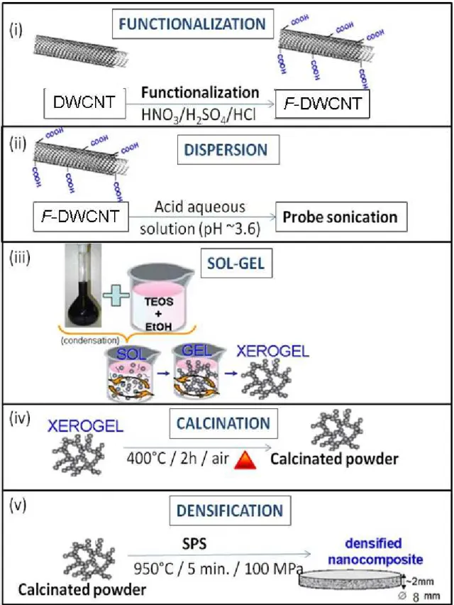
prepare 2D CNTNs: spray-coating, dip-coating, filtration method and electrophoretic deposition. ...83 Figure 5.2 Schematic diagram of the steps for the preparation of 3D CNTNs using F-DWCNTs embedded in silica matrix SiO2: (i) functionalization of DWCNTs; (ii) dispersion of the F-DWCNTs into acid aqueous solution with the aid of probe sonication; (iii) in-situ production of silica (precursor: tetraethylorthosilicate, TEOS) over F-DWCNTs through organic sol-gel route; (iv) calcination of the nanocomposite xerogel; (v) densification of the calcinated powder through spark-plasma sintering (SPS)...85 Figure 5.3 Schematic diagram of the overall experimental procedure to produce
CNTNs in 2D (spray-coating, dip-coating, filtration method and electrophoretic deposition) and 3D - in liquid with chloroform or in silica prepared by sol-gel and densified by spark-plasma sintering (SPS)...88 Figure 5.4 Schematic diagram of apparatus used for electrical measurements of (a)
3D CNTNs in a liquid electric insulator matrix; (b) 2D CNTNs; (c) 3D CNTNs embedded in silica matrix...91 Figure 5.5 Configuration for the electrical conductivity measurements of CNTNs in 2D
systems using Pd/Au (200/2000 Å) electrodes that were deposited by the technical service of Max Planck Institute for Solid State Research. ...92 Figure 6.1 TEM micrographs of SWCNT (mainly gathered in bundles). Black arrows
Figure 6.2 TEM micrographs of (A) MWCNT-I and (B) MWCNT-I-short: Red arrows as defects, black arrows as other carbon impurities and blue arrows as metal NPs. ...96 Figure 6.3 TEM micrographs of MWCNT-II: Red arrows/circle as defects, black
arrows as other carbon impurities and blue arrows as metal NPs...96 Figure 6.4 Raman spectra of CNTs at λ = 632.8 nm (normalized to D*): (A) SWCNT
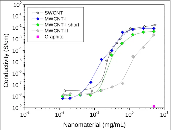
(inset: RBM); (B) MWCNT-I, MWCNT-I-short, MWCNT-II and graphite. ...98 Figure 6.5 Electrical conductivity of the carbon suspensions in chloroform at 1.5 V
DC (0.104 V/cm) during sonication: carbon content (mg/mL) versus electrical conductivity. Both in logarithmic scale...101 Figure 6.6 Electrical conductivity of the carbon suspensions in chloroform at 1.5 V
DC (0.104 V/cm) during sonication: vol.% of nanomaterial (log scale) versus electrical conductivity (log scale). Inset: vol.% of nanomaterial (linear scale)
versus electrical conductivity (log scale). ...102
Figure 6.7 Conductivity versus reduced volume for HiPco SWCNTs (both in logarithmic scale). Below 1 mg/mL of CNTs (reduced volume = 3.7) the conductivity follows a linear correlation. The CNT concentration (mg/mL) is indicated for each point. ...105 Figure 6.8 Measured conductivities of HiPco SWCNT dynamic 3D CNTNs in
chloroform in comparison to calculated conductivities by modified rule of mixtures considering an aspect ratio (L/d) of 7000 and β=0.2...106 Figure 6.9 Surface resistance (log scale) versus transmittance of a commercial ITO
and other data from literature [136] in comparison to several CNTNs prepared through different techniques using similar material of literature (HiPco SWCNTs): dip-coating (DC), filtration method (FM), spray-coating (SC) and electrophoretic deposition (ED). Eye-guide auxiliary line to visualize the tendency...111 Figure 6.10 FESEM micrograph at 25 kx of magnification of a dip-coated CNTN (red
arrow: CNT loop). ...112 Figure 6.11 Transmittance (%) versus concentration per area of several CNTNs
prepared through different techniques with HiPco SWCNTs in comparison with other data from literature using similar material [136]. ...113 Figure 6.12 Surface conductance (log scale) versus concentration per area of several
CNTNs prepared through different techniques with HiPco SWCNTs in comparison with other data from literature using similar material [136]...113 Figure 6.13 Surface conductance (log scale) versus reduced concentration (log
scale) of several CNTNs prepared through different techniques with HiPco SWCNTs in comparison with other data from literature using similar material [136]. Inset: Power law fitting of the surface conductance (log scale) of SWCNT random 2D networks versus reduced concentration to obtain the constant of dimensionality. ...114 Figure 6.14 Schematic diagram (note: CNTs and surfactant are not in the real
proportions) of the effect in the electrical conductivity of CNTNs with and without
surfactant. ...115 Figure 6.15 Surface resistance (log scale) versus transmittance of the pioneer work
in comparison to the CNTNs prepared by filtration method (FM) using different commercial CCVD CNTs: HiPco SWCNT, DWCNT-I and MWCNT-I...117 Figure 6.16 Possible applications for ultrathin CNTNs produced in this work (based
on [136]). ...118 Figure 6.17 XRD patterns from DWCNTs: (A) before and (B) after extraction of
magnesia (DWCNT), with an inset (C) of the filtrated solution after extraction with chloridric acid. ...121 Figure 6.18 TEM micrographs of home-made DWCNTs after extraction with HCl. Red
arrows as defects (“kinks”) and blue arrows as metal NPs...122 Figure 6.19 Raman spectra at different regions from DWCNT-C (DWCNT sample
with the highest average ID/G: 17%). Inset left: RBM spectra at different regions (coloured lines) and average RBM (black line). Inset right: average Raman spectrum. ...124 Figure 6.20 Electrical conductivity of the carbon suspensions (volume percent) in
chloroform at 1.5 V DC (0.104 V/cm) during sonication (dynamic network) of different batches of DWCNTs...126 Figure 6.21 Measured conductivities of DWCNT-E dynamic 3D CNTNs (used for wet
route) in chloroform in comparison to calculated conductivities (modified rule of mixtures) considering an aspect ratio (L/d) of 23300. ...128 Figure 6.22 Conductivity versus reduced volume for DWCNT-E (both in logarithmic
scale). The CNT concentration (mg/mL) is indicated for each point...129 Figure 6.23 Zeta potential curve of CNTs non-functionalized (DWCNTs) and
functionalized (using a reflux step) with acid nitric (F-DWCNTs/HNO3), with acids nitric and sulphuric (F-DWCNTs/HNO3/2SO4) and with acids nitric, sulphuric and chloridric (F-DWCNTs/HNO3/H2SO4/HCl). ...131 Figure 6.24 Qualitative stability test at pH 3.6 for functionalization with HNO3/H2SO4 -HCl (aqueous suspension with ~1 mg/mL) at different times: T0 is just after preparation of suspension, T1 is after 24h, T2 is after 48h and T3 is after one week...133 Figure 6.25 F-DWCNT: (a) XRD pattern of the material after rinsing with deionized
water and (b) first filtrated solution after the chemical oxidation step. ...134 Figure 6.26 TEM images of (a) F-DWCNT-B and (b) F-DWCNT-E (material used for
wet route). Red arrows as defects (“kinks”), black arrows as other carbon impurities and blue arrows as metal NPs. ...135 Figure 6.27 Average Raman spectra at λ = 632.8 nm (normalized to D*) of F-DWCNT
samples from different batches in comparison to original material. Inset: upshift in D* after functionalization...137 Figure 6.27 (Continued) ...138 Figure 6.28 Normalized (by the mass and then by C=C peak at ~1630cm-1) Infrared
spectra of DWCNTs-II before (black line) and after (red line) chemical oxidation from (a) DWCNTs-E, (b) DWCNTs-B and (c) DWCNTs-C. ...141 Figure 6.29 Electrical conductivity of the carbon suspensions in chloroform at 1.5 V
stove (F-DWCNT-B and F-DWCNT-C) and dried in dessicator (F-DWCNT-D and F-DWCNT-E)...143 Figure 6.30 FESEM image of a nanocomposite powders D (a) and W (b) prepared
using dry (2.97 vol.% of average carbon content) or wet (6.43 vol.% of average carbon content) DWCNTs, respectivelly...147 Figure 6.31 Raman spectra at λ = 632.8 nm (normalized to D*) of a nanocomposite
powder obtained by (A) dry route and (B) wet route (containing 6.43 vol.% of carbon): coloured lines are spectra from different regions of the same sample and black line is the average spectra. ...149 Figure 6.32 SPS parameters used to densify the W set of nanocomposites. Inset:
electric current applied during SPS densification. ...157 Figure 6.33 Raman spectra at λ = 632.8 nm normalized by G band done in different
regions of the sample (coloured lines as inset) for each sample from dry route: (a) D1 (0.22 wt.%); (b) D2 (0.22 wt.%); (c) D3 (0.22 wt.%); (d) D4 (0.29 wt.%); (e) D5 (2.44 wt.%). Black line: Average Raman spectra of the respective densified F-DWCNT-SiO2 nanocomposites...160 Figure 6.33 (Continued) ...161 Figure 6.33 (Continued) ...162 Figure 6.34 Raman spectra at λ = 632.8 nm normalized by G band done in different
regions of the sample (colored lines as inset) for each sample from wet route: (a) W2 (0.15 wt.%); (b) W3 (0.47 wt.%); (c) W4 (0.48 wt.%); (d) W6 (5.32 wt.%). Average Raman (black line) spectra of samples from respective densified F-DWCNT-SiO2 nanocomposites. ...164 Figure 6.35 FESEM image of a fractured surface of F-DWCNT-SiO2 nanocomposite
obtained by dry route: (a,b) sample D1 (0.22 wt.%); (c) sample D2 (0.22 wt.%); (d) sample D3 (0.22 wt.%); (e,f) sample D4 (0.29 wt.%); (g,h) sample D5 (2.44 wt.%). ...167 Figure 6.36 (A) FESEM image of a fractured surface of F-DWCNT-SiO2 (0.29 wt.% of
carbon)nanocomposite obtained by dry route; (B) Evidence of wettability of the
F-DWCNT by the silica matrix. ...168
Figure 6.37 FESEM images of the fracture surface of F-DWCNT-SiO2 nanocomposites obtained through the wet route: (a) sample W1 (0.12 wt.%); (b) sample W3 (0.47 wt.%);(c,d) sample W4 (0.48 wt.%); (e,f) sample W5 (1.27 wt.%); (g,h) sample W6 (5.32 wt.%). ...172 Figure 6.38 Electrical conductivity measured for the F-DWCNT-silica nanocomposites
(D and W series) measured by two-probe method...177 Figure 6.39 Electrical conductivity measured for the F-DWCNT-silica nanocomposites
measured by two-probe method (straight line below) in comparison to expected from modified rule of mixtures (dash-dot line above) using a L/d=23300 and β=0.2 (Equation 4.13b) and its probability of percolation (Equation 4.2), considering critical volume fraction (ФCVF) of F-DWCNT measured by dynamic
percolation (0.003 vol.%)...179 Figure 6.40 (A) Electrical conductivity versus various CNT content (vol.%) for CNT-ceramic nanocomposites (non-aligned CNTNs) in insulator matrices (note:
respectively [98]): F-DWCNT-SiO2 nanocomposites from this work in comparison with data from literature [29,30,94,99,100b,126,190-196,199,200]. (B) Same enlarged graph for the low contents. ...186 Figure 0.1 Schematic diagram of the molecule of sodium dodecyl sulfate, SDS...196 Figure 0.2 Typical spectral transmission including Fresnel reflection loss. The
uppermost nearly straight line indicates the calculated Fresnel reflection loss of two uncoated surfaces. Path length of 10 mm. ...197 Figure 0.3 Schematic diagram of the reaction of silanization of the surface of silica
glass substrate by reacting with 3.Aminopropyltriethoxysilan (APS). ...197 Figure 0.4 Schematic diagram of the reaction of silanization of the surface of silica
glass substrate by reacting with 3.Aminopropyltriethoxysilan (APS). ...198 Figure 0.5 Normalized electrical conductivity (~1 mg/mL) of the carbon suspensions
in chloroform at 1.5 V DC (0.104 V/cm) during sonication of HiPco-SWCNT and DWCNT along time. ...199 Figure 0.6 Conductivity of MWCNT-I suspensions in chloroform versus its reduced
volume (both in logarithmic scale). The CNT concentration (mg/mL) is indicated for each point. ...199 Figure 0.7 Conductivity of MWCNT-I-short suspensions in chloroform versus its
reduced volume (both in logarithmic scale). The CNT concentration (mg/mL) is indicated for each point. ...200 Figure 0.8 Conductivity of MWCNT-II suspensions in chloroform versus its reduced
volume (both in logarithmic scale). The CNT concentration (mg/mL) is indicated for each point. ...200 Figure 0.9 (A) AFM image (height data type with Z range of 30 nm) evidence of
alignment of dip-coating first adsorbed layer (blue arrow is the direction of dipping and black arrow shows CNT loop); (B) and increase of bundling with number of dippings...201 Figure 0.10 Infrared spectra of KBr pill without CNTs. ...202 Figure 0.11 XRD pattern of a pure silica sample with apparent slight beginning of
crystallization (black arrow). ...202 Figure 0.12 XRD patterns of the F-DWCNT-SiO2 materials after consolidation by SPS
LIST OF TABLES
Table 1.1 Main properties of individual CNTs...36 Table 4.1 Examples of carbon structures with different aspect ratio and their
percolation as 3D network in insulator matrices. ...65 Table 5.1 Main characteristics of the commercial CNTs given by the producers:
aspect ratio measured by producers (TEM and SEM), carbon content wt.% (measured by thermal gravimetric analysis, TGA under air, or elementary analysis, EA) and other impurities (not mentioned or by ICP, inductively coupled plasma) ...80 Table 6.1 Main characteristics of the CNTs studied in this work: carbon content wt.%
(measured by flash-combustion method or informed by producer that measured by thermal gravimetric analysis or elementary analysis), aspect ratio measured by producers (TEM and SEM) and calculated D/G ratios measured by Raman spectroscopy ( λ = 632 nm) for the carbon materials in comparison with a graphite. ...99 Table 6.2 Observed aspect ratios for various commercial carbon materials, in
comparison to the calculated aspect ratios through the observed critical volume. ...104 Table 6.3 Electrical conductivity of free standing papers produced from different
carbon materials, compared with the same materials’ conductivities in liquid medium in the dynamic mode, at the highest concentration measured (around 5 mg/mL). ...108 Table 6.4 Comparison of the average roughnesses of commercial ITO over glass
with CNTNs using HiPco SWCNTs and prepared by different techniques (all with similar transparency, around 85 % at 550 nm): dip-coating (DC), filtration method (FM), spray-coating (SC) and electrophoretic deposition (ED). Size of each analyzed area: 210.25 µm2. ...116 Table 6.5 Main characteristics of the DWCNTs studied in this work: average carbon
content wt.% (measured by flash-combustion method: two measurements for each sample) and calculated D/G ratios measured by Raman spectroscopy ( λ = 632 nm) for the carbon materials in comparison with a graphite. ...125 Table 6.6 Main characteristics of the DWCNTs after their functionalization: average
carbon content wt.% (measured by flash-combustion method: two measurements for each sample) and average ID/G ratios measured by Raman spectroscopy ( λ = 632 nm) for the carbon materials in comparison to original material. ...139 Table 6.7 Examples of studies of sintering parameters by SPS with pure silica: silica
powder, SPS parameters, final density by Archimedes, relative density (considering amorphous silica) and general aspect. ...153 Table 6.8 Densities of F-DWCNT silica nanocomposites measured by Archimedes
method with their statistic deviation between brackets in comparison to their SPS parameters, carbon content and relative density (by considering full silica amorphous). ...156
Table 6.9 D and W samples microstructural analysis (selected only “clean” type of fracture for these analyses)...171 Table 6.10 Electrical conductivity of F-DWCNT-SiO2 nanocomposites obtained by the
dry (D samples) and wet (W samples) routes measured by two-probe method. ...174 Table 0.1 Main characteristics of substrate used for the deposition of 2D CNTNs..196
LIST OF ABBREVIATIONS
CNT(s) Carbon nanotube(s). CNF(s) Carbon nanofiber(s).
SWCNT(s) Single-walled Carbon nanotube(s). DWCNT(s) Double-walled Carbon nanotube(s). MWCNT(s) Multi-walled Carbon nanotube(s). CNTN(s) Carbon nanotubes network(s).
2D Two-dimensional
3D Three-dimensional
vol.% Volume per cent
wt.% Weight per cent
(C)CVD (Catalytical) Chemical Vapor Deposition. NP(s) Nanoparticle(s). θ Chiral angle. → h C Chiral vector. →
T Translational symmetry vector (parallel to tube axis).
→
1
a and a→2 Unit vectors of the graphene.
RBM Radial Breathing mode.
D “Diamond” or “defect” mode.
G Tangential mode.
D* D*-band also known as second order G’-band; overtone
of D mode.
ID/G Ratio between the intensities of D and G modes.
TGA Thermogravimetric analysis.
EA Elementary analysis.
AFM Atomic force microscopy.
(HR)TEM (High Resolution) Transmission Electron Microscopy. (FE)SEM (Field Emission) Scanning Electron Microscopy. FTIR Fourier Transform Infrared Spectroscopy.
ICP Inductively Coupled Plasma
Cn Carbon content in weight per cent.
SG Specific gravity.
W Weight of the sample. Subscripts air and water refer to the measurement in air and in water, respectively.
XRD X-ray diffraction.
PU Polyurethane.
PC Polycarbonate.
PI Polyimide.
PET Poly(ethylene terephthalate). PVDF Poly(vinylidene fluoride).
HiPco High Pressure Carbon Monoxide.
SDS Sodium dodecyl sulphate.
F-CNT(s) Functionalized Carbon nanotube(s). TEOS Tetraethyorthosilicate.
r Molar ratio of water per tetraethylorthosilicate.
ITO Indium tin oxide (solid solution of 90% In2O3 and 10% SnO2 by weight).
SC Spray-coating.
ED Electrophoretic deposition.
FM Filtration method.
SPS Spark-Plasma Sintering.
HIP High-pressure cold quasi-isostatic pressing.
HP Hot-pressing.
ξ Probability at which CNTs percolate.
ФCVF (ACAF) Volume (area) fraction of carbon nanotubes in which the
percolation process begins (also called critical volume fraction).
ФF (AF) Volume (area) fraction of carbon nanotubes.
PCNT Carbon nanotubes density per area (CNT/µm
2 ).
C CNT
P Critical carbon nanotubes density per area (CNT/µm
2 ).
σ (R) Electrical conductivity (resistivity). Subscripts C, M and F
refer to the composite, matrix and filler (in this case, CNTs), respectively.
σ0 (R 0) Constant of proportionality: electrical conductivity
(resistivity) of the filler.
σMAX Maximal electrical conductivity.
V Volume of electrical conductive “fillers” “(in this case, the carbon nanotubes).
τ Critical exponent that represents the dimensionality of the network.
Vex Total excluded volume. For randomly oriented infinitely
thin cylinders it gives a value of 1.4.
Ve Excluded volume.
Nc Critical number density of objects in the system.
D Diameter of the filler.
L Length of the filler.
LAV Average length of bundles.
Lce Equivalent straight length of each CNT.
Lp Length of the connected CNTs path.
Lpe Equivalent length of the CNTs path.
β Parameter depends on the orientation of the filler and it is 0.2 if it is a random orientation in a tridimensional volume and considered as 0.35 if its orientation is randomic in the two dimensional plane.
α Parameter depends on the dimensions of the filler and can be calculated by Equation 0.1.
H Distance between the electrodes.
A Area of the electrodes.
W Length of the electrodes.
RS Surface (or sheet) resistance (or resistivity).
T Optical transmittance of the network.
αCNT Absorbance coefficient (whose value is 2.875 x 10⁻⁶µm2
for a light wavelength of 550 nm, assuming CNTs with 0.5 µm length and diameter of 1.2 nm).
ρARCHIMEDES Archimedes density.
ρGEOMETRICAL Geometrical density.
Agg Parameter of dispersity related to the size and frequency of aggregates.
GLOSSARY
Nanoscale At least one dimensional scale in the order of
nanometer (10-9 meters).
Bundles Integral number N of carbon nanotubes aligned parallel
to a common axis, which is termed the bundle axis.
Aggregates Bundles of carbon nanotubes held together in an disorderly manner.
Buckypaper Self-standing papers of carbon nanotubes by filtering a solution containing carbon nanotubes, which leads to a compaction of the carbon nanotubes.
Surface resistance In plane resistance of a square ( ) with contacts at opposite sides, unit is Ω/sq (sometimes Ω/ or Ω or Ωsq). Sometimes the term surface (or sheet) resistivity is used in literature instead of surface (or sheet) resistance.
Ohms per square Is an alternate common unit (generally denoted “Ω/sq”), which is dimensionally equal to an Ohm, but is exclusively used for sheet resistance. This is an advantage, because a sheet resistance of "1Ω" could be taken out of context and misinterpreted as a bulk resistance of 1 Ohm, while a sheet resistance of "1Ω/sq" cannot be so misinterpreted. The reason for the name "Ohms per square" is that a square sheet with sheet resistance 1 Ohm/square has an actual resistance of 1 Ohm, regardless of the size of the square. (For a square, L = W, so RS = R.) The unit can
be thought of as, loosely, "Ohms per aspect ratio".
Kinks Atomic-scale deviations from the perfect hexagonal
lattice of carbon nanotubes (CNTs) manifest themselves as ‘kinks’ at the junctions between
nanotube portions of different diameters. Under certain growth conditions, MWNTs exhibit helical, coil or zig-zag morphologies with kinks connecting adjacent segments, leading to a curvature in the CNT.
ABSTRACT
Two and three dimensional carbon nanotube networks (2D- and 3D-CNTNs) were prepared over silica glass substrate and in silica matrix, respectively. Several types of CNTs (single-, double- and multi-walled carbon nanotubes, SWCNTs, DWCNTs and MWCNTs, respectively) were characterized by transmission electron microscopy, Raman spectroscopy and carbon analysis, while their aptitudes to form a percolating network were compared by measurement of their electrical conductivity in dynamic suspensions in chloroform. The conductivity of SWCNTs and DWCNTs suspensions well follow the power law of the percolation theory, with an exponent close to the theoretical value of a 3D network. The SWCNTs suspensions present the higher maximum normalized conductivity (3.08 S.cm2/g) whereas the DWCNTs suspensions present the lower percolation thresholds (0.002-0.06 vol.%) which led to choose SWCNTs for the preparation of 2D-CNTNs and DWCNTs for the preparation of CNT-silica nanocomposites (3D-CNTNs).
To produce 2D-CNTNs, SWCNTs aqueous suspensions containing sodium dodecyl sulphate were deposited over amorphous silica substrates using four different techniques : dip-coating, filtration, spray-coating and electrophoretic deposition. Most of the 2D-CNTNs formed a percolating network whose electrical conductivity well followed the power law, with an exponent around 1.29, which is in agreement with theoretical predictions. Dip-coating and electrophoretic deposition provided the smoothest CNTNs and might be an interesting option for solar cell applications. The obtained characteristics of surface conductance and transparency in the UV also demonstrated their possible applications in displays, touch screens, shielding in cathode tubes and electrostatic dissipation.
CNT-silica matrix nanocomposites (3D-CNTNs) were prepared by the sol-gel route, using DWCNTs which were previously submitted to a mild functionalization, their dispersion being carried out by probe sonication. The materials were fully densified by spark-plasma sintering. The dispersion state of CNTs was evaluated by field emission scanning electron microscopy and correlated with the electrical properties. The comparison of two variations in the preparation route (ie: the DWCNT were dried or not after their functionnalization) led to a good correlation between the dispersions states (presence and size of CNTs aggregates) and the percolation thresholds. For the “Dry” route, the percolation operates at only 0.35 vol.% DWCNT, which is lower that the values reported for CNT-silica nanocomposites. For the “Wet” one, the more conductive material shows an electrical conductivity (1.56 S/cm) higher than the values reported for similar materials. In spite that the dispersion of CNTS could be still improved, the achieved electrical conductivity of these nanocomposites is still high enough for their use in antielectrostatic or heating applications.
RESUMÉ
Des réseaux de nanotubes de carbone (CNTs) en deux ou trois dimensions (2D- et 3D-CNTNs) ont été préparés respectivement sur substrat de silice amorphe et dans une matrice silice. Plusieurs types de CNTs (mono-, double- et multi-parois, respectivement SWCNTs, DWCNTs et MWCNTs) ont été caractérisés par microscopie électronique à transmission, spectroscopie Raman et analyse élémentaire du carbone, et leurs aptitudes à former un réseau percolant ont été comparées par mesure de la conductivité électrique de suspensions dynamiques de ces CNTs dans le chloroforme. La conductivité des suspensions de SWCNTs et de DWCNTs obéit à la loi de puissance de la théorie de percolation, avec un exposant proche de la valeur théorique d'un réseau 3D. Celle des suspensions de SWCNTs présentent une conductivité normalisée maximale (3.08 S.cm2/g) tandis que celle des suspensions de DWCNTs présente le plus faible seuil de percolation (0.002-0.06 vol.%) ce qui a conduit à choisir les SWCNTs pour la préparation des 2D-CNTNs et les DWCNTs pour la préparation des nanocomposites CNT-silice (3D CNTNs).
Les 2D-CNTNs ont été préparés par dépôt de suspensions aqueuses de SWCNTs contenant du dodecyl sulfate de sodium sur de la silice amorphe, par quatre techniques différentes: trempage, filtration, spray et dépôt électrophorétique. Les 2D-CNTNs forment un réseau percolant dont la conductivité électrique obéit à la loi de puissance, avec un exposant d'environ 1.29, ce qui en en bon accord avec les prédictions théoriques. Les dépôts effectués par trempage et les dépôts électrophorétiques conduisent aux films les plus lisses et peuvent constituer une option intéressante pour des applications dans les cellules solaires. La conductance de surface et la transparence obtenues dans l'UV laissent espérer des applications possibles dans les écrans d'affichage, les écrans tactiles, les tubes cathodiques et les films destinés à dissiper les charges électrostatiques.
Les nanocomposites CNT-silice (3D-CNTNs) ont été préparés par sol-gel, en utilisant des DWCNTs qui furent d'abord soumis à un traitement doux de fonctionnalisation, leur dispersion étant réalisée par sonication avec une sonde. Les matériaux ont été ensuite complétement densifiés par "spark-plasma sintering". Les états de dispersion des CNTs ont été évalués par microscopie électronique à balayage à émission de champ et corrélé aux propriétés lectriques. La comparaison de deux variantes de la méthode de préparation (i.e.: DWCNT séchés ou non séchés après leur functionnalisation) a conduit à une bonne corrélation entre les états de dispersion (présence et taille des aggregats de CNTs) et les seuils de percolation. Pour la voie sèche, la percolation intervient pour seulement 0.35 vol.% DWCNT, ce qui est plus faible que les valeurs publiés pour les nanocomposites CNT-silice. Pour la voie humide, le matériau le plus conducteur présente une conductivité électrique (1.56 S/cm) plus élevée que celles publiés pour des matériaux similaires. Bien que l'état de dispersion des CNTs puisse encore être amélioré, la conductivité électrique obtenue pour ces nanocomposites est déjà suffisamment élevée pour leur utilisation pour évacuer les charges électrostatiques ou comme éléments chauffants.
RESUMO
Redes bi- e tridimensionais de nanotubos de carbono (2D e 3D-RNTCs) foram preparadas sobre substratos de vidro de sílica e em matriz de sílica, respectivamente. Vários tipos de nanotubos de carbono (nanotubos de carbono de paredes simples, dupla e multicamadas, NTCPSs, NTPDs e NTPMs respectivamente) foram caracterizados por microscopia eletrônica de transmissão, espectroscopia Raman e análise de carbono, enquanto que as suas aptidões para formar uma rede de percolação foram comparadas através da medição da suas condutividades elétricas em suspensões dinâmicas em clorofórmio. A condutividade das suspensões de NTCPSs e NTCPDs seguiram a lei de potência da teoria de percolação, com expoente próximo ao valor teórico de uma rede 3D. As suspensões de NTCPSs apresentaram 3.08 S.cm2/g), enquanto que as suspensões de NTCPDs apresentaram o menor teor crítico para percolação (0.002-0.06% vol.) o que levou a escolher NTCPSs para a preparação de 2D-RNTCs e NTCPDs para a preparação de nanocompósitos CNT-sílica (3D-RNTCs).
Para produzir em 2D-RNTCs, suspensões aquosas de NTCPSs contendo dodecil sulfato de sódio foram depositadas sobre substratos de sílica amorfa utilizando quatro diferentes técnicas: dip-coating, filtração, deposição por spray e deposição eletroforética. A maioria das 2D-RNTCs formaram uma rede de percolação cuja condutividade elétrica também seguiu a lei de potência, com expoente em torno de 1.29, que está de acordo com as previsões teóricas. Dip-coating e deposição eletroforética resultaram nas mais suaves RNTCs sendo uma opção interessante para aplicações em células solares. As características obtidas de condutância de superfície e de transparência no UV também demonstraram suas possíveis aplicações em displays, telas de toque, blindagem em tubos catódicos e dissipação eletrostática.
Nanocompósitos de NTCs em matriz de sílica (3D-RNTCs) foram preparados pela rota sol-gel, utilizando NTCPDs que foram previamente submetidos a uma funcionalização branda e sua dispersão foi realizada com ultrassom de ponta. Os materiais foram totalmente densificados por spark-plasma sintering. O estado de dispersão dos nanotubos de carbono foi avaliado por microscopia eletrônica de varredura por emissão de campo e correlacionados com as propriedades elétricas. A comparação das duas variações na rota de preparação (ou seja: os NTCPDs foram secos ou não após a sua funcionalização) levou a uma boa correlação entre os estados dispersões (presença e tamanho dos agregados de NTCs) e os pontos críticos de percolação. Para a rota "seca", a percolação opera em apenas 0.35 vol. % de NTCPDs, que é inferior aos valores reportados para nanocompósitos de sílica contendo NTCs. Para a rota "úmida", o material mais condutor apresenta uma condutividade elétrica (1.56 S/cm) maior do que o relatado por materiais similares. Apesar de que a dispersão de NTCs poderia ser ainda melhor, as condutividades elétricas obtidas destes nanocompósitos já são altas o suficiente para seu uso em elementos de aquecimento ou antieletrostáticos.
1 INTRODUCTION
Carbon nanotubes (CNTs) have unique physical and chemical properties (as summarized in Table 1.1), yielding more than 60000 publications in the last 19 years (according to Science Citation Index, ISI).
Already in 1952 Radushkevich and Lukyanovich presented in a soviet journal called Journal of Physical Chemistry [1] several transmission electron microscopy (TEM) images from some tubular nanostructures made of carbon, whose diameter was around 50 nm. However, probably due to “cold war” and to limitations of access to soviet publications, this report was ignored by others researchers. Even though it is possible that CNTs have been produced from vapor phase using methane as carbon source [2] before the soviets, CNTs could not be visualized since TEM was not invented on that period yet. Twenty four years after the soviets, Oberlin, Endo and Koyama also showed TEM images of hollow carbon structures produced by chemical vapor deposition [3]. In 1979, Abrahamson, Wiles and Rhoades also presented evidences of production of hollow carbon filaments by arc discharge using carbon electrodes in a nitrogen atmosphere at low pressure during the 14° Biennial Conference on Carbon at Penn State University [4]. In 1987, a patent was registered in USA by Howard G. Tennent for Hyperion Catalysis for the production of “cylindrical discrete carbon fibril” with constant diameter between 3.5 and 70 nm and length about 102 times the diameter, with an outer region of multiple essentially continuous layers of ordered carbon atoms and a distinct inner core region, each of the layers and core disposed substantially concentrically about the cylindrical axis of the fibril [5]. However, it was only after Iijima published in 1991 about CNTs showing high resolution transmission electron microscopy images (HRTEM) and their interpretation as fringes of cylindrical and concentrical curved graphene walls of multi-walled carbon nanotubes (MWCNTs) [6] that many scientists focused their work on CNTs research.
The most used technique for the synthesis of CNTs is catalytical chemical vapor deposition (CCVD) since it allows the large scale production of CNTs and low-cost processes, which permits their further applications. Most of the commercial producers of CNTs have been using this technique.
Table 1.1 Main properties of individual CNTs.
Aspect ratio
Length of nanometers to centimeters [7], but usually in the order of micrometers.
Diameter can range from 0.4 nm [7,8] to 100 nm [9,10], but usually is between 1 nm to 20 nm [7].
Electrical conductivity
Metallic (ballistic transport), semiconducting p-, n-doped or ambipolar [7].
Operating current density ~ 109 A/cm2 (Cu~ 106 A/cm2) [7]
Thermal conductivity
~ 6000 W.K-1m-1 (single-walled carbon nanotubes, SWCNTs) to 3000 W.K-1m-1 (multi-walled carbon nanotubes, MWCNTs) along the axis (Cu~ 400 W.K-1m-1) [7]
Specific surface area 100-1300 m2/g for closed CNTs [11] Specific gravity 0.5-3 g.cm-3 [12]
Mechanical property
E ~ 640 GPa (SWCNTs) - 1060 GPa (MWCNTs) [7]
σ ~ 23 - 63 GPa (tensile strength of double-walled carbon nanotubes, DWCNTs) [7]
Chemical property Chemically inert [7] Temperature stability
Vacuum: SWCNT 460-520°C (0.4 nm confined inside AlPO4-5 zeolite crystal) [7]; while MWCNT 2900°C [13]. Air atmosphere: 700°C (theoretical study) [14].
The unique dimension (nanometric diameter, aspect ratio of 103-106) of CNTs combined with an unusual high electrical conductivity make them ideal components for electric circuits, for example. The dimension of an object is informally defined as the minimum number of coordinates needed to specify each point on the object. CNTs are generally considered as one dimensional structures.
For practical purposes, thin films of CNTs are generally considered as two-dimensional CNTs networks (2D CNTNs) since the property of interest being evaluated (generally electrical or thermal conductivity) is along the plane on which they are lying and their thicknesses are usually not higher than 200 nm [15].
Some of the applications of 2D CNTNs are: (i) antielectrostatic coatings; (ii) electrochromic or electrically heated windshields [16]; (iii) field-emitters [17]; (iv) energy applications [18]; (v) displays [19]; (vi) electromagnetic screening and touch panels; (vii) transistors [20] for logic elements in macroelectronic systems or for
optical elements with highly anisotropic properties; (viii) sensors [21]; (ix) optoelectronics [22]; and (x) diodes [23].
Great efforts recently have been focused in the replacement of indium tin oxide (ITO) by transparent, electrical conductive films of CNTs and the north-american companies Eikos Inc and Unidym Inc. are in the way to achieve this goal [24]. Some of the advantages of transparent 2D CNTNs over the conventionally used (indium tin oxide films) are: (i) sources of Indium are in short supply (will finish soon) and ITO is expensive; (ii) CNTNs are not fragile (ITO cracks when used in the current generation of touch screen displays) and can be deposited over flexible substrates (next-generation rollable displays).
In a three-dimensional system the depth can not be neglected. Since CNTs length vary from nanometres to centimetres [7], but usually in the order of micrometers, a CNT network (CNTN) with more than a micron of thickness will be considered as a three-dimensional system. Thus, three-dimensional CNTNs would include composites reinforced by CNTs, forests of CNTs, CNTs suspensions and CNTs yarns.
Three dimensional CNTNs in an electrical insulator medium, like silica (SiO2) matrix for example, combine high mechanical, electrical, and chemical performance of CNTs [7], while silica enables the composites to be stable in harsh environments (such as high temperatures and strong acids/bases), no degradation under high optical flux and easy to fabricate [25]. Thus, these combined properties of percolating CNTNs embedded in silica can also have many potential applications, including opto-electronic devices [26], antielectrostatic components [27], heating elements [28] and electromagnetic interference shielding devices [29].
For all these applications, CNTs should form 2- or 3-dimensional (2D or 3D, respectively) percolating networks, which are facilitated by their high aspect ratio and electrical conductivity, leading to the achievement of percolation threshold at concentrations two orders of magnitude lower (< 0.1 vol.%) than those of networks formed from other sp2 carbon forms. In solid composites or coatings, one of the main challenges is the random dispersion of CNTs to enable the formation of pathway between the electrodes in an electric circuit [7]. For example, MWCNT-SiO2 nanocomposites up to 10 vol.% of MWCNTs processed by spark-plasma sintering (SPS) achieved maximal conductivity (σMAX) of only 0.65 S/cm [30]. According to
other reports [31,32], CNTs can also create such percolating networks and conduct electric current in a liquid medium. In this case, the connections between the suspended tubes are dynamic (Brownian motion and, eventually, liquid agitation).
The main aspects that affect the final electrical conductivity of CNTNs are: metallic/semiconducting ratio [7,33,34], effective aspect ratio of CNTs [35], presence of impurities (like amorphous carbon, catalytic particle and surfactant) [36,37], defects in the graphitic structure of CNTs [36,38], charge transfer by “vicinity doping” of semiconducting CNTs [7,36,39,40,41], distribution of CNTs (random or aligned, for example) [42], state of dispersion of CNTs in the CNTN [43,44,45], contacts between CNTs or its bundles [43] and amount of CNTs [46-49].
The electrical conductivity of an electrical conductor network depends on the critical volume for the percolation threshold (Vc) (which depends on the aspect ratio
of the “filler”), the volume of electrical conductive “fillers” (V) and the dimensionality of the network represented by a critical exponent
τ
: σ ∝(
V −Vc)
τ [46-49].According to Stauffer [46], the theoretical value of
τ
in 2D would be 1.3, whilein 3D it would be in the order of 2.05, similar to the 1.94 value proposed in the early eighties by Balberg et al. [47]. However, the theoretical value of
τ
is still not aconsensus in the CNT community, in particular for 3D systems of randomly distributed and randomly oriented CNTs with aspect ratio of the order of 102-103, the conductivity exponent ranges from 1.2 to 1.6, which is close to the conductivity exponent for 2D systems that range from 1.1 to 1.4 [48], up to 7.6 [49].
For convenience, along this thesis, whenever the words resistance/conductance, resistivity/conductivity and insulator/conductor are used alone it is related to electrical properties.
1.1 JUSTIFICATIVE
In this context, the interest of this study is to prepare CNTNs in 2D and 3D systems, including films, CNTs in suspension and composites containing CNTs, to investigate some of the main parameters that affect their electrical conductivity and to check the percolation thresholds (Vc) and the critical exponents (τ ). The study of the
electrical properties of 2D and 3D CNTNs would facilitate to predict and select the parameters and materials required for the preparation of these networks for a specific application. Different types of CNTs and techniques of preparation were tested to produce 2D CNTNs. In the case of 3D composites, DWCNTs have been selected since functionalization can occur in the outer wall without damage to the inner tube [50], which keeps its intrinsically electronic properties, and its lower density than MWCNTs usually demands lower load of CNTs to achieve percolation. To study the electrical conductivity of the CNTs themselves in a 3D system, electrical insulator mediums were chosen (silica and chloroform).
2 OBJECTIVE
2.1 GENERAL OBJECTIVE
The objective in this thesis was to investigate the electrical conductivity of 2D (over quartz substrate) and 3D (in chloroform and in silica matrix) CNTNs prepared with CCVD-CNTs. This analysis has as objective to optimize the selection of CNTs and parameters of preparation of CNTNs in order to their further possible applications.
2.2 SPECIFIC OBJECTIVES
In order to achieve this general objective it was required the following specific objectives:
• Production of DWCNTs by the CCVD route of Centre Interuniversitaire de Recherche et d’Ingénierie des Matériaux-CIRIMAT;
• Characterization of commercial and produced CCVD-CNTs - aspect ratio, defects in the graphite structure and purity (carbon content);
• Dispersion of CNTs in aqueous solution by using surfactant (for preparation of 2D CNTNs) or mild covalent functionalization (for preparation of CNT-SiO2 composites) both aided by probe sonication;
• Preparation of the 2D and 3D CNTNs (films and suspension in chloroform respectively);
• Preparation of 3D CNTNs in silica (in-situ synthesis of CNT-SiO2 composites and their densification by Spark Plasma Sintering, SPS)
• Characterization of CNTNs and nanocomposites;
• Comparison of 2D CNTNs prepared by different techniques using commercial CCVD-SWCNT;
• Comparison of 2D CNTNs prepared with different commercial CCVD-CNTs; • Comparison of 3D CNTNs of CCVD-CNTs ideally dispersed in a liquid matrix
• Comparison of 3D CNTNs of “ideally dispersed” F-DWCNTs in a liquid (chloroform) at constant probe sonication) with 3D CNTNs of F-DWCNTs in a composite (silica matrix).
3 LIMITATIONS OF THE RESEARCH WORK
This work is restricted to the studies of CNTs obtained by catalytical chemical vapor deposition (CCVD) since it is the most promising technique for the large scale production of CNTs.
The amorphous carbon and metallic particles were not quantified in the CNTs and no specific treatment was done to eliminate them. The commercial purified materials were not extra purified and, in the case of the home-made produced CNTs, the purification step was restricted to an acid treatment with HCl to dissolve the magnesia (MgO) support and part of the catalytic metal nanoparticles.
It is also important to outline that the evaluation of CNTs aspect ratio might be in fact CNTs bundles aspect ratio.
In the case of 2D CNTNs, the CNTNs were prepared with non-functionalized commercial CNTs and dispersed with the aid of surfactant (sodium dodecyl sulfate,
SDS). The 2D systems were evaluated by the surface resistance (also called sheet
resistance or resistivity), which is the standard procedure in literature, since the thickness evaluation of these 2D CNTNs is generally associated with relatively high uncertainty bars. Therefore, as generally reported in literature, surface resistance was then correlated with the measured transparency of the CNTNs at the visible light (550 nm wavelength), an important relation for applications. From its transparency the concentration of CNTs per area was calculated.
The electrical conductivities of 3D CNTNs non-functionalized (commercial and home-made produced) and functionalized (home-made produced) CNTs were compared only in the case of an ideal state of dispersion (i.e. for the liquid composites). The ideal case of dispersion was considered as that obtained in insulator liquid (using chloroform as insulator medium since it is the less toxic and highly apolar liquid medium, with dielectric constant of 4.8069) with constant probe sonication (to avoid agglomeration) after stabilization of the electric current. These 3D CNTNs were limited to a concentration of CNTs of about 0.3 vol.% mainly due to evaporation of solvent (low evaporation point of chloroform and great increase of thermal conductivity at high concentrations) and increase of viscosity of solution.
Therefore, this study is concentrated in CNTNs with low volume content of CNTs and always using an ice bath to avoid evaporation of the chloroform.
For the non ideal state of dispersion of 3D CNTNs (composites: silica matrix), only functionalized CNTs (F-CNTs) were evaluated. In this case, since the classical route of sol-gel requires to work in the presence of alcohol or extreme pH [25], it is difficult to obtain a relatively good dispersion with surfactants and non-oxidized CNTs. Moreover, surfactants would cause a decrease of the conductivity through physical barrier in the intertube contacts [37] and, consequently, to the formation of pathway. Archimedes method was used to evaluate the density of the nanocomposites.
The dispersion of F-DWCNTs in the silica matrix was evaluated only by field-emission-gun scanning electron microscopy (FESEM) of surfaces of fractured materials. There was no access to X-ray tomography (resolution of about 200 microns), to focused ion beam (mesoscopic scale) or to 4D electron tomography (use small volume, but with excellent resolution; would enable the visualization of the three-dimensional structural complexity of CNT nanocomposite at the nanoscale though high-contrast tomographic reconstructions enabled by differences in the energy-loss spectrum of plasmon-loss electrons [51]).
4 BIBLIOGRAPHIC REVISION
4.1 CNT - structure, type, synthesis and characterization
4.1.1 Structure and types of carbon nanotubes
Carbon nanotubes (CNTs) are considered as nearly one-dimensional structures according to their aspect ratio: high length (usually micrometers) over their diameter (0.7 - 100 nanometers). CNTs can be visualized as graphene sheets (Figure 4.1) that have been rolled into a tube with two hemispheres of fullerene as end caps [39]. The simplest CNT is composed by one tube and is called singlewalled carbon nanotube (SWCNT). The structure of each tube depends on its diameter and on the symmetry of the hexagonal plane of the tube (twist of the graphene to form a tube). These features are defined by the angle of the hexagon helix around the tube axis, the so called chiral angle (represented as θ (a→1,
→
2
a )). Therefore, SWCNTs are completely described by the vectors C→h (called chiral vector) and T→ (called translational symmetry vector) in a planar graphene sheet (Figure 4.1A) [52]. The chiral vector, represented by a pair of integers (n,m), would be the circumference of the SWCNT and is a function of the modulus of the vectors a→1 and
→
2
a . The translational symmetry vector is the vector parallel to SWCNT axis and is a function of the pair of integers (n,m) and of the vectors
→ 1 a and → 2 a . Where → 1 a and → 2 a are the unit vectors of the graphene plane.
According to the chiral angle, SWCNTs can be classified as chiral or achiral. CNTs with θ between 0 and 30° are chiral and present chiral ve ctor (n,m). Achiral CNTs present a specular plane and correspond to the chiral angles θ = 0 and 30°, known as zigzag (n,0) and armchair (n,n) configurations, respectively. These configurations can be visualized in Figure 4.1B.
The helicity has a significant implication on the electronic properties of the CNTs. According to the indices n and m, SWCNTs with similar diameters or interatomic bonds can be metallic or semiconducting. A simple rule based on the structure of the SWCNT is obtained for classifying SWCNTs regarding their electronic properties: if n = m the SWCNT is metallic; if n - m is multiple of 3, the nanotube is
semiconducting with a very small band gap, otherwise it is a moderate semiconductor [7,39]. In general, a batch of CNTs is composed by CNTs with different helicities and, besides the company NanoIntegris already uses an efficient method to separate them [53], it is still expensive for general composite applications, for example.
SWCNTs have diameters typically in the range of 0.4–2 nm [33]. If all chiral vectors were equally probable, 1/3 of the total SWCNTs would be metallic while the remaining 2/3, semiconducting, which was also confirmed experimentally [33]. During its growth process, SWCNTs form hexagonal-packed bundles and the distance between the walls of two nanotubes is nearby the interlayer distance in graphite (3.35-3.41 Ǻ) [33,54].
CNTs can also be composed by two or a series of graphene sheets coaxially wrapped into cylinders, known as doublewalled (DWCNTs) and multiwalled (MWCNTs) CNTs, respectively. A good control of the number of walls is already possible in the synthesis process [7].
Each cylinder would be a SWCNT of different helicities that is still well defined by its n,m chiral indices. However, in DWCNTs and MWCNTs the metallicity is affected by the inter-walls interactions [55] and in both cases the majority of CNTs is metallic CNTs [56-58]. In the case of bundles, the interaction surface of adjacent nanotubes is small; while in DWCNTs the interaction surface between the two shells is 100%.
It is expected charge transfer and/or orbital mixing to occur between the two walls of a DWCNT caused by inter-walls coupling interactions [55,56]. The interaction between the inner and outerwalls of DWCNTs was indirectly confirmed by nuclear-magnetic-resonance measurements that showed that DWCNTs have a highly uniform metallic character [57]. Furthermore, theoretical study showed that a small charge transfer from the outer wall to the inner wall occurs in every DWCNT [55]. This was experimentally confirmed by photoemission spectroscopy [59]. The orbital mixing between the walls also can explain the measured redshift of the resonance in the Raman measurements of DWCNTs [60]. Zolyomi et al. concluded that the observed charge transfer and orbital mixing together can cause a semiconductor-to-metal transition of DWCNTs, but not obligatory near-universal semiconductor-to-metallicity [55b].
Figure 4.1 (A) Vectors → h C and →
T defined by the indices (n,m) [52]; (B) the three different structures
of CNTs: armchair, zigzag and chiral.
The typical inter-walls spacing in DWCNTs and MWCNTs is ∼0.34 nm [7,39]. This distance closely corresponds to the interlayer distance in graphite [39] and it increases with the decrease of number of the concentric tubes. MWCNTs have diameters that vary in the range of ∼20 nm (grown by the arc-discharge method) to 100 nm (obtained by CCVD) [7], but also some CCVD MWCNTs are composed of 5-10 walls and are only of 5-10-20 nm in diameter [40]. Large diameter tubes are found to have a greater density of defects (i.e., vacancies or interstitials) than small CNTs [7].
4.1.2 Synthesis of carbon nanotubes
The synthesis methods of CNTs can be divided into: (i) methods at high temperatures, which include arc discharge and laser ablation; and (ii) methods at moderated temperatures, which correspond mainly to catalytic chemical vapor deposition (CCVD).
High temperature growth processes (like arc-growth or laser ablation) synthesize CNTs with low contents of defects (less than methods at moderated
temperatures), thus good crystallization states [7,34,39]. As a consequence, these CNTs exhibit metallic temperature dependence (resistance linearly decreases with increase temperature of synthesis due to less defects acting as scattering centers for conduction of electrons). A great amount of disordered carbon is produced by arc-growth (especially sp3 like carbon: only 1-2 wt% of CNTs are obtained after purification by thermal treatment), whereas laser ablation produces the most pure SWCNTs with good crystallization state as well [7,34,39]. In the other hand, CNTs prepared by CCVD methods (moderated temperatures) are usually much longer (few tens to hundreds of micrometers) than those obtained by arc-discharge (few nanometers to micrometers) [61].
The arc discharge method consists to vaporize carbon atoms by plasma of inert gas (helium or argon) ignited by high currents that pass through opposing carbon anode and cathode. The temperature in the plasma region is extremely high (3000 °C to 4000 °C). The first observed MWCNTs (wi th diameters between 2 and 30 nm) were grown in an arc-discharge process using electrodes of pure graphite [6]. A breakthrough in MWCNT growth by arc discharge was first made by Ebbesen and Ajayan [62] who reported the growth and purification of high quality MWCNTs at the gram level. In order to produce SWCNTs however, graphite-metal electrodes are needed [6,63].
Guo et al. [64] have shown that SWCNTs can be produced by direct laser vaporization using laser ablation method. In this method a transition metal-graphite composite target is ablated by means of intense laser pulses. The target is mounted in a high-temperature furnace, with a maximum temperature of 1200 °C. During laser ablation, a flow of Ar gas passes through the growth chamber to carry the grown CNTs downstream and to collect them on a cold finger. In contrast to the arc-discharge method, laser vaporization produces a better quality final product (little amorphous carbon deposit).
The CCVD method is based on the catalytic decomposition of a carbonaceous gas on metal nanoparticles (NPs) [7,34,39,61]. The formation of CNTs typically occurs between 600 °C and 1000 °C (depending on the carbon source). This method is cheaper compared to the two previous ones and allows producing large scale amounts of CNTs. In contrast to the arc-discharge method and laser ablation that produce low yields through intermittent syntheses, the CCVD method can produce
grams-scale batches of CNTs [61,65] and can be used in a continuous production using technologies such as fluidized bed reactors [66]. Since all CNTs used in this work were produced by CCVD a more detailed description is in the following sequence.
The CCVD process
The CCVD method is based on: (i) gas-phase catalysts (High Pressure of CO process or vertical EtOH vapor systems), when the metallic catalyst cluster is formed by the introduction of a gas-phase precursor; or (ii) solid-phase catalysts, when the metallic catalyst is supported over a substrate (silicon wafers or oxide powder support, for example). Initially, carbon containing molecules are decomposed (role of the catalyst in the decomposition: catalytic decomposition). Then, carbon is dissolved inside the metallic cluster. When the carbon concentration is high enough, the strong C-C interactions outside the metal dominate, leading to the precipitation in a curved graphene sheet and the formation of the CNTs (nucleation and growth) [67].
The HiPco process was developed by P. Nikolaev et al. [68] and it stands for high pressure carbon monoxide (30–50 atm). In this CCVD method SWCNT are made by high-temperature (900–1100 °C) decompositio n of flowing CO on catalytic clusters of iron. The clusters are formed in situ: Fe is added to the gas flow in the form of Fe(CO)5, which decomposes and Fe atoms condense into clusters. The nanotubes grow in suspension in the vapor phase and are collected out onto cold surfaces.
Planar catalyst supports are usually wafers (generally silicon) with an oxidized surface layer on which a thin metallic layer of transition metal is deposited (by dip-coating the wafer in a solution containing the metals precursors followed by thermal decomposition to form metallic NP or by sputtering, for example) to act as catalyst [7]. This approach is mainly used to produce vertically aligned CNTs, characterized by a root growth type with an equal rate of growth, in which lateral interactions keep them growing vertically. It is also an interesting technique to produce electronic devices or connections since it is possible to synthesize horizontally aligned CNTs (by applying an electric field or by flux control or by using the crystalline orientation of the substrate) [7].


![Figure 6.9 Surface resistance (log scale) versus transmittance of a commercial ITO and other data from literature [136] in comparison to several CNTNs prepared through different techniques using similar material of literature (H](https://thumb-eu.123doks.com/thumbv2/123doknet/2231971.16058/107.892.137.800.265.746/resistance-transmittance-commercial-literature-comparison-different-techniques-literature.webp)

![Figure 6.16 Possible applications for ultrathin CNTNs produced in this work (based on [136])](https://thumb-eu.123doks.com/thumbv2/123doknet/2231971.16058/114.892.131.821.296.646/figure-possible-applications-ultrathin-cntns-produced-work-based.webp)
