THE ROLE OF NITROGEN, OXYGEN, AND CARBON IN THE GROWTH OF LARGE-AREA GRAPHE E MONOLAYER 0 T COPPER CATALYST
THESIS PRESENTED
AS PARTIAL REQ IREMENT
FOR THE DEGREE MASTER OF CHEMISTRY
BY
FILIP BOGDAN POPESCU
UNIVERSITÉ DU QUÉBEC À MONTRÉAL Service des bibliothèques
Avertissement
La diffusion de ce mémoire se fait dans le respect des droits de son auteur, qui a signé le formulaire Autorisation de reproduire et de diffuser un travail de recherche de cycles supérieurs (SDU-522 - Rév.0?-2011). Cette autorisation stipule que «conformément à l'article 11 du Règlement no 8 des études de cycles supérieurs, [l'auteur] concède à l'Université du Québec à Montréal une licence non exclusive d'utilisation et de publication de la totalité ou d'une partie importante de [son] travail de recherche pour des fins pédagogiques et non commerciales. Plus précisément, [l'auteur] autorise l'Université du Québec à Montréal à reproduire, diffuser, prêter, distribuer ou vendre des copies de [son] travail de recherche à des fins non commerciales sur quelque support que ce soit, y compris l'Internet. Cette licence et cette autorisation n'entraînent pas une renonciation de [la] part [de l'auteur] à [ses] droits moraux ni à [ses] droits de propriété intellectuelle. Sauf entente contraire, [l'auteur] conserve la liberté de diffuser et de commercialiser ou non ce travail dont [il] possède un exemplaire.»
THE ROLE OF ITROGEN, OXYGE , ID CARBON I THE GROWTH OF L RGE- REA GRAPHENE MO OLAYER 0 T COPPER CATALYST
l\11 'MOIRE PRÉSENTÉ
COMME EXIGE CE PARTIELLE DE LA 1AÎTRlSE EN CHU/liE
PAR
FILIP BOGDA POPESC
11
ACK OWLEDGEMENTS
First, I would like to thank my upervisor, Professor Mohamed Siaj, and my co-supervisor, Profe sor Ricardo Izqui rdo, who welcomed and supported me in their team. Moreover, my work could not have advanced without the aid of Doctor Ab -deladim Guermoune whose expertise and insight inspired me from my time as an undergraduate up to the first year of my M.Sc.
I extend my gratitude to my jury, Pr. Jerome. Claverie from th University of Queb c in Montreal ( QAM), and Pr. Fiorenzo Vetrone from the ational Insti-tute of Scientific Research (INRS) vvho took their time to judge my work.
The list could not be complete without thanking my colleagu , especially Jeanne N'Diaye, Farzaneh ahvash, Mansouria Zidi, and Gaston Contrera. who sup-ported me through the best of time and the wor t of times. Among my non-academie fri nds I wish to thank Damien Dargent who e music ta te, enco urage-ments, and support brought me preciou moments of solace and flow.
Most importantly, I thank my family for th ir support through what was the most enriching exp rien ce of my li fe so far.
LIST OF TABLES 0 LIST OF FIGURES ABSTRACT
ABSTRACT INTROD CTION
001 Carbon Allotropes and _ ano arbons 002 Applications and Perspectiv s 0°3 Conclusion 0 0 0 0
CHAPTER I
CHARACTERIZATIO METHODS 101 Atomic Force ilicroscopy 0
1.1.1 Microscope 0 0 0 1010 2 Opera ting modes 1.1.3 Other analysi 0 0
102 X-Ray Photoelectron Spectroscopy 1. 201 Electronic Spectro copy 1.202 Interpretation 0 0 0 0 0 0 1.203 Identifying the chemical tat
Vl Vll Xl Xll 1 1 4 5 6 6 7 8 10 10 11 11 12
1.3 Scanning Electron Microscopy and Transmission Electron Microscopy 14 1.301 Scanning Electron Micro. copy
1.302 Secondary Electron Imaging 0 1.303 Backscattered Electron Imaging 1.4 Raman 0 0 0 0 0 0 0 0 0 0 0 0 0 0 0 0 0 0
1.401 Raman Fingerprint of sorne Carbon allotropes
15 15 16 16 17
lV
1.5 Conclusion . . . . . . . . . . . . . . . . . . . . . . . . . 20 CHAPTER II
GRAPHENE GROWTH FRO 1[ METRA IE A D ALIPHATIC ALCOHOLS 21 2.1 Graphene introduction . . . .
2.2 Graphene ynthesis methods . 2.2.1 Exfoliation
2.2.2 SiC epitaxy
2.3 Chemical Vapour Deposition graphene growth 2.3.1 Chemical Vapour Depo ition ·ystems 2.3.2 CVD graph ne growth proces
2.4 Synth sis from alcohols . . . . . 2.4.1 Experimental procedure 2.4.2 Characterization 21 22 22 23 23 24 24 28 29 30 2.5 Conclu ion . . . . . . . . 36 CHAPTER III
N-GRAPHE E GROWTH FROM 1 ITROGE CO TTAI ING PREC
R-SORS . . . . . . . . . 37
3.1 Doped graph ne . . . . . . . . . 37
3.2 Characterization and discussion 39
3.2.1 XPS . . 3.2.2 Raman. 3.3 Conclusion . . . CHAPTER IV 39 43 44
EFFECT OF THE SIM LTANEO S PRESENCE OF OXYGE , CAR-BON, AND NITROGEN 10IETIES DURI G CVD GRAPHE E GROWTH 46 4.1 Pr liminary re ults 4.2 Re ults and di cussion 4.2.1 XPS . . . 4.2.2 SEM imagery 46 47 48 50
4.2.3 Raman .. 55
4.3 Conclusion . 57
CONCLUSION . 58
APPE DICE A
XPS SPECTRA OF VARIOUS SAMPLES HAVING PASSED THRO GH
A CVD REACTION 60
LIST OF TABLES
Tableau
4.1 Atomic ratios (C:N:O) for the different precursors used.
Page 47
Figure Page 1.1 AF 1 cantilever and tip a sembly schematic. (Frétigny, 2005) 7 1.2 Surface-tip interaction curve.(Frétigny, 2005) . . . . . . . . . 8 1.3 C1s high resolution XPS spectra of graphite, nanodiamond, and
graphite with increa ing laser power treatment. Adapted from /[érel et al. 1998. . . . . . . . . . . . . . . . . . . . 14 1.4 Electron bearn source. Illustrated, a field emission filament tip
cathode and the anodes responsible for the electron extraction. (of Iowa, ) . . . . . . . . . . . . . . . . . . . . . . . . . . . 15 1.5 Comparison of Raman spectra at 514 nm for bulk graphite and
graphene; scaled to illustra te a similar height of the 2D peak around 2700 cm-1. (Ferrari et al., 2006) . . . . . . . . . . . . . . . . . . . 18 1.6 The crystal structure of graphite. Illustrated, its primitive unit
cell, with dimensions a
=
2.46 Â and c=
6.71 Â, and an in-plane bond length of 1.42 Â. A, A', B, and B' are the four a toms forming graphite's unit cell. Atoms A and A' (full circles) have neighbours directly above and below in adjacent layer planes; B and B' (open circles) have neighbours directly ab ove and below in layer planes 6.71 Â away.(Chung, 2002) . . . . . . . . . . . . . . . . . . . 19 2.1 Schematic representation of the used CVD system. ( Guermoune et al.,2011). . . . . . . . . . . . . . . . . . . . . . . 24 2.2 /[icro-Raman characterization of the isotope-labeled graphene grown
on Cu foil and transferred onto a SiOj Si wafer. Integrated inten-sity Raman maps of (d) G13+12 (1500cm-1 to 1620cm-1), (e) G13 (1500cm-1 to 1560cm-1
), and (f) G12 (1560cm-1 to 1620cm-1). Scale bars are 5llm. (Li et al., 2009b) . . . . . . . . . . . . . . . . 26 2.3 Schematic representation of the transfer procedure of graphene
Vlll
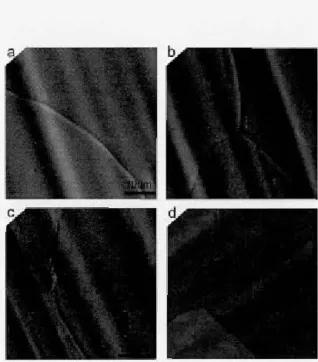
2.4 C1s XPS data for alcohol and methane grown graphene. Jo oxyge n-doped peak was observed for pristine graphen . . . . . . . . . . . 31 2.5 SEM images of graphene on 25llm Cu foi] substrates, compared
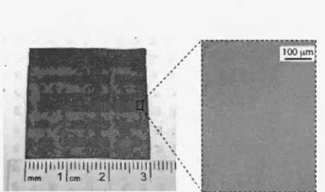
for growth by (a) methanol (b) ethanol (c) 1-propanol and (d) gas source rn thane. The images show the pre ence of Cu surface steps, and graphene wrinkles which result from the difference between the thermal expansion coefficient of graphene and Cu, indicating th at the graphene film is continuous and uniform. . . . . . . . . . 32 2.6 A 3 x 3 cm2 CVD graphene film grown using rn thanol, transf rred
to a Si02/Si substrate. . . . . . . . . . . . . . . . . . . . . . . 33 2. 7 Raman spectra of a tran ferred CVD graphene film on SiO 2/Si c
om-pared for growth by methanol, ethanol and 1-propanol. The small D p ak (1350 cm-1 ) and the inten ity of the 2D peak (2700 cm-1) found to be more than twic as high as the G peak (1580cm-1) indicate the presence of high quality monolayer graphene. 34 2.8 Raman spectra of tran ferred CVD graphene compared by pr
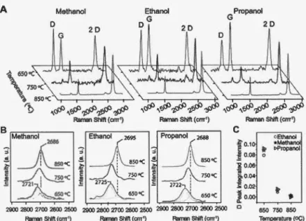
e-cursor and growth temperature. A Renishaw inVia spectrometer, 514.5mn laser wavelength, and 100x objective lens was used. (A) VVith a temperature increase from 650
o
c t
o 850o
c
,
the intensity of the D peak (1350 ClTI- 1) decreases and the 2D peak sharpens, ind i-cating a reduction in defect density and improved graphene quality. (B) Evolution of the D band with temperature, noting the fit of two Lorentzians ( 650o
c)
turning into one at 50o
c
,
characteristic of monolayer graphene. (C) Jo significant difference is observed in D peak integrated intensity versus alcohol precursor. . . . . . . . 35 3.1 XPS characterization of -doped graphene grown up to 30min-utes. Cls and N1s core-level X-ray photoelectron spectra of grown graphene from : a) ethylenediamine b) -methylimidazole. The C1s peak can be split to three Lorentzian peaks labeled by red, blue, and green lines corresponding to graphite-like sp2 C, J sp2 -C bond and CO (due to absorbed oxygen) re pectively. The N1s peak can be split to Lorentzian corresponding to pyridinic, pyrrolic and graphitic forms labeled by red, blue and green line respectively. . 40
3.2 XPS characterization of N-doped graphene grown up to 30 minutes from a) pyridine, and b) dimethyleformamide. The Cls peak can be split to three Lorentzian p aks labeled by red, blue, and green lines corresponding to graphite-like sp2 C, sp2 - C bond and CO (due to absorbed oxygen) re pectively. The Nls peak can be split to Lorentzian corresponding to pyridinic, pyrrolic and graphitic forms
lX
lab l d by red, blue and gre n lines respectively. . . . . . . . . 41 3.3 SEM image of a) the fast nucleation after 3 minutes of growth on
copper, the second and third layers are seen clearly over the first layer. b) Transferred film grown from eth y lenediamine after 30 min at 5 Torr of H2 press ur , large do mains of bilayer, trilay r and mul -tilayer over monolayer within several microns cover silicon dioxide. c) At 8 Torr of H2 a few domain of bilayer N-doped graphene are
een on transferred film on silicon dioxide. d) Monolayer ofN-doped graphene transferred on silicon dioxide using 10 Torr of hydrogen in the growth. . . . . . . . . . . . . . . . . . . . . . . . . 42 3.4 Raman spectra of monolayer N-doped graphene using precursors:
pyridine, dimethylformamide, N-methylimidazole and ethylenedi -amine. The measurements wer performed on films transferred on silicon dioxide. . . . . . . . . . . . . . . . . . . . . . . . . 44 4.1 Cls and Nls XPS spectra of copper amples af"ter CVD reaction
with nitromethane. . . . . . .. . . . 49 4.2 SEM image of a copper sample after having been exposed to a 15
minute CVD reaction with nitromethane. . . . . . . . . . . 50 4.3 SEM imag of a copper sample after having been exposed to a 30
minute CVD reaction with nitromethane. . . . . . . . . . . . 51 4.4 SEM image of a copper sample after having been exposed to a 45
minute CVD reaction with nitromethane. . . . . . . . . . . . 52 4.5 SEM image of a copper sample after having been exposed to a 60
minute CVD reaction with nitromethane. . . . . . . . . . . . 53 4.6 SE ~ image of a copper ample after having been exposed to a 75
minute CVD reaction with nitromethane. . . . . . . . . . . . . 54 4. 7 Average ho le diameter versus CVD growth time on copper sam
-ples using nitromethane as a precursor. Sample sizes of 10 (for 15 minutes) and 63 holes (30, 45, 60, 75 minutes). . . . . . . . . . . . 54
4.8 Mass loss statistics of 8 samples per reaction duration (15, 45, 60, 75 minutes), for nitromethane and methane ourced CVD reactions. For visualization convenience, mean error bars wer multiplied by a factor of 1000 for CH4, 100 for CH3N02 and the last data point
x
at 75
o
c
by a factor of 10. . . . . . . . . . . . . . . . . 55 4.9 Two Raman spectra aft ra 15 minutes nitrom thane-sourced CVDreaction on copper samples. . . . . . . . . . . . . . . . . . 56 4.10 Raw Raman sp ctral data on copper samples having passed through
a CVD growth using a) nitromethane and b) EDA/H20 mixture for a duration of 2 hours. Only the copper's Raman background is visible. . . . . . . . . . . . . . . . . . . . . . . . . . . . . . . . . . 56 4.11 Raman spectra on copper samples after standard CVD reactions
with methane, benzene, phenol, aniline, and nitrobenzene; formed under similar conditions as the methane growth .. A.l Cls XPS of benzene-sourced CVD sample.
A.2 Nls XPS of benzene-sourced CVD sample. A.3 01 XPS of benzene-sourced CVD sample. A.4 Cls XPS of aniline-sourced CVD sample. A.5 Nls XPS of aniline-sourced CVD sample. A.6 Ols XPS of aniline-sourced CVD sample. A. 7 Cls XPS of nitrobenzene-sourced CVD sample. A.8 N ls XPS of nitrobenzene-sourced CVD ·am pl . A.9 Ols XPS of nitrobenzene-sourced CVD . ample. A.lO Cls XPS of phenol-sourced CVD sample.
A.ll Ils XPS of phenol-sourced CVD sample. A.l2 01. XPS of phenol-sourced CVD sample. per-57 60 61 61 62 62 63 63 64 64 65 65 66
THE ROLE OF ITROGEN, OXYGEN, AND CARBON IN THE GROWTH
OF LARGE-AREA GRAPHENE MONOLAYER 0 COPPER CATALYST
Since its isolation in 2004 graphene persist ntly remains a ynthesis challenge. In order to take advantage of its full potential, high quality samples are requir d, i.e. large surfaces of mono-crystalline graphene. The Chemical Vapour Deposition
growth method is one of the synthesi methods capable of atisfying those needs. Moreover, graphene's chemical n-doping opens its application potential.
Using copper sheets as cataly t and several aliphatic precursors as carbon source, variable qualities of graphene can be produced. Methan and acetylene remain
the most popular precursors. In this work it is shown that graphene synthesis
from aliphatic alcohols (methanol, ethanol, 1-propanol) i possible, and that the presence of oxygen doesn't infiu -nee the quality of the final product. Moreover, doped graphene is achieved using precursor containing nitrogen a a heteroatoms; the resulting material is high-quality and poly-crystalline, with different doping percentages.
Finally, using a selected series of precursors, it is shown that the simultaneous
presence of carbon, oxygen, and nitrogen behaves antagonistically to graphene's growth. The catalyst's surface changes its topography and the spontaneous growth
of the material is inhibited.
RÉS MÉ
LE RÔLE DE L'AZOTE, OXYGÈNE, ET CARBO TE DA TS LA CROISSANCE D'UNE L RGE !IONO-COUCHE DE GR PHÈ TE SUR LE
CATALYSEUR CUIVRE
Depuis son isolation en 2004 le graphène reste toujours un défi de synthèse pour
les scientifiques. Afin de profit r du potentiel du graphène, cl s échantillons de haute qualité ont dé irés, i.e. larg · urfaces de graph 'ne mono-crystallin. La synthè e par dépôt chimique en phase vapeur ( CVD) est une de méthode de syn -thèse capable de satisfaire c s b oin . De plus, le dopage n de c matériau ouvre sa gamme d'application ..
En utilisant des feuilles de cuivre comme catalyseur t cliff' rents pr' curseur aliphatiques comme ource de carbone, variables qualités de graph 'ne peuvent être produites. Le méthane et l'acétylène r stent les précurseurs les plus pop -ulaire. . Dans ce travail il t montré que la synthèse à partir cl 'alcool alipha -tique· (méthanol, éthanol, 1-propanol) st po sible, t en ·ore, que la pré ·ence de
l'oxygène n'influence pas ur la qualité elu matériau final. D plus, la modification du graphène par dopage est achev' e en utili a.nt des précurs urs cont nant l'azote comme hétéroatome; le ré ultat est du graphène de haute qualité, poly-crystallin, à différents pourcentages de dopage.
Enfin, en utilisant de précurseurs spécifiques il est montré que la présence simul -tanée du carbon , oxygène, et azote réagit de manière antagoniste à la croissance du graphène. La surface du catalyseur change de topographie t la croi . ance spontanée du matériau est inhib 'e.
LIST OF ABBREVIATIONS, SYMBOLS, AND ACRO YMS 2D 3D Â AFM Au
c
CNT C02 CH4 CH3N02 Co Cr Cu CuO Cu20 CVD DMF DNA EDA ESCA H2 H20 Ir F FeC13 F\NH!VI Two dimensional Three dimensional Angstrom Atomic Force Microscope Gold Carbon Carbon Tanotub Carbon dioxide Methane Titromethane Cobalt Chrome Copper Cupric oxide, or copper(II) oxide Cuprous oxide, or copper(I) oxide Chemical Vapor Deposition Dimethy lformamidDeoxyribonucleic acid Eth y lenediamine Electron Spectro copy for Chemical Analysis Hydrogen \iV a ter Iridium Fluorine
Ferric chloride, or iron(III) chloride Full-width at half-maximum
XlV
GaAs Gallium Arsenide
M M tal Ii Iickel 2 Nitrogen 02 Di-oxygen Pd Palladium PDMS Polydimethylsiloxane
PMMA Polymethyl methacrylate
ppb Parts per billion
Pt Platinum
Re Rhenium
Ru Ruthenium
SE 1 Scanning Electron !Iicroscopy
Si Silicon
SiC Silicon Carbide Si02 Silicon Dioxide
sp2 Trigonal atomic orbital hybridization
sp3 Tetrahedral atomic orbital hybridization T Temperature in
o o
c
TEM Transmission Electron Microscopy UV Ultra-Violet
XPS X-Ray Photoelectron Microscopy
Zn 0 Zinc Oxide
0.1 Carbon Allotropes and Nanocarbons
Over 95% of our surrounding chemical environment is composed of "carbon
com-pounds". Organic chemistry forms the backbone of life. Among other elements which manage to bond with themselves in long chains, carbon is among the most
versatile and strong. It can form single (bond energy of 350 kJ mol-1), double (610kJmol-1), and triple bonds (840kJmol-1
) with itself leading to a variety
of structures and conformations useful in many fields of research. (Wu dl, 2007)
Historically, diamond and graphite were considered the main allotropie forms of carbon. Now, among them there are around a dozen forms. Amorphous carbon, obtained as a product of combustion from sorne materials, is composed of various
ratios of sp2 / sp3 hybridized car bons in no particular crystal arrangement. Other notable allotropes are fullerenes, nanotubes, carbynes, and the recently popular
graphene.
Diamond is the hardest material known, with a hardness of 10 on the Mohs scale, and it's the thermodynamically stable form of carbon above 60 kbar of pressure. Its sought-after properties as well as its as-close-to-perfect-as-possible crystal structure receive numerous applications in science. It is a patent abra -sive material, and it can be industrially synthesized. Diamond is composed of only sp3 hybridized carbons, in which each carbon is covalently bonded to four
other car bons. In conditions such as low pressures and under 1500
o
o
c
diamond thermodynamically transforms into graphite. This conversion is very negligible in2
ambient conditions. (Wu dl, 2007)
Graphite can be pictured as a stacking of an infinite number of layers of sp2
-hybridized carbon atoms; this layer is known as a graphene sheet. In such a
layer each carbon atom is bonded to three others. This arrangement resembles
the honeycombs of bees, a planar matrix of bonded hexagons. Each carbon has
one unhybridized electron in the 2pz orbital. The association of all these elec
-trons forms delocalized n orbitais, assuring further stabilization for the in-plane
bonds, much like scaffolds on both sides of a wall. Each layer has these deloca l-ized orbitais on both sides, meaning that the stacking of the layers is based on
n- n interactions of Van der Waals nature. The layers are stacked together about
3.35 Â.(Chung, 2002)
The most common form of graphite stacking is the hexagonal ABAB; a less often
version being the rhombohedral ABCABC. The various stacking arrangements and the weak Van der Waals interactions contribute to graphite's lubricant pro
p-erties. Moreover, its electronic configuration gives it good planar (following the n
bands and the Πbonds) conductive properties, of both electricity and heat; less so
in the stacking direction due to Van der Waals interactions. An "imperfect" version is the turbostratic graphite, in which the inter-layer distance is variable due to a
multitude of stacking faults (layer rotations or translations). Artificially, one can prepare well-ordered pyrolytic graphite through pyrolysis of a gas carbon source. Annealing this form of graphite produces highly oriented pyrolytic graphite with
a mosaic spread of 0.02° and crystallites of around lpm in size.(Wudl, 2007)
and nanotubes have been discovered and studied since the mid 1900's. Both ma -terials form when the dangling bonds at the edges of a finite graphene layer bond together. The end product depends on the nature of the topological manipula -tions happening with graphene. The result has a lower material energy, but with increased bond strain. (Wu dl, 2007)
Fullerenes are hollow spheres formed of various numbers of carbon atoms depe nd-ing on shape and size, the most popular being C60 and C70 . The bond strain allows for facile functionalization opportunities of fullerenes. This has allowed scientists to take advantage of their properties in various fields, such as solar cells, and biologie al applications. (Wu dl, 2007)
Carbon nanotubes also have their own merit due to their electric and mechanical properties. Depending on the folding axis of the graphene sheet, the resulting na n-otube can behave either as a metal or a semi-conductor. Chemical functionaliza -tion is also relatively easy, allowing for applications in nanoelectronics, reinforcers in composite materials, biosensing, tissue engineering, drug delivery.(Wudl, 2007) Carbon onions are spherical concentric shells of graphene, or multi-walled fullerenes. One immediate application studied was the encapsulation of other materials for protective purposes. (Wu dl, 2007)
Amorphous carbons have a longer history than their more exotic counterparts. They consist of roughly planar layers of sp2-hybridized carbons, with varying fractions of sp3 carbons which provide crosslinking between neighbouring layers. These materials lack a well-defined crystallinity. These "soft carbons" can be prepared from the gas phase. on-graphitizable carbons originate from solid pre -cursors (polymers, resins) and have a high degree of disorder. They have isotropie properties, and their high degree of cross-linking do not allow for the formation
4
of graphitic structures. Activated carbons are part of the amorphous allotropes
which have undergone chemical modifications. They are usually porous, with high
surface are as ( 500 m 2 g-1 to 3000 m 2 g-1
). (Wu dl, 2007)
0.2 Applications and Perspectives
The energy sector seems to be the most popular field in which carbon materials
are used. Due to the versatility of its electronic structure through hybridization,
carbon can form various structures. A series of processing routes allow scientists
to take advantage of its versatility, obtaining modified versions, such as carbon
fibers, carbon foams, mesa-carbon-micro beads, and even carbon-carbon compos
-ites.(Srivastava et al., 2009)
Graphite, the most common allotrope, has been used as a writing tool for hundreds
of years. Its powder form has also proved to be a good dry lubricant, although
that is due to the air trapped between the graphene layers. In vacuum the layers
are subjected to Van der Waals interactions which make their separation quite
diffi.cult. (Wu dl, 2007)
The delocalized 1r electrons in the graphene layers are responsible for graphite's
in-plane conductivity. (Wu dl, 2007) A mixture of carbon black (able to hold elec
-trolytes) and graphite (conductive) is used in non-rechargeable batteries, and
various carbon designs are used in rechargeable batteries: carbon fibers, carbon
micro-beads, pitch coke, polymer-based carbons.(Srivastava et al., 2009)
Sorne forms of carbon are known for their high H2 absorbing capability. This has been exploited for applications in fuel cell technologies for parts such as catalyst
supports, gas-diffusion systems, current-collector plates. Catalyst-filled carbon
nano-tubes can be used as a membrane in fuel cells where they proved to be very
effective in the reduction of oxygen and oxidation of methanol. (Srivastava et al.,
Hydrogen storage is another very attractive research subject. Its combustion pro-duces energy and water vapours, with an energy density of 38kWhkg-I, almost 3 times that of gasoline. The cavities and micro-pores of carbon materials make them interesting candidates for hydrogen storage. However, it has been shown that C T-derived materials have the highest potential due to their large external
surface and the variable internai hollow cavity where gas can be stored by phys i-or chemi-sorption. (Srivastava et al., 2009)
According to the study of Chesnokov et. al CNTs present a spring-like behaviour under 25kbar of pressure.(Chesnokov et al., 1999) This makes them promising candidates in composites for energy absorbing materials.(Srivastava et al., 2009)
As far as electronic applications go, carbon allotropes have a rich potential. CNTs behave either as a metal or semi-conductor depending on their chirality - useful in flat panel displays, computer chips, cell phones, nano-circuitry.(Zhang et al., 2007) Fullerenes seem useful in electronic textiles, molecular transistors, solar pa n-els, and even electromagnetic interference shielding. (Srivastava et al., 2009)
0.3 Conclusion
Carbon is a highly versatile element present everywhere around us, from it being the support of life to forming the hardest and strongest materials known to man. Its present and under-study applications cover a wide spectrum of fields which show considerable promise to improving human life.
CHAPTER I
CHARACTERIZATION METHODS
In this chapter a series of characterization techniques are presented. They are
practical applications of matter-matter and energy-matter interactions
phenom-ena.
1.1 Atomic Force Microscopy
Atomic Force Microscopy (AFM) was initially presented as an application of the
"tunnelling effect" concept, allowing the surface study of electrically insulating
materials. Combining tunnel effect microscopy and a profilometry stylus, Bin-nig, Quate, and Gerber showed that it is possible to get images of surfaces in ambient air, whether the material is conductive or not, with a resolution of 30 Â
vertical, and 1 Â horizontal. (Qua te, 1986) It has sin ce been adapted to different
environments: liquid, low temperatures, magnetic fields, and even optimized for
biological and chemical applications.
The working principle is based on the measurement of the forces between the
stylus and the analysed surface. The force is measured by a cantilever. Surface interactions modify the cantilever's shape, these are observed by following the
refiection of a laser bearn off its tip.
1.1.1 Microscope
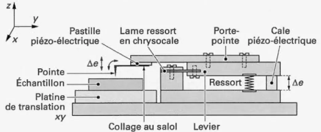
A miniature tip on a cantilever approaches the sample surface. The sample is kept on a xy translation stage which moves it relative to the tip (Figure 1.1). An AFM tip can work in static or oscillating modes.(Frétigny, 2005)
Collage au salol Levier
Figure 1.1: AFM cantilever and tip assembly schematic.(Frétigny, 2005)
There are three main operating modes on an AFM: static, dynamic, and thermal.
The interactions can come from the Van der Waals forces between the tip and the sample, capillary forces, friction, and even magnetic processes. Chemically modifying the tip gives the opportunity to consult various surface properties of the sample.
Using a control loop it is possible to obtain "height, information of the surface (topography) by following a constant mechanical interaction; moreover, it also per -mits the measurement of viscoelasticity, tribological, and friction measurements. Another possibility is the measurement of distant forces between the surface and
8
the ti p. (Frétigny, 2005)
1.1. 2 Opera ting modes
Without vibrating the cantilever, the sample is brought doser to it (z axis) and the cantilever defiection is measured. One cycle is enough to obtain a force curve describing the sample-tip interaction. On approach, the interactions are weak,
there is little to no defiection of the cantilever. In vacuum, air, liquids, this interaction is slightly attractive, phenomenon described by a negative cantilever defiection. Closing in even more, the defiection grows linearly with sample height. During retraction, the force curve carries the same shape as on approach, but surpasses the null force point; the adhesion forces are keeping the cantilever close to the surface. Once enough force is applied to release the tip the force curve resumes the same behaviour as on approach. This is resumed in Figure 1.2.
~ 3 :::J Q) ( )
0
2 u.. 0 - 1 - 2 - 3 0 Contact : ' ' ' ' ' ' ' ' ' 'l
'v
' ' ' ' ' ' ' ' ' ' ' Tapping ' ' ' 1 1 2 Résonnant ...-; : ' ' ' ' ' ' ' ' ' ' ' '/'"
1--'" ' ' ' ' ' ' ' ' ' ' ' 4 6 8 10 zéch (u.a.) Figure 1.2: Surface-tip interaction curve. (Frétigny, 2005)Contact mode
Following the force curve acquisition it is easy to continue into contact imaging mode; the defiection force of the probe is maintained constant, as the sample is translated on the x,y,z axis. The probe is in constant contact with the surface. This can, however, damage the surface of the sample, and reduce image quality. Tonetheless, it is a quick and easy method of imagery. It is often coupled with measurement of friction and adhesion forces, as well as contact stiffness (Young modulus).(Frétigny, 2005)
Resonance mode
The resonant mode uses the cantilever's natural resonance frequency. Far from the sample, and with a low amplitude, the cantilever oscillates. The force gradient depends on the tip position on the surface, and it causes a frequency displacement in the cantilever. Inversely, at a given oscillation frequency, the amplitude is mod-ified and gives information on the local force gradient. This mode is seldom used in topography imagery, however it is useful in measuring long distance, electrical, and magnetic interactions.
Tapping mode
It is a non-linear resonance mode which consists of higher amplitudes and a shorter tip-sample distance than the resonance mode. With each cycle the tip gently "touches" the surface at a frequency close to the cantilever's resonance. The ap-plied forces on the sample are significantly weak and the contact time is short, thus this mode is ideal for topographical imagery as the friction produced is in-significant. The sample is maintained intact, with little to no deformation or wear.
10
Moreover, the short contact time limits surface adhesion.
1.1.3 Other analysis
The AFM tips can be functionalized in order to study different materials' prop-erties such as adhesion, chemical functionalization and specifie chemical interac-tions, polymer elasticity. Generally, carbon nanotubes are used which provide a few-nanometers diameter tip useful for analysis.(Frétigny, 2005)
AFM is a highly versatile force measuring tool, capable of contact and distant forces measurement applicable in materials science, cellular biology, interface and surface studies, as well as indirect analysis through these methods.
1.2 X-Ray Photoelectron Spectroscopy
Atoms present at the surfaces of materials are the first responders to any inter-action attempt with the bulk. The nature of these atoms dictates the types of interactions taking place: corrosion catalysis, contact potential, adhesion. T here-fore, surfaces influence a number of properties of the bulk. However, only a small number of these atoms are actually found on the surfaces. If we consider a 1 cm3
cube, only an estimated 1 in 107 are present on a surface, giving roughly a con-centration of 100 ppb. Obviously, this ratio depends on the morphology of the studied surfaces. In order to successfully analyse a surface, the technique used must be highly sensitive, and capable of filtering other interfering signals coming from impurities. One of the techniques used capable of satisfying surface analysis is X-ray Photoelectron Spectroscopy. This technique is effective at identifying surface elements, describing and quantifying their chemical states, giving a 3D distribution of elements, and even identifying if the surface is populated by thin
films.(Wolstenholme, 2003)
1.2.1 Electronic Spectroscopy
Electron spectroscopy is interested in the emission and analysis of low-energy electrons, usually 20 eV to 2000 eV. These electrons are emi tted by the materials as a result of the photoelectric effect; Einstein's mathematical description of this
phenomenon earned him a obel prize in Physics in 1921. Those electrons have a kinetic energy as such:
KE
=
hJ-t - BE- <I>s (1.1)where hJ-t is the photon's energy, BE the binding energy of the originating atomic orbital, and <I>s is the spectrometer's work function. (Moulder et al. 1992) These photoelectrons can be emitted from different shells, each at a specifie energy and with different emission probabilities.
Electron-matter interaction happens more often than photon-matter, thus the
electron mean free pa th is considerably sm aller ( tens of Angstroms) th an pho-tons' ( micrometers). This means th at the only electrons capable of leaving the
bulk without energy loss are those present at depths inferior to tens of Angstroms. These electrons give the useful signais. The background is formed by electrons which have gone through energy loss processes. Useful electrons are then detected by an electron spectrometer according to kinetic energy.(Moulder et al., 1992)
1.2.2 Interpretation
A general XPS spectra is a plot of electron binding energy versus the number
12
from the electrons which haven't lost any energy while being ejected from the
sample. The electrons are randomly collected in time, as a consequence the sig
-nais appear with sorne "noise" which isn't instrumental. The percent standard
deviation for counts is indirectly proportional to the square root of the number of counts; the signal-to-noise ratio is proportional to the square root of the counting time.(Moulder et al., 1992)
1.2.3 Identifying the chemical state
Properly characterizing a material by XPS first requires a good line identification.
This can be made easier with proper instrumentation (voltage calibration, narrow
sweep range). An immediate challenge is the static charge accumulation which needs correction. Insulating samples may acquire a steady-state charge during
analysis. Positive charging is capable of shifting peaks to higher binding energies, while the opposite is applicable to negative charges. In order to overcome this obstacle there are a few steps which can be taken. The C1s position can be
mea-sured, known to appear at 284.6eV; any shift from this value can be considered as a measure of the static charge. Trace quantities of Au can be evaporated on the
sample; the Au4f doublet is recorded, then the analysis of interest is repeated. It is assumed that the potential of the gold islands refiects the surface charge of the
sample. A simple correction can also be made with an internai standard. (Moulder
et al., 1992)
There are numerous factors concerning the proper interpretation of XPS chemical
shifts, which is why peak assignment and data comparison is still done through cross referencing with literature.
Case of Carbon nanomaterials
The surface analysis potential of XPS is particularly useful in carbon materials studies due to the importance of surface structure and chemical composition which dictate the material's properties.
XPS spectra are able to provide information concerning the degree and nature of functionalization. Carbon nanomaterials have a highly versatile surface from a chemical point of view, supporting a large number of reactions. It is then impo
r-tant to clearly determine the chemical states of the elements at the surface. It is also known that C has several hybridization states, each with different character
-istics which influence the material's behaviour. Graphite for instance is composed
of mostly sp2bonded carbons (sp3 being present at the edges). An XPS spectrum of this material should theoretically give a single peak of Cls around a binding energy of 284.2 eV. On the other hand diamond materials have a fully sp3 bonding
construction. The XPS signal of these materials should give a single peak around 286 eV. Following this information it is then easy to determine a ratio between
the two kinds of hybridization by comparing the respective peaks. For instance the laser treatments of graphite produces diamond-like domains in the material. Higher the laser intensity, higher the sp3 content.(Barron, 2011) Such an example can be seen in Figure 1.3.
In general, binding energy increases with decreasing electron density around the atom. Positive oxidation states register higher binding energies, in contrast with the reduced species which gain shielding, easing the electron expulsion.
As it was shown, XPS is a versatile technique in identifying the elemental compo
-sition of a material, as well as their the relative ratios. Furthermore, information
C1s
Diamond Orapl1i1e -84 286 288 _90 Binding energy (eV) Laser Power 14Figure 1.3: C1s high resolution XPS spectra of graphite, nanodiamond, and graphite with increasing laser power treatment. Adapted from Mérel et al. 1998.
This is a confident starting point in determining the carbon materials' properties, notably at the first atomic layers which are the most active.
1.3 Scanning Electron Microscopy and Transmission Electron Microscopy
In the early 20th century the electron's wave-particle duality was discovered. At a 50 V acceleration their wavelength reaches 0.17 nm. Such dimensions are com-parable to atomic dimensions, making electrons useful in characterizing materials as they are strongly diffracted from th array of atoms on crystals' surface. At a 1000 times stronger acceleration (50 k V) their wavelength re aches 5 pm. These conditions allow a material penetration of up to several pm. In case of a crys-talline solid the electrons are diffracted by the atomic planes. This is at the basis of transmission lectron diffraction. Later, it was discovered that if these elec-trons could be focused the images obtained would have better spatial resolution than ligh-optical microscopes. Focusing electrons requires magnetic fields given
the particles' negative charge.(Egerton, 2005)
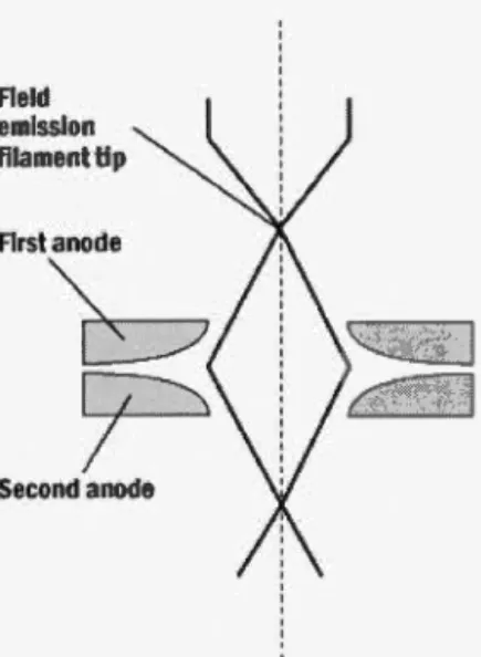
Aeld emission filament tlp
15
Figure 1.4: Electron bearn source. Illustrated, a field emission filament tip cathode and the anodes responsible for the electron extraction. (of Iowa, )
1.3.1 Scanning Electron Microscopy
In SEM electrons are both elastically and non-elastically scattered when ente
r-ing a solid. Sorne of them are elastically scattered at angles >90° with enough energy to leave the specimen and enter the vacuum - they are then collected as backscattered-electrons (BSE) and processed into a signal. Inelastic scattering
involves low defiection angles, but it may reduce kinetic energy of the incident electrons until they are absorbed by the solid, and possibly become conduction electrons (in case of metals). The penetration depth increases with increasing acceleration energy. (Egerton, 2005)
1.3.2 Secondary Electron Imaging
Weakly bound electrons (mainly found in the outer shells) use only a small portion of the incident energy as means of escape from the atom's shell. The remaining energy is then kept as kinetic energy. These secondary electrons will eventually
16 non-elastically interfere with matter even before they escape the bulk. In doing so they lose kinetic energy, and only the ones originating near the surface are able to escape and be detected. The escape depth is generally <2 nm, thus images formed by secondary electrons (SEI) present a topographical contrast. There is almost always a contrast due to the fact that the secondary electron detector is
positioned on the side of the column at an angle. The images are comparable to observing an abject lighted on one side- brighter on the side more exposed to the
light source. In the case of SEM the bright features are those facing the detector
as the electrons originating from those zones have a higher probability of reaching
the detector. (Egerton, 2005)
1.3.3 Backscattered Electron Imaging
Backscattered electrons are primary electrons scattered at angles >90° from the solid. Seeing how this interaction is elastic the energy of these electrons is similar
to their initial acceleration. The backscattering coefficient depends strongly on
the atomic number of the matter's composition. This gives elemental contrast images (Z dependant). (Egerton, 2005)
1.4 Raman
One of the most versatile and pertinent spectroscopy method used in this project
is Raman spectroscopy, which has molecular vibrations as focus. The sample is excited by a laser at a set wavelength, and the scattered photons are recorded and analysed. The data extracted from them is capable of describing the vibrational
state of the analyte.(Dent, 2005)
There are 3 sort of light scattering modes: Rayleigh diffusion which is simply the incident light elastically refl.ected at the same frequency as the incident light,
Stokes scattering which is diffused at a frequency lower than the incident light's (it subtracts the molecular vibration frequency), and anti-Stokes scattering at a higher frequency (it adds the molecular vibration frequency); these latter two compose Raman spectroscopy. Stokes lines are the most studied as their intensity is higher than anti-Stokes'.(Palsson, 2003)
1.4.1 Raman Fingerprint of sorne Carbon allotropes
Carbon is most abundantly present under its graphite form, among diamond, graphene, nanotubes, and fullerenes. The main allotropes studied are graphene and graphite.
Graphene
It is a 2D material, fully composed of sp2 hybridized carbons. Its crystal lattice has a hexagonal symmetry (D6h), and its crystal structure has 2 atoms per lattice. For 2D structures Raman spectroscopy can give information on crystallite size, hybridization, presence of impurities, mass density, band gap energy, doping, de -fects and other crystalline disorders, number of graphene layers, carbon nanotube diameter, and even metallic versus semi-cond uctive behaviour. (Ferrari, 2007)
There are three main Raman bands for pristine graphene, G (1582 cm-1 ), 2D (2500cm-1 to 2800cm-1
), and D (1345cm-1). The G peak originates from the
elongation of the C-C bonds common to all the sp2 hybridized systems. These bonds characteristics can be infiuenced (deformations, interactions with substrates or other interfaces) which in turn modify the hexagonal symmetry. For instance nanotubes' curves give a more complex G peak signal, while pristine graphene gives a single clear peak. (Ferrari et al., 2006)
18 (a) 514 nm 50000 40000 Graphite :::::1 cu ___.. >. 30000 ...
ën
c Q) 1)l
... 20000 c 10000 Graphene 0 ~\ A 1500 2000 2500 3000 Figure 1.5: Comparison of Raman spectra at 514 nm for bulk graphite and graphene; scaled to illustrate a similar height of the 2D peak around2700cm-1.(Ferrari et al., 2006)
The 2D band is a consequence from a phonon-phonon interaction, and it's dis
-persive, meaning the response signal depends on the excitation wavelength. This
band can give information concerning graphene's electronic structure as well as
its phonons, i.e. it is possible to differentiate mono, double, and several layered
graphene, as well as its electronic structure. Practically, the 2D band has specifie deconvolutions for graphene of 1 to 5 layers, above which the material's electronic structure begins to resemble graphite's and adopts that electronic and vibrational
definition. (Ferrari et al., 2006)
The last band of interest is the D band, known to appear from disorder in the
sp2 hybridized systems. These defects induce interesting resonance phenomenons. For instance it is possible to quantify the disorder in systems by comparing the 2D to G intensity ratios. Moreover if the ratio is lower than 0.5, then a single layer
of graphene is present, a ratio of 1 means that there are 2 layer, etc., however this quantification becomes difficult with increasing number of layers, as the effect on
the intensity isn't linear. Another piece of information stems from doping induced
resonance. Whenever a system is doped a D' peak appears which is an overtone
band of the D band. Finally, several smaller peaks are present in a pristine
graphene spectrum, however they are sim ply overtones. (Ferrari et al., 2006)
Graphite
Figure 1.6: The crystal structure of graphite. Illustrated, its primitive unit cell,
with dimensions a= 2.46 Â and c
=
6.71 Â, and an in-plane bond length of 1.42 Â.A, A', B, and B' are the four atoms forming graphite's unit cell. Atoms A and A'
(full circles) have neighbours directly above and below in adjacent layer planes;
B and B' (open circles) have neighbours directly ab ove and below in layer planes
6.71 Â away.(Chung, 2002)
Graphite is simply put stacked graphene in an AB sequence. Its unit cell is com-posed of 4 atoms. This material has numerous vibrational modes, however only
two are Raman active: the modes E2g1 and E2g2. E292 is observed at around
1582 cm-I, close to benzene's C-C vibration frequency. The second order har
-monies of this mode is recorded at 3248 cm-1
. Less information is available for
the E2g1 mode, although it has been measured to appear around 42 cm
-1
.
Infe-rior quality graphite presents a Raman peak at around 1355 cm-1 assignable to
20
There are a few differences between graphite and graphene, as far as Raman spectroscopy goes. The 2D peak can be split in two elements for graphite: 2D1
and 2D2 with heights about 1/4 and 1/2 of the G peak respectively. It is also known that graphene's electronic structure evolves with increasing the number of layers. The 2D band has a single component for monolayer graphene, and reaches two components for the graphite. (Chung, 2002)
1.5 Conclusion
AFM, XPS, SEM, TEM, and Raman were covered, shown as versatile and co m-plementary characterization techniques. All of them have been used during the study presented here.
GRAPHENE GROWTH FROM METHANE A D ALIPHATIC ALCOHOLS
2.1 Graphene, introduction
Since its isolation in 2004 by the Novoselov team the 2D material known as graphene has been the focus of several multi-disciplinary research subjects. Graphene
is a material composed of sp2 hybridized carbon atoms in a honeycomb lattice
with a mono-atomic thickness estimated at around 8 Â. (Dimitrakopoulos, 2012)
It has been found that this material possesses various exceptional properties which
stimulate the researcher's efforts in a large number of fields. Its crystal structure grants a particularly interesting band composition. Individual carbon atoms are separated by about 1.42 Â from their 3 neighbours, constituting aromatic bonds in resonance. (Gray et al., 2009) This gives rise to a zero band gap material acting as a semi-metal. As a consequence the charge carriers passing through it behave as
Dirac fermions (zero effective mass), allowing them to ballistically travel up to 1 micron with mobilities of around 200 000 cm2
v
-
1 s-1, a half-integer quantum Halleffect, all this while absorbing merely 2.3% of visible light. (Lee, 2013) Among the
most sought after applications are high frequency electronic deviees, and trans -parent conductors. Its "miracle" characteristics have been observed while studying
high quality samples, notably from mechanical exfoliation, and from its depos
i-tion on boron nitride. The alternative synthesis methods have yet to achieve these
22
2.2 Graphene synthesis methods
There are numerous methods of graphene and graphene-like structures production with various sizes, shapes, and quality, however only a few are industrially scal-able. Among those we note liquid phase and thermal exfoliation, epitaxial growth on SiC, and Chemical Vapour Deposition.
2.2.1 Exfoliation
The exfoliation methods depart from graphite with the goal of separating the individual graphene flakes which compose it. The liquid method has two main paths, the first uses non-aqueous solvents with enough surface tension to favour an increase in the total area of the graphite crystallites, the second focuses on aqueous solutions of surfactants. Sonication, plus further treatment, aids the split of suspended monolayer flakes of graphene. A related route is the graphene oxide formation by oxidizing graphite crystallites, ultrasonically exfoliated, then processed. These methods allow the deposition of the material on almost any surface. Industrially it is more efficient to use a thermal shock procedure fol-lowing the graphite's oxidation, which simultaneously achieves reduction and ex-foliation. (Novoselov et al., 2012) Moreover, it is possible to obtain graphene nanoribbons suspensions by carbon nanotube unzipping. These are more expen-sive methods, but can assure a tonne-level of production of well-defined distri-butions of graphene. Research is under way to use these methods in creating graphene-based inks, paints, electronics, electromagnetic shielding, barrier coat-ings etc.(Novoselov et al., 2012)
2.2.2 SiC epitaxy
It has been demonstrated that graphitic layers can be grown on both faces of a SiC wafer by sublimating Si atoms leaving behind graphitized carbon. This method
yields very high quality graphene with domains capable of reaching hundreds of microns in size. Despite its attraction this method has several drawbacks. SiC
wafers are costly, and the temperatures required for the sublimation go beyond 1000 °C. Moreover, the SiC surface's required homogeneity is high - dangling
bonds, if present, are able to bind covalently with graphene, thus rendering the
first layer unusable.(Riedl et al., 2010) onetheless, SiC graph ne has sorne niche applications such as high frequency transistors, short-gate transistors, and even in metrological resistance standards. ( ovoselov et al., 2012)
It is apparent that the high temperature issue remains the most important. More -over, future work should address the other problems such as elimination of te r-races, the growth of multi-layer graphene at the edge of terraces, unintentional doping from the substrate and buffer layers, as well as increasing the crystallites size.(Novoselov et al., 2012)
2.3 Chemical Vapour Deposition graphene growth
Chemical vapour deposition (CVD) is one of the methods capable of producing
24
2.3.1 Chemical Vapour Deposition systems
As its name implies, the CVD system involves the use of vapours from various
sources, either gas, liquid (evaporation), or solid (sublimation). The vapour flow
is generally measured by mass-flow controllers. Vapours are then passed through high-temperature resistant tubes of quartz, ceramic, or stainless steel. The vapour
circulation is assured by a vacuum system, and the pressure measured by thermo
-couple and ion gauges for higher vacuum. The vacuum, depending on the use, is
provided by a simple mechanical pump, or by more powerful combinations of
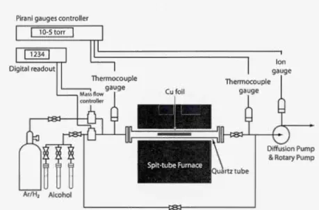
dif-fusion with mechanical pumps, as in our case (Figure 2.1), or by a turbo-molecular pump.
Pirani gauges controller 10-5 torr
Spit-tube Furnace
Figure 2.1: Schematic representation of the used CVD system. ( Guermoune et al.,
2011).
2.3.2 CVD graphene growth process
The formation of few layer graphene on transition metal surfaces (Re, (Miniussi
Co,(Ago et al. 2010) i,(Kim et al. 2009) Pt,(Sutter et al., 2009) Pd(Kwon
et al., 2009)) has been demonstrated in the past few years. The deposition mec h-anism depends on the growth conditions and carbon solubility. Results of growth on inexpensive polycrystalline i and Cu substrates have stimulated the interest in using CVD for large area depositions. Copper proves to be the most efficient catalyst as far as priee, handling, and quality of graphene go. Over 95% of the copper surface is covered by single layer graphene, the rest being multilayer. (Li
et al., 2009a) Graphene growth on copper involves the thermal decomposition of
a carbon source at high temperature. Gas, liquid, and solid precursors such as
acetylene,(Nandamuri et al., 2010) methane,(Li et al., 2009a) hexane,(Mendoza,
2011) alcohols,(Guermoune et al., 2011) and polymers(Byun et al., 2011) can be used. Another important factor is the catalyst pre-treatment. As-received
copper substrates are covered by native oxides (CuO, Cu20) which may diminish
copper's catalytic activity. Two steps have been proven to remove these oxides.
First a wet chemical pre-treatment by dipping in acetic acid, then an annealing
treatment at 1000 °C. Besides oxide removal, the annealing increases the Cu grain
size and modifies its morphology, which has been shown to have an effect on the
size and quality of the graphene domains.(Han et al., 2011)
The growth mechanism starts from nucleation sites from which flakes of graphene
grow. With time the graphene domains increase in size, and eventually coalesce
into one continuous layer. It has been shown that by tuning the pre-treatment
conditions, partial pressure of the carbon source, and total growth pressure the
nucleation density and flake size can be controlled. After the growth of a c ontinu-ous sheet of graphene further exposure to the growth conditions does not lead to
the formation of multiple layers of graphene. It has, however, been shown that the
26
graphene.(Cui et al., 2012)
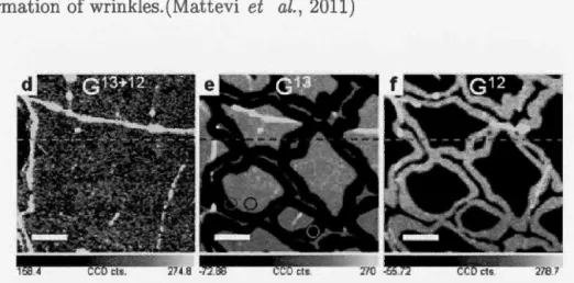
The growth mechanism is a surface phenomenon, and not related to diffusion
from bulk. This has been illustrated by the Ruoff group while growing graphene
with a sequence of 13CH
4 and
12CH
4 (Figure 2.2). The Raman signatures of
the two carbons differ slightly, which in turn translates into well differentiated
Raman maps illustrating the regions in which 12C and 13C were sequentially used
as precursors. (Li et al., 2009b)
The as-grown layer of graphene contains wrinkles, explainable by the difference
in the thermal expansion coefficients of the catalyst and graphene ( O'.graphene
=
-6 x 10⁻⁶ K-1 at 27 °C, O'.graphite = 0.9 x 10⁻⁶ K-1 between 600
o
c
to 800 °C,a.cu
=
24 x 10-6 K-1). These values suggest that graphene shrinks significantly
with Cu cooling, generating mechanical stress, and its release is translated into
the formation of wrinkles. (Mattevi et al., 2011)
Figure 2.2: Micro-Raman characterization of the isotope-labeled graphene grown
on Cu foil and transferred onto a Si02/Si wafer. Integrated intensity Raman maps
of (d) G13+12 (1500cm-1 to 1620cm-1), (e) G13 (1500cm-1 to 1560cm-1), and
(f) G12 (1560cm-1 to 1620cm-1). Scale bars are 5pm.(Li et al., 2009b)
measuring its carrier mobility, optical transparency, and sheet conductance.(Cooper et al., 2012) In order to perform those measurements the film must be transferred onto other substrates. This is usually done by first depositing a polymer coating on the graphene film, typically PDMS or PMMA, then etching the underlying copper in a FeC13 or (NI-14)28208 (ammonium persulfate) solution. This last step is performed by immersing the graphene bearing substrate on the etching bath un
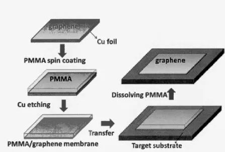
-till a free-standing polymer/graphene membrane is observed fioating on the bath. The transfer step has been proven to cause damage to the graphene film. (Kang et al., 2012) In order to minimize the film cracking it is important to promote a high adhesion between graphene and the target substrate. Roughness and hy -drophobicity are the main factors infiuencing graphene's adhesion. (Martins et al., 2013)
The transfer procedure exposes the graphene to various chemicals and to certain degrees of mechanical stress. These factors participate in producing or enhancing structural defects in graphene,(Kang et al., 2012) as well as possibly introducing undesirable impurities.
~rapheneA
...a.··
.··
Cu f01lPMMA spin coating
Dissolving PMMAt
Transfer PMMA/graphene membrane
Figure 2.3: Schematic representation of the transfer procedure of graphene grown on copper foils.(Lee, 2013)
28
So far its properties have been maintained at a satisfactory level. Reported mobil-ities vary between 700 cm2
v-
1 s-1 to 3000 cm2v-
1 s-1. The best optoelectronic properties have so far been obtained by Bae et al. 2010 with a Hall mobility of 5100 cm2v
-
1 s-1 and a sheet resistance of 30 D at 90% transmittance. (Matteviet al., 2011)
2.4 Synthesis from alcohols
Single-layer graphene was synthesized from ethanol on Ni foils in an Ar atmo -sphere under atmospheric pressure by flash cooling after chemical vapor de po-sition, but a wide variation in graphene layer number was measured over the metal surface.(Miyata et al., 2010) The same observation has been made when graphene was grown from ethanol and pentane under atmospheric pressure. (Dong
et al., 2011) Ethanol was also used to produce graphene by CVD on commercial stainless steel; however, the type of elemental species present in stainless steel is inhomogeneous, causing graphene growth to be enhanced in sorne areas and re -tarded in others.(John et al., 2011) Moreover, single and few-layer graphene films were grown employing a vacuum assisted, CVD technique on Cu foils using liquid n-hexane precursor. (Srivastava et al., 2010) At a very low growth temperature of 300
o
c
with benzene as a precursor, small flakes of graphene were grown.(Liet al., 2011) Copper appears to have a low oxygen affinity which allows graphene growth even if the source of carbon is a solid, such as sugar.(Sun et al., 2010)
CVD growth of large-area, high quality graphene on Cu foils using aliphatic a l-cohols (methanol, ethanol, and 1-propanol) as carbon sources has been achieved. Copper is the favoured transition metal because its low carbon solubility leads to easier control of graphene growth by surface adsorption, rather than dissolution,
29
segregation and precipitation, as it takes place in nickel. (Li et al., 2009a) Alco -hols such as methanol, ethanol and 1-propanol are comparatively cheaper, easier
to use, and less flammable than high purity methane and thus advantageous as
liquid precursors for graphene growth. A detailed analysis of the CVD grown
graphene layers was performed, including Raman spectroscopy, Raman mapping,
scanning electron microscopy (SEM), optical imaging, X-ray photoemission spec
-troscopy (XPS) and a comparison to graphene produced by methane decompos
i-tion.(Guermoune et al., 2011)
2.4.1 Experimental procedure
Graphene growth begins by cleaning the Cu catalysts. Twenty-five micrometer
thick, Cu foils (Alfa Aesar, N# 13382) are immersed in 1 M acetic acid at 60
o
c
for 10 minutes followed by immersion in acetone and 2-propanol for 10 minutes in
each solvent. The Cu foils are then loaded into a quartz tube and exposed to a 10
sccm, 10 mTorr environment of H2 while the temperature is raised to its optimal
value of 850 °C. The quartz tube is then held at this temperature for 20 minutes to remove any generated oxide or oxide layers on the Cu. Alcohols were outgassed
to lü x 10-6 Torr using several freeze-pump-thaw cycles. Upon introduction of the alcohol vapor to the system, the tube pressure increases to 1 Torr, a pressure
below the saturated vapour pressure of all three alcohols at room temperature,
thus allowing the vapours to be drawn into the chamber.
The Cu films are exposed to the alcohol vapours for approximately 5 minutes
at 1 Torr. Text, the flow is eut off and the system rapidly cooled to room tem-perature with rates varying from 300
o
c
min-1 to 30o
c
min-1 while maintaining the H2 pressure at 10 mTorr. After growth, poly(methyl methacrylate) (PMMA,30
950 kDa, 4% solution in anisole) is spin coated onto the surface of the graphene coated Cu. A hard bake at 120
o
c
for 1 minute is performed to stiffen the PMMA handle. The sample is subsequently immersed in a room temperature ammonium persulfate (0.1M)
bath to etch the Cu foil. The remaining PMMA-supported graphene is carefully transferred on a de-ionized water bath to remove residual etchant. The target substrate is used to lift the PM ilA-supported graphene from the water bath (Figure 2.3). Heavily n-doped Si with 300 nm of dry, chlorinated thermal oxide, was chosen as the substrate. The sample is then dried at ambient temperature for 48h in a clean environment. Liquid PM !lA is drop cast on the stiffened PMMA handle to release tension and promote conformai adhesion to the substrate. It is then dissolved in a warm acetone bath to produce a pristine graphene layer on the target substrate.2.4.2 Characterization
The qualities were compared of CVD grown graphene with alcohol precursors to methane gas source.
X-Ray Photoelectron Spectroscopy
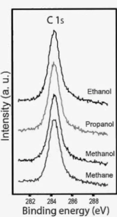
High definition C1s XPS data for the produced graphene films are presented in Figure 2.4. The data for the alcohol based graphene grown at 850
o
c
is compared to the pristine methane sourced films. Monolayer graphene displays a single peak around 284.5eV. The lack of a shoulder between 286eV to 287eV indicates that the oxygen moieties present in the precursors have no measurable effect, doping or oxidation, on the resulting graphene layer.C ls
282 284 286 288
Binding energy (eV)
Figure 2.4: C1s XPS data for alcohol and methane grown graphene. o oxyge n-doped peak was observed for pristine graphene.
SEM and optical imagery
The SEM images present homogenous and uniform films from alcohols and methane. Alcohol grown graphene was successfully transferred onto Si02/Si substrates, pro -ducing samples of size comparable to our quartz furnace tube's diameter, 3 x 3 cm 2
. Optical microscopy supports the cleanliness and continuity of the transferred graphene layers, as shown in Figure 2.6.
Raman Spectroscopy
Raman spectroscopy (Renishaw inVia) with a 514.5 nm pump laser was used to characterize the thickness and quality of the methane and alcohol grown graphene. Figure 2.7 shows the measured Raman spectra of graphene produced with methane and alcohol precursors, obtained after transfer on Si02/Si substrates. From the Raman spectra, graphene synthesized from alcohol precursors is of comparable