an author's https://oatao.univ-toulouse.fr/21808
http://doi.org/10.1109/TNS.2015.2497405
Marcelot, Olivier and Goiffon, Vincent and Raine, Mélanie and Duhamel, Olivier and Gaillardin, Marc and Molina, Romain and Magnan, Pierre Radiation Effects in CCD on CMOS Devices: First Analysis of TID and DDD Effects. (2015) IEEE Transactions on Electron Devices, 62 (6). 2965-2970. ISSN 0018-9383
Abstract—As CMOS image sensors become more and more
attractive and with high performances, it becomes possible to use CCD on CMOS devices with reasonable lengths. However, no study has been done on the radiation hardness of such CCD on CMOS devices. Therefore, we propose in this paper a first study of Charge Transfer Inefficiency (CTI) and dark current degradation under TID and DDD irradiations. To do so, test chips have been processed in conventional deep submicron CMOS imaging technologies, and characterized before and after irradiations.
Index Terms— Charge coupled devices, charge transfer,
charge, transfer inefficiency, CMOS image sensors (CIS), deep submicrometer process, trapped charge, Radiation effects
I. INTRODUCTION
harge-Coupled Devices (CCD) are widely used in space imaging applications such as CCD array or Time Delay Integration (TDI) sensors [1] - [3]. However, these devices need to be produced in specific fab, offering a CCD process. The drawbacks are a low integration, a higher cost, and the impossibility to integrate CMOS functions on-chip. Thanks to the latest advances in manufacturing process, it is now possible to achieve high performance image sensors in CMOS technology, using optimized conventional or pinned photodiodes [4] [5]. However, even with the use of CMOS image sensor (CIS) technologies, CMOS Active Pixel Sensors (APS) cannot compete with CCD in some niche applications like TDI imaging. Consequently, a very strong need for the integration of CCD devices on CMOS technology is emerging in order to combine the advantages of CMOS integration, photodiodes and pinned photodiodes, and charge transfer along long distances with high performance.
As opposed to CCD processes, CMOS imaging submicronic processes do not provide poly-silicon overlapping. The designer is supposed to follow the minimum poly-silicon gap rule which is usually larger than 200 nm. Due to the presence of this “poly-gap”, electrons located in the silicon region between two adjacent gates are controlled by a weak electric field and can be delayed or even lost during the transfer [6].
O. Marcelot, V. Goiffon, R. Molina, P. Magnan are with ISAE, Université de Toulouse, Image Sensor Research Team, 10 avenue E.Belin, F-31055, Toulouse, France.
M. Raine, O. Duhamel, M. Gaillardin are with CEA, DAM, DIF, F-91297, Arpajon, France.
Thus, the Charge Transfer Inefficiency (CTI), which measures the electrons missing after one transfer [7], is larger in CCD on CMOS devices and achieves some 10-3 [8] [9] where in pure CCD it is less than 10-5 [10] [11]. One other weakness is the lowest oxide quality compared to CCD processes, which leads to a larger number of trapped charge. An alternative is to design a buried CCD by means of a buried implantation in the CCD channel [12]. This additional implant creates a buried potential well, and electrons are thus carried away from the surface. This modification improves the transfer efficiency. Generally, imaging manufacturers do not provide this process modification, and we prefer at first not to use it in order to get results comparable with common imaging processes. Consequently, CCD on CMOS performances are, for now, lower than conventional CCD technologies. CCD on CMOS are therefore usable for a small number of poly-gates, for example in TDI.
Due to the specificity of their applications, all image sensors developed for space instruments or nuclear physics experiments [13] have to be radiation tolerant. A large amount of work has been performed on the radiation tolerance of 3T photodiodes and pinned photodiodes [13] - [18]. As a general conclusion, the Total Ionizing Dose (TID) induces traps in oxides, leading to an increased dark current, a degradation of the charge transfer efficiency, and a modification of the Full Well Capacity (FWC). As for the Displacement Damage Dose (DDD), it induces defects in silicon which degrade key photodiode parameters such as Quantum Efficiency, charge to voltage conversion gain (CVF), FWC, and increases the dark current.
Extensive studies have been performed in order to study the impact of radiations in pure CCD technology detectors [19] - [25]. As in pinned photodiodes, DDD creates bulk defects in the silicon which behave as carrier traps or emitters. Accordingly, authors concluded that DDD induces increased dark current, charge transfer inefficiency and degradation of minority carrier lifetime. TID mainly degrades oxide and especially gate oxide by creating interface states [20]. This occurrence results in an increased dark current and a change in the flatband voltage, which can seriously degrade the charge transfer efficiency in surface channel CCD [20] [22]. Despite the fact that CCD on CMOS technology is of primary interest for space remote sensing applications (based on TDI), to our knowledge, no work has been performed on the effect of radiation in CCD on CMOS devices. As CCD on CMOS
Radiation Effects in CCD on CMOS Devices:
First Analysis of TID and DDD Effects
O. Marcelot, Member, IEEE, V. Goiffon, Member, IEEE, M. Raine, O. Duhamel, M. Gaillardin, R.
Molina and P. Magnan, Member, IEEE
conventional CCD devices (silicon, silicon dioxide, poly-silicon), we expect to observe similar parameter degradations. We therefore propose in this paper to perform a first set of measurements on irradiated CCD on CMOS devices and to analyze the effect of TID and DDD on their behavior. The radiation hardness topic was not addressed in this paper, and is left for future studies.
II. EXPERIMENTAL DETAILS
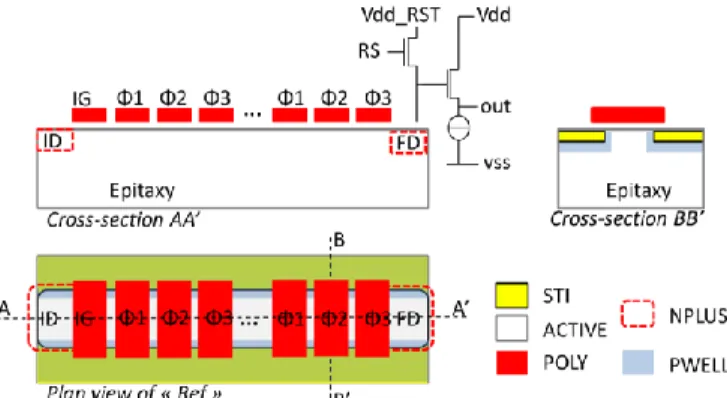
A test chip consisting of three kinds of CCD on CMOS structures is manufactured on a 180 nm imaging CMOS technology by a leading Asian company. No additional process option is used, so the CCD on CMOS is made with standard conditions and is compatible with Surface channel transport (SCCD). In the reference structure (“Ref”), in order to avoid any dark current generation due to a contact of the depleted region with the Silicon Trench Isolation (STI) edges, STI edges are enclosed within 100 nm of P-well (Fig. 1). With the aim of verifying the efficiency of this strategy, a second structure is designed (Fig. 2) with an exclusion of 100 nm of P-well from the STI (“Pwell shift”). The third structure has shorted poly-silicon gates on one side (“Poly shift”), the intent being to see if the suppression of a gate extension over the STI reduces the dark current and the interface traps impact (Fig. 2). Gates are 0.8 µm long by 1.3 µm wide, and separated by a 250 nm gap, as requested by the foundry. The CCD structures are available in 3 and 201 transfer gates. No implant is added in the CCD channel.
The CCD on CMOS device is designed to be compatible with three phases architectures. Electrons are injected by means of an injection drain and an injection gate, using the fill and spill method [26] [27]. Electrons are transferred to a floating diffusion node connected to a readout chain, similar to the ones used in CMOS imaging systems [4].
An additional test chip is designed in order to check the behavior of Buried channel CCD (BCCD) under ionizing radiation. For this specific purpose, the test chip is fabricated at a different foundry providing buried channel devices. The buried CCD test structure is designed with the same
3, with a buried implant in the CCD channel. This test chip is only employed in the TID results section.
Experimental measurements were performed at 22°C using a Cascade semi-automatic Prober and a Pulse Instrument data generator. Each analysis is executed on two dies. The main parameter characterizing the CCD device is the Charge Transfer Inefficiency (CTI), which gives the ratio of electrons missed or lost after one transfer. Indeed, due to the presence of surface states, potential barrier between gates due to the poly-gap and silicon bulk defects, electrons can be trapped and eventually re-emitted when the charge packed has moved to next gates. This causes CTI. Some of these electrons are transported in the following transfer phases, and they are called “deferred electrons”. The electrons that did not make through the transfer process at all are called “lost charge”. All CTI measurements are performed by means of two different methods. The first one is the commonly used Extended Pixel Edge Response (EPER) which consists in measuring the amount of charge emerging in the first, second, etc. transfer following the charge transfer [28] [29]. This method provides a CTI based on the number of deferred charge. EPER is applied on the 201 gates structure. The second one is based on a comparison between the number of transferred electrons after 3 gates and the number of transferred electrons after 201 gates [30]. In the following this method will be called “Compared Pixel Response (CPR)”. To do so, we assume that
Fig. 1. Cross-sectional views of the “Ref” CCD test structure and corresponding designed plan view (not to scale). ID is the injection drain, IG the injection gate, Φ1 Φ2 and Φ3 are the three CCD phases, and FD is the floating diffusion.
Fig. 2. Plan views and cross-sectional views of the “Pwell shift” (a) and “Poly shift” (b) CCD test structures (not to scale). ID is the injection drain, IG the injection gate, Φ1 Φ2 and Φ3 are the three CCD phases, and FD is the floating diffusion.
Fig. 3. Plan views and cross-sectional views of the “BCCD Ref” CCD test structures (not to scale). ID is the injection drain, IG the injection gate, Φ1 Φ2 and Φ3 are the three CCD phases, and FD is the floating diffusion.
the CTI is constant over the entire CCD device, and we measure the transferred charge at the output of the 3 gates structures and 201 gates structures:
CVF V Qtr_3G out_3G (1) CVF V Qtr_201G out_201G (2)
where ΔVout is the potential shift of the floating node and CVF is the charge to voltage conversion gain. The CTI is then calculated from the value of transferred charge of these two structures, via Equation 3:
G G
G _ out G _ out G _ out n n V V V CTI 3 201 3 201 3 1 (3)where n3G and n201G are respectively the transfer gate number in the CCD test structure containing 3 transfer gates and 201 transfer gates. The advantage of this combined method is to provide a CTI based on both deferred and lost charge.
The mean dark current measurements are also performed at 22°C, by varying the storage time on one gate from 20 µs to 180 ms.
CTI and dark current data are averaged on more than 200 measurements, with the intention of limiting errors.
In order to give an estimate of the injected electron number, the CVF of the floating node is evaluated via its dimension and the foundry capacitance model.
After a first pre-irradiation measurement sequence, some CCD on CMOS devices are irradiated at CEA, Valduc with 14.7 MeV neutrons with fluences of 3.11x10¹⁰ n/cm2 and 3.64x10¹² n/cm2, which generate a DDD of 110 TeV/g and 13120 TeV/g respectively. Other CCD on CMOS devices are irradiated at CEA, DIF with a 10 keV X-ray source in order to produce TID of 10 krad and 100 krad. All irradiations are performed unbiased, and a second measurement sequence is performed post-irradiation.
III. RESULTS
A. Before irradiation
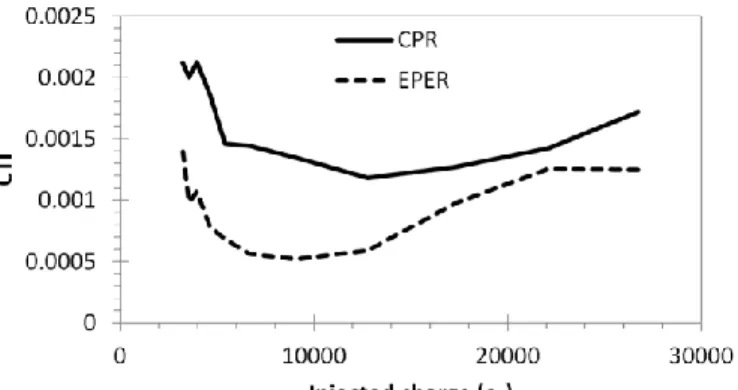
Fig. 4 shows the CTI measurements of the reference sample performed before irradiation.
From the EPER measurement (dotted line), based on deferred electrons, it can be seen that the CTI strongly decreases with the increase of charge injection until 10000 electrons. This behavior is well known in CCD and is mostly attributed to the presence of interface traps [22] [24] [31]. Indeed, the smaller the number of injected electrons, the larger the part of trapped electrons in these interface traps, and the larger the CTI. Then, the CTI increases with the increase of injected charge (from 10000 electrons), and reaches a plateau for more than 22000 electrons. It is mainly due to the large
amount of charge packets, which reduces the well potential of the channel for a high amount of electrons. CTI values measured by EPER are in the range of 5x10⁻⁴ to 1.4x10⁻³. If we look now at the CTI acquired by the method CPR proposed in this paper (straight line), the measured values are slightly larger, because this measurement takes into account the lost charge. The curve behavior is similar to the EPER one, except at very high injection where the plateau is not observed. The CTI is in the range of 1.2x10⁻³ to 2.1x10⁻³. Between 12000 and 22000 injected electrons, the difference between CTI measured by CPR and EPER is getting lower, and we can deduce that the transfer inefficiency is mainly dominated by deferred charge. For more than 22000 injected electrons, the CPR CTI is increasing again with charge injection, which suggests that more and more electrons are lost.
Fig. 5presents a comparison of CTI measured via the CPR and the EPER methods for the three different CCD on CMOS designs.
In spite of shorted poly gates used to reduce the interface traps, no reduction of CTI is visible on the sample “Poly shift”. Two assumptions can explain this observation. First, the P-well enclosure of STI may be efficient enough to avoid charge trapping. Second, the CTI may be dominated by the gate oxide trapping and the only alternative would be to use a buried channel transport. The curves of the sample “Pwell
Fig. 4. CTI vs. charge injection in the “Ref” structure. The CTI is evaluated using the CPR method and using the EPER method
Fig. 5. Comparison of CTI against charge injection between the three designed structures. The CTI is evaluated using the CPR and the EPER method.
CTI. At low injection, the CTI of “Pwell shift” measured via the two methods is strongly increased, which shows that the number of deferred charge increases a lot when STI edges are not passivated. However, at high injection the CTI of this design is still higher, mainly due to the increase of lost charge as the EPER CTI is kept low. One assumption could be that when the charge packet is increasing, so is its volume, and it interacts with more STI traps located on vertical STI edges (approximately 300 nm deep).
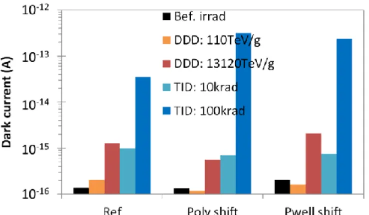
The dark current measurements are shown in Fig. 6. Before irradiation, the dark current measured on the samples “Ref” and “Poly shift” are around 140 aA. Again, there is no strong difference between the two designs despite what could be expected. The dark current of the sample “Pwell shift” is larger, as expected, around 210 aA.
The well capacity of the gates could not be measured, because of the saturation of the readout chain. Indeed, the amount of injected electrons is increased as much as possible and a saturation of the output signal is observed at 35000 e-/µm². This saturation corresponds to the readout chain saturation and it is therefore possible to state that the well capacity is higher than 35000 e-/µm².
B. TID effects
To observe Total Ionizing Dose effect on CCD on CMOS devices, the structures are irradiated with 10 keV X-ray at 10 krad (SiO2) and at 100 krad (SiO2).
CTI are measured after irradiation and some of the results are presented in Fig. 7. The CTI of the “Ref” sample increases a lot with TID. As for pure surface channel CCD [20], TID impacts strongly the transfer efficiency because of an increase of surface states and a flatband voltage change. At 100 krad we did not succeed in measuring the CTI of 201 gates structures for less than 12000 electrons. Therefore, CTI measurements with EPER method at 100 krad are also conducted on the 3 gates structure.
Dark current measurements are shown in Fig. 6. As expected, these measurements show a strong increase of dark current with TID. At 100 krad the dark current achieves high values, depending on the design. In particular, the “poly shift”
explain for now.
Considering these TID results, the use of CCD on CMOS devices will be problematic in space applications. One possibility would be to use buried channel CCD in order to avoid the gate oxide trapping.
With the intention to check it, we designed a different test chip fabricated in another CMOS process allowing buried channel devices. This test chip has CCD structures with a design similar to the “Ref” CCD test structure (Fig. 3), except a Buried CCD layer implanted in the CCD channel. The BCCD structure has 3 and 201 transfer gates, and the same methodology was applied for measurements. After a first measurement sequence, the BCCD structures are irradiated with 10 keV X-ray at 10 krad (SiO2) and at 100 krad (SiO2) in order to create TID. The Fig. 8 is showing the transfer inefficiency measurements.
Before irradiation, CTI measured in BCCD is comparable to CTI measured in SCCD (Fig 4 and Fig. 8). In contrary to what we could expect, the performances in BCCD are not better, probably because we used a different foundry compared to SCCD, and because the buried channel process is not enough optimized for this purpose. After irradiation of the BCCD, the CCD structure is still operational and it is still possible to
Fig. 6. Comparison of mean dark current for the three designs before and after irradiation.
Fig. 7. Comparison of CTI against charge injection before and after TID irradiation for the “Ref” structure. The CTI is evaluated using the CPR and EPER method.
Fig. 8. Comparison of CTI against charge injection before and after TID irradiation for the BCCD “Ref” structure, processed in a different foundry. The CTI is evaluated using the CPR and EPER method.
measure the charge transfer even on the 201 gates structures and at 100 krad. From this first observation, one can conclude that the BCCD structure is more radiation tolerant than the SCCD one. At 10 krad, we can see a small increase of CTI. At 100 krad, the CTI increases by a factor of 2, however at high injection it remains lower than in SCCD. Al low injection, the EPER CTI stays relatively flat, in contrary to the CPR CTI. This suggests that at 100 krad the ratio of lost charge becomes higher with this design and technology. The buried channel structure is not radiation tolerant as it could be expected. This is probably because the STI edges are in contact with the BCCD implant. This should be taken into account for a future and improved design.
Dark current measurements on BCCD structures are also performed and are presented in Fig. 9. Before irradiation the BCCD dark current is higher than the SCCD one because the process is different. However if we look at the dark current behavior after irradiation, we can see that the buried channel is much more radiation tolerant: the dark current is increased by x6 in BCCD instead of x250 in SCCD. Indeed, as electrons are carried in a buried channel away from the degraded surface oxide the dark current increase is relatively contained. This performance should be improved by moving STI edges away from the BCCD implant.
To conclude, ionizing radiation strongly degrades the performance of CCD on CMOS devices. Although CTI degradation in buried channel devices is much lower than that of surface channel devices, the operation of CCD on CMOS devices in general will be compromised in harsh ionizing radiation environment.
C. DDD effects
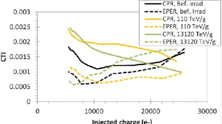
The three different surface channel CCD designs are also irradiated with neutrons in order to create displacement damage in silicon. The CTI measurements performed on the sample “Poly shift” are shown in Fig. 10.
Small differences between non-irradiated and irradiated curves are visible and are attributed to measurement artifacts. As opposed to TID effects, DDD does not lead to an obvious transfer performance degradation, and the CCD on CMOS
device is still functional after 13120 TeV/g. Results obtained are quite similar for all three designs, and no clear CTI degradation is visible after irradiation.
This performance could be expected, as surface channel CCD on CMOS structures are limited by oxide trapping, and much less by volume defects. Indeed, in this configuration, the potential monotony decreases from the surface to the bulk, and carrier charge packets are confined to the vicinity of the surface. As neutrons create bulk defects, the surface channel transport should not degrade until a given DDD. Besides, in pure CCD technology, transfer inefficiency increases are generally observed in buried channel CCD devices [19] [21] [22].
Dark current measurements are also performed and are shown in Fig. 6. The 110 TeV/g DDD induces a dark current increase for the reference design and a smaller dark current decrease for the other two designs. This unexpected result is attributed to measurement artifacts. The highest DDD induces a clear dark current increase by a factor of 10, because of the creation of bulk defects, with small differences depending on the design. The design with a recessed P-well (“Pwell shift”) has the largest dark current, while the design with poly shift seems to be more tolerant. In parallel, the mean dark current increase has also been estimated using the Srour formalism [32]. The depleted volume is taken as the gate active area times 2 µm of depleted depth. At 110 TeV/g the mean dark current increase is estimated at 7 aA, and at 13120 TeV/g it is estimated at 850 aA. These estimations are in a good agreement with the measured dark current increase.
IV. CONCLUSION
In this paper we study three different designs of CCD structures manufactured on a CMOS technology before and after TID and DDD irradiations. Results obtained before irradiation show that the STI edges in the CCD channel must be covered by P-well in order to limit dark current generation and CTI degradation. Shorting the gate on one side does not help because the P-well enclosure of STI may be efficient enough to avoid charge trapping or because the CTI is probably limited by the gate oxide trapping. Measured CTI are
Fig. 9. Comparison of mean dark current for SCCD and BCCD before and after irradiation.
Fig. 10. Comparison of CTI against charge injection before and after DDD irradiation for the “Poly shift” structure. The CTI is evaluated using the CPR and the EPER method.
strongly impacts the transfer efficiency. At 100 krad the CCD on CMOS device is still functional, however the CTI is multiplied by 5 – 10, and the dark current is increased by a factor of about 103. A buried channel CCD structure is also investigated under TID and is showing a better radiation tolerance. However, CTI obtained at 100 krad in buried channel mod are still too high. Therefore the CCD on CMOS usage seems to be compromised in radiation application where TID is dominating. The surface channel CCD is more tolerant to Displacement Damage Dose, as the CTI is not affected until 13120 TeV/g for all three structures and the dark current is only increased by a factor of 10. As a conclusion, CCD on CMOS devices as they were designed for this paper cannot be used in space radiation environment, because maximum TID specifications are usually inferior to 100 krad. However, the surface channel CCD on CMOS devices could be used in radiation environment where DDD is dominating.
REFERENCES
[1] S.E. Holland, D.E. Groom, N.P. Palaio, R.J. Stover, M. Wei, “Fully-Depleted, Back-Illuminated Charge-Coupled Devices Fabricated on High-Resistivity Silicon,” IEEE Trans. Electron Devices, vol. 50, no. 1, pp. 101-114, Jan. 2003.
[2] K. Fife, A.E Gamal, H.S.P Wong, “A Multi-Aperture Image Sensor With 0.7 µm Pixels in 0.11 µm CMOS Technology,” IEEE J. Solid-State Circuits, vol. 43, no. 12, pp. 2990-3005, Dec. 2008.
[3] G. Lepage, J. Bogaerts, G. Meynants, “Time Delay Integration in CMOS image sensors,” IEEE Trans. Electron Devices, vol. 56, no. 11, pp. 2524-2533, Nov. 2009.
[4] A.J.P. Theuwissen, “CMOS image sensors: State-of-the-art,” Solid St. Electron., vol. 52, pp. 1401-1406, May 2008.
[5] P. Lee, R. Gee, M. Guidash, T. Lee, and E. R. Fossum, “An active pixel sensor fabricated using CMOS/CCD process technology,” in Proc. IEEE Workshop on CCDs and Advanced Image Sensors, Apr. 1995, pp. 115– 119
[6] N. Mutoh, S. Kawai, T. Yamada, Y. Kawakami, T. Nakano, K. Orihara, and N. Teranishi, “Driving Voltage Reduction of Shift Registers in IT-CCD Image Sensors,” in Proc. IEEE, Jun. 1997.
[7] M.F. Tompsett, “The Quantitative Effects of Interface States on the Performance of Charge-Coupled Devices,” IEEE Trans. Electron Devices, vol. ED-20, no. 1, pp. 45-55, Jan. 1973.
[8] J. borg and J. Johansson, “Evaluation of a Surface-Channel CCD Manufactured in a Pinned Active-Pixel-Sensor CMOS Process,” IEEE Trans. Electron Devices, vol. 58, no. 8, pp. 2660-2664, Aug. 2011. [9] K. Fife, Abbas El Gamal and H.-S. Philip Wong, “A 0.5p,m Pixel
Frame-Transfer CCD Image Sensor in 110nm CMOS,” in Proc. IEEE, Feb. 2007, pp. 1003-1006.
[10] R. Hoople, “Characteristics of Submicrometer Gaps in Buried-Channel CCD Structures,” IEEE Trans. Electron Devices, vol. 38, no. 5, pp. 1175-1181, May 1991.
[11] T. Lee, T. J. Tredwell, B. C. Burkey, T. M. Kelly, R. P. Khosla, D. L. Losee, R. L. Nielsen, and W. C. McColgin, “A 360000 Pixel Charge-Coupled Color-Image Sensor for Imaging Photographic Negative,” IEEE Trans. Electron Devices, vol. ED-32, no. 8, pp. 1439-1445, Aug. 1985.
[12] M. J. Howes, D. V. Morgan, Wiley. (1979). Charge-coupled Devices and System.
[13] M. Deveaux, G. Claus, G. Deptuch, W. Dulinski, Y. Gornushkin, and M.Winter, “Neutron radiation hardness of monolithic active pixel sensors for charged particle tracking,” Nucl. Instr. Meth. A, vol. 512, pp. 71–76, Oct. 2003.
[14] G. R. Hopkinson, “Radiation effects in a CMOS active pixel sensor,”IEEE Trans. Nucl. Sci., vol. 47, no. 6, pp. 2480–2484, Dec. 2000 [15] M. Cohen and J.-P. David, “Radiation-induced dark current in CMOS active pixel sensors,” IEEE Trans. Nucl. Sci., vol. 47, no. 6, pp. 2485– 2491, Dec. 2000.
generation in proton-irradiated CMOS active pixel sensors,” IEEE Trans. Nucl. Sci., vol. 49, no. 3, pp. 1513–1521, Jun. 2002
[17] C. Virmontois, V. Goiffon, P. Magnan, S. Girard, C. Inguimbert, S. Petit, G. Rolland, and O. Saint-Pe, “Displacement damage effects due to neutron and proton irradiations on CMOS image sensors manufactured in deep sub-micron technology,” IEEE Trans. Nucl. Sci., vol. 57, no. 6, pp. 3101–3108, Dec. 2010.
[18] V. Goiffon, C. Virmontois, P. Magnan, S. Girard, and P. Paillet, “Analysis of Total Dose-Induced Dark Current in CMOS Image Sensors From Interface State and Trapped Charge Density Measurements”, Nucl. Sci., vol. 57, no. 6, pp. 3087–3094, Dec. 2010
[19] N. S. Saks, “Investigation of bulk electron traps created by fast neutron irradiation in a buried n-channel CCD,” IEEE Trans. Nucl. Sci., vol. NS-24, pp. 2153–2157, Dec. 1977
[20] T. Roy, S.J. Watts and D. Wright, “Radiation Damage Effects on Imaging Charge Coupled Devices”, Nucl. Inst. Meth., A275, pp. 545-557, Mar. 1989
[21] A. Holland, A. Holmes-Siedle, B. Johlander, and L. Adams, “Techniques For Minimizing Space Proton Damage In Scientific Charge Coupled Devices”, IEEE Trans. Nucl. Sci., vol. 38, pp. 1663–1670, Dec 1991
[22] J. R. Janesick ; G. B. Soli ; T. S. Elliott and S. A. Collins, "Effects of proton damage on charge-coupled devices", Proc. SPIE 1447, Charge-Coupled Devices and Solid State Optical Sensors II, 87, Jul. 1991 [23] G. R. Hopkinson, C. J. Dale, and P. W. Marshall, “Proton Effects in
Charge-Coupled Devices”, IEEE Trans. Nucl. Sci., vol. 43, pp. 614–627, Apr 1996
[24] T. Hardy, R. Murowinski, and M. J. Deen, “Charge Transfer Efficiency in Proton Damaged CCD’s”, IEEE Trans. Nucl. Sci., vol. 45, pp. 154– 163, Apr 1998
[25] G. R. Hopkinson, “Proton Damage Effects on P-Channel CCDs”, IEEE Trans. Nucl. Sci., vol. 46, pp. 1790–1796, Dec 1999
[26] G. Prigozhin, and B. Burke, “CCD Charge Injection Structure at Very Small Signal Levels,” IEEE Trans. Electron Devices, vol. 55, no. 8, pp. 2111-2120, Aug. 2008.
[27] M.F. Tompsett, “Surface Potential Equilibration Method of Setting Charge in Charge-Coupled Devices,” IEEE Trans. Electron Devices, vol. ED-22, no. 6, pp. 305-309, Jun. 1975.
[28] R.W. Brodersen, D.D. Buss, and Al.F. Tasch; “Experimental Characterization of Transfer Efficiency in Charge-Coupled Devices,” IEEE Trans. Electron Devices, vol. ED-22, no. 2, pp. 40-46, Feb. 1975. [29] A. Waczynski, E. J. Polidan, P. W. Marshall, R. A. Reed, S. D. Johnson,
R. J. Hill, G. S. Delo, E. J. Wassell, and E. S. Cheng, “A Comparison of Charge Transfer Efficiency Measurement Techniques on Proton Damaged n-Channel CCDs for the Hubble Space Telescope Wide-Field Camera 3,” IEEE Trans. Nuc. Sci., vol. 48, no. 6, pp. 1807-1814, Dec. 2001.
[30] O. Marcelot, M. Estribeau, V. Goiffon, P. Martin-gonthier, F. Corbière, R. Molina, S. Rolando, and P. Magnan, “Study of CCD Transport on CMOS Imaging Technology: Comparison Between SCCD and BCCD, and Ramp Effect on the CTI”, IEEE Trans. Electron Devices, vol. 61, no. 6, pp. 844-849, Mar 2014
[31] R.W. Brodersen, D.D. Buss, and Al.F. Tasch; “Experimental Characterization of Transfer Efficiency in Charge-Coupled Devices,” IEEE Trans. Electron Devices, vol. ED-22, no. 2, pp. 40-46, Feb. 1975 [32] J. R. Srour, and D. H. Lo, “Universal Damage Factor for
Radiation-Induced Dark Current in Silicon Devices”, IEEE Trans. Nucl. Sci., vol. 47, pp. 2451–2459, Dec 2000