HAL Id: pastel-00749642
https://pastel.archives-ouvertes.fr/pastel-00749642
Submitted on 8 Nov 2012
HAL is a multi-disciplinary open access archive for the deposit and dissemination of sci-entific research documents, whether they are pub-lished or not. The documents may come from teaching and research institutions in France or abroad, or from public or private research centers.
L’archive ouverte pluridisciplinaire HAL, est destinée au dépôt et à la diffusion de documents scientifiques de niveau recherche, publiés ou non, émanant des établissements d’enseignement et de recherche français ou étrangers, des laboratoires publics ou privés.
Metamaterial inspired improved antennas and circuits
Davi Bibiano Brito
To cite this version:
Davi Bibiano Brito. Metamaterial inspired improved antennas and circuits. Electromagnetism. Télé-com ParisTech, 2010. English. �pastel-00749642�
UNIVERSIDADE FEDERAL DO RIO GRANDE DO NORTE
TELECOM PARISTECH
METAMATERIAL INSPIRED IMPROVED
ANTENNAS AND CIRCUITS
DAVI BIBIANO BRITO
NATAL, RN - BRAZIL
DECEMBER 2010
UNIVERSIDADE FEDERAL DO RIO GRANDE DO NORTE
TELECOM PARISTECH
Metamaterial Inspired Improved Antennas and
Circuits
Davi Bibiano Brito
Natal, RN - Brazil
December 2010
D.Sc. Dissertation presented to the
UFRN Graduate Program in Electrical and Computer Engineering (Area: Telecommunications) and Telecom ParisTech Graduate Program in Electronics and Telecommunications as part of the requirements to obtain the title of Doctor of Science.
Metamaterial Inspired Improved Antennas and Circuits
A Thesis Presented to The Academic Faculty
by
Davi Bibiano Brito
In Partial Fulfillment Of the Requirements for the Degree Doctor of
Science in Electrical Engineering
Advisor:
Prof. Dr. Adaildo Gomes d’Assunção (UFRN)
Advisor:
Prof. Dr. Xavier Begaud (Telecom ParisTech)
Co-Advisor: Prof. Dr. Humberto César Chaves Fernandes (UFRN)
Examiner: Prof. Dr. José Ricardo Bergmann, (PUC-Rio)
Examiner: Prof. Dr. Tan-Phu Vuong (INPG-Grenoble)
Examiner: Prof. Dr. Gervásio Protásio dos Santos Cavalcante (UFPA)
Examiner: Prof. Dr. Bernard Huyart (Telecom ParisTech)
Acknowledgements
Foremost, I would like to express my sincere gratitude to my advisors Prof. Adaildo Gomes D’Assunção, Prof. Xavier Begaud and Prof. Humberto César Chaves Fernandes for the continuous support of my Ph.D study and research, for their patience, motivation, and immense knowledge. Their guidance helped me in all the time of research and writing of this thesis. Besides my advisors, I would like to thank my fellow labmates at UFRN and Telecom ParisTech for the stimulating discussions and for all the fun we have had in the last four years.
Last but not the least, I would like to thank my family for all their love and encouragement. My Grandparents Rafael, Dione and Maria for their love and support. My Uncle José for his help. For my parents Dacio e Roberta (for giving birth to me at the first place) who raised me with a love of science and supported me in all my pursuits. And most of all for my loving, supportive, encouraging, and patient Pollyana whose faithful support during the final stages of this Ph.D. is so appreciated. Thank you all.
List of Publications
D. B Brito, A. G. D'Assuncao, H. C. C. Fernandes and X. Begaud “Complementary Split Ring Resonator Stop-Band Filter” SBMO/IEEE MTT-S International Microwave and Optoelectronics Conference, 2011, Natal. Technical Program, 2011.
D. B. Brito, X. Begaud, A. G. D'Assuncao, and H. C. C. Fernandes, “Ultra wideband monopole antenna with Split Ring Resonator for notching frequencies”, EuCAP 2010. 4th European Conference on Antennas and Propagation, pp. 1 - 5, Barcelona, Espanha, Abril 2010.
D. B. Brito, X. Begaud, A. G. D'Assuncao, and H. C. C. Fernandes, “Ultra Wideband Monopole Antenna using Split Ring Resonator”, COSTic0803 3rd Management Committee/Working Group, Meeting and Workshop, Atenas, Grécia, Outubro 2009.
D. B. Brito, H. C. C. Fernandes, “Unilateral Fin Line Directional Coupler”. International Journal of Infrared and Millimeter Waves, v. 28, p. 651-661, Setembro 2007.
Table of Contents
Chapter 1 Introduction ... 15
Chapter 2 Metamaterials ... 16
2.1 Metamaterials Overview... 16
2.2 Electromagnetic Wave Propagation in a Metamaterial Media ... 21
2.3 Artificial Materials ... 24
2.4 Bianisotropic Media ... 29
2.4.1 Double-Negative and Indefinite Media ... 31
2.4.2 Photonic and Electromagnetic Crystal ... 32
2.5 Summary... 33
Chapter 3 Frequency Selective Surfaces ... 34
3.1 FSS Element Types ... 36
3.2 Electromagnetic Wave Propagation in a Metamaterial Media ... 37
3.2.1 Infinite FSS Arrays ... 38
3.2.2 Finite FSS Arrays ... 38
3.3 Metamaterial FSSs ... 39
3.4 Antenna Bandwidth augmentation ... 41
3.5 Summary... 42
Chapter 4 Planar Antennas and Microtstrip Filters with CSRR Parasitic Structures ... 43
4.1 Ultra Wideband Monopole Antenna with Split Ring Resonator as Filter ... 42
4.1.1 Complementary Split Ring Resonator ... 49
4.1.2 Simulation and Experimental Results ... 50
4.2 CSRR Stop Band Filter ... 61
4.3 Summary... 64
Chapter 5 Microstrip Antennas with HIS Ground Plane ... 66
5.1 High Impedance Surfaces ... 67
5.2 Microstrip Patch Antenna with HIS Ground Plane ... 69
5.3 Suspended U-Slot antenna on HIS Substrate ... 77
5.4 Summary... 80
Chapter 6 Fabry-Pérot Antennas ... 82
6.1 Fabry-Pérot Interferometer ... 82
6.2 The Fabry-Pérot Antenna ... 84
6.2.1 Fabry-Pérot Patch Antenna ... 85
6.2.2 Fabry-Pérot Suspended U-Slot Antenna ... 89
6.3 Summary... 92
Chapter 7 Conclusions ... 93
References ... 95
List
c CSRR DNG DPS EBG ENG ε0 εeff εr FSS FP HIS LHM λ λ0 λg MNG µ0 µeff µr PCB PEC RF SNG SRR σ TW ωt of A
Nab Mag Velo Com Elec Dou Dou Elec Elec Epsi Free Effe Rela Freq Fabr Mag High Wav Left Wav Free Guid Mu-Free Effe Rela Inde Prin Perf Rad Poyn Sing Split Con Thin AngAcrony
bla operator gnetic field ocity of ligh mplementary ctric displac uble-Negativ uble-Positive ctric field ctromagneti ilon-negativ e space perm ective permi ative permit quency Sele ry-Pérot gnetizing fie h Impedanc ve vector t Handed M velength e space wav ded wavelen -Negative e space perm ective perme ative perme ex of refract nted Circuit fectly Electr io Frequenc nting vector gle-Negative t Ring Reso nductivity of n-Wire gular frequenyms a
ht y Split Ring cement field ve e c Band-Gap ve mittivity ittivity ttivity ective Surfac eld ce Surface Metamaterial velength ngth meability eability ability tion Board rically Cond cy r e onator f the metal ncyand Sy
g Resonator d p ces ductingymbo
rols
List of Figures
Figure. 2.1 Diagram showing the Poynting vector of an electromagnetic wave. On left
normal materials, and on the right metamaterials ... 17
Figure. 2.2 Ray diagram of interface between n>0 and n<0 media ... 18
Figure. 2.3 A diagram showing the possible domains of electromagnetic materials and wave refraction having the same sign. Waves are refracted positively in conventional materials and negatively in LHM... 19
Figure. 2.4 Ray diagram showing the direction of wave propagation ... 20
Figure. 2.5 The geometry of a generic artificial dielectric ... 20
Figure. 2.6 The geometry of wire medium: a lattice of parallel conducting thin wires ... 25
Figure. 2.7 Metamaterials constructed with common dielectrics and metals: (a) negative permittivity and positive permeability, (b) negative permeability and positive permittivity, and (c) double negative media DNG [15] ... 25
Figure. 2.8 Equivalent circuit model for the Split Ring Resonator, double and simple rig configurations ... 27
Figure. 2.9 Theoretical results for: (a) permittivity using a SRR and (b) permeability using a thin wire ... 28
Figure. 2.10 Bianisotropic particles: (a) chiral, (b) omega, and (c) double chiral ... 29
Figure. 2.11 Realization of DNG material at microwave frequencies ... 30
Figure. 2.12 The blue-green color on several species of butterflies is caused by the nanoscale structure of the insects’ wings ... 31
Figure. 2.13 The first photonic crystal with a complete band gap [19] ... 32
Figure. 2.14 Ultra wideband Bowtie antenna with HIS substrate ... 32
Figure 3.1 Electron in the plane oscillates due to the force exerted by incident wave resulting in low transmittance ... 35
Figure 3.2 Electron is constrained to move and hence unable to absorb energy resulting in high transmittance ... 35
Figure 3.3 Metal screen irradiated by a normally incident plane wave [1]... 36
Figure 3.4 Basic FSS geometries: The patch-array produces a capacitive response, whereas the array of slots is inductive. ... 37
Figure 3.5 The four major groups of FSS elements. These elements may be used to construct band stop filter type FSS arrays. Elements are ordered from most narrow banded on the left to most wide-banded on the right [24] ... 38
Figure 3.7 Superior view of a high impedance surface, with patches connected to the
ground plane with metal cylinders [32] ... 40
Figure 3.6 A corrugated reactive surface acting as an AMC ... 40
Figure 3.8 Origin of the equivalent circuit elements left and equivalent circuit model for the high-impedance surface right ... 41
Figure 4.1 Ultra wideband and UN-II spectrum ... 43
Figure 4.2 Circular microstrip monopole antenna, the gray region denotes a conductor material ... 46
Figure. 4.3 (a) Return loss and (b) Smith Chart results for the microstrip circular monopole antenna ... 47
Figure 4.4 Circular microstrip monopole antenna with improved ground plane, where the gray region denotes a conductor material ... 48
Figure 4.5 Return loss for the improved microstrip circular monopole antenna ... 48
Figure 4.6 Geometries and equivalent circuit of a SRR and a CSRR, where the gray region denotes a conductor material ... 50
Figure 4.7 UWB antenna with CSRR top view and the CRSS structure bottom view: the gray region denotes a conductor material ... 51
Figure 4.8 Monopole antenna with different CSRR configurations ... 51
Figure 4.9 Return loss for different CSRR configurations, red microstrip line top center, green patch’s center and blue patch’s right center... 52
Figure 4.10 Constructed antenna ... 53
Figure 4.11 LPKF ProtoMat® printed circuit board prototyping machine ... 54
Figure 4.12 Return loss for the microstrip circular monopole antenna, in red color measured and in blue simulated results ... 55
Figure 4.13 Realized gain 3D pattern at: (a) 4GHz, (b) 5.9GHZ and 6.5 GHz ... 55
Figure 4.14 Anechoic chamber utilized in the measurements ... 56
Figure 4.15 Measurement schema used to determine the radiation pattern ... 57
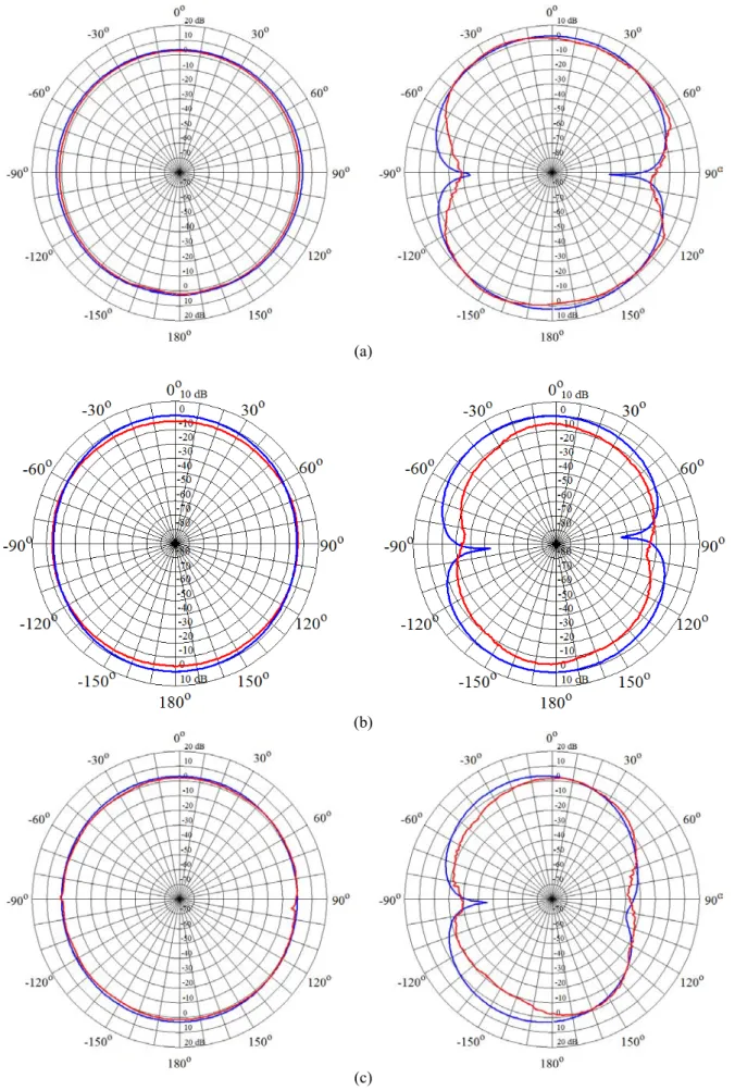
Figure 4.16 Farfield radiation patterns, E-plane, on left, results and H-plane, on right, results: (a) 4GHz, (b) 5.9 GHZ and 6.5GHz, blue simulated and red measured ... 58
Figure 4.17 FCC mask ... 59
Figure 4.18 FCC pulse ... 59
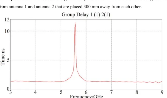
Figure 4.19 Return loss for the monopole antenna with CSRR filter inserted in the conductor patch, green curve antenna exited with UWB pulse and red curve Gaussian pulse ... 60
Figure 4.20 Group delay from two microstrip monopole antenna with CSRR filter inserted
in the conductor patch ... 60
Figure 4.21 CSRR stop band filter top. The gray region denotes a conductor material ... 62
Figure 4.22 CSRR geometries. The gray region denotes a conductor material ... 62
Figure 4.23 Simulated S11 and S21 parameters for the metamaterial based stop band with single CSRR ... 63
Figure 4.24 Three-period CSRR stop band filter, the gray region denotes a conductor material ... 64
Figure 4.25 CSRR based filter prototype ... 64
Figure 4.26 S11 (a) and S21 (b) parameters for the metamaterial-based stop band filter with three CSRRs etched do the ground plane: blue simulated and red measured .. 65
Figure 5.1 Cross-section of a high-impedance surface ... 67
Figure 5.2 A patch antenna on a metal ground plane ... 68
Figure 5.3 A patch antenna embedded in a high-impedance ground plane ... 69
Figure 5.4 HIS superior view on the left and transversal cut on the right ... 69
Figure 5.5 Reflection coefficient for the mushroom type HIS ... 71
Figure 5.6 Patch antenna inserted in the HIS medium ... 72
Figure 5.7 Surface current at 13.23 GHz in the bandgap frequency center ... 72
Figure 5.8 S11 simulation for patch antennas on two different ground planes ... 73
Figure 5.9 Constructed structure right superior front view and left superior back view ... 74
Figure 5.10 LPKF MiniContac RS ... 74
Figure 5.11 Return loss simulated and measured for the patch antenna on a high-impedance ground plane ... 75
Figure 5.12 Farfield realized gain radiation patterns for the, E-plane on the left and H-plane on the left, blue simulated and red measured results: (a) 12.75 GHz, (b) 12.95 GHz and (c) 13.15 GHz ... 76
Figure 5.13 Reflection coefficient for the mushroom type HIS ... 77
Figure 5.14 U-slot antenna and its dimensions ... 78
Figure 5.15 Suspended U-Slot antenna backed by a HIS medium ... 78
Figure 5.16 Constructed prototype right superior front view and left superior back view .. 79
Figure 5.17 Simulated and measured return loss for the suspended U-slot antenna on a HIS ground plane ... 79
Figure 5.19 Farfield realized gain radiation patterns for the, E-plane on the left and H-plane on the left, blue simulated and red measured results: (a) 3.75 GHz, (b) 4.66
GHz and (c) 5.1 GHz ... 81
Figure 6.1 Illustration of the phenomenon due to the multiple reflections and leaky waves ... 82
Figure 6.2 Graphical representation of a plane light wave with amplitude A(i) focusing on a plate with flat and parallel surfaces. The nth reflected beam is represented by ap(r) while the nth transmitted beam is represented by ap(t) ... 83
Figure 6.3 Positioning of the Fabry-Pérot when allocated in a collimated space ... 84
Figure 6.4 Square FSS used as the antenna superstrate ... 85
Figure 6.5 Fabry-Pérot patch antenna prototype ... 86
Figure 6.6 Return loss for the Fabry-Pérot patch antenna ... 86
Figure 6.7 Fabry-Pérot patch antenna mounted in the anechoic chamber ... 87
Figure 6.8 Realized gain for the Fabry-Pérot patch antenna E-plane on the left and H-plane on the left: (a) 12.7 GHz, (b) 12.9 GHz and (c) 13.1. Blue simulated and red measured resuts ... 88
Figure 6.9 Constructed Fabry-Pérot suspended U-slot antenna ... 89
Figure 6.10 Fabry-Pérot suspended U-slot antenna mounted in the anechoic chamber ... 90
Figure 6.11 Return loss for Fabry-Pérot the suspended U-slot antenna ... 90
Figure 6.12 Realize gain radiation pattern: (a) 3.6 GHz, (b) 4.4 GHz and (c) 5.5 GHz. The E-plane is on the left and H-plane is on the left. Blue simulated and red measured results ... 91
List of Tables
Abstract
Metamaterials have attracted a great amount of attention in recent years mostly due to their exquisite electromagnetic properties. These materials are artificial structures that exhibit characteristics not found in nature. It is possible to obtain a metamaterial by combining artificial structures periodically. We investigated the unique properties of Split Ring Resonators, High impedance Surfaces and Frequency Selective Surfaces and composite metamaterials. We have successfully demonstrated the practical use of these structures in antennas and circuits. We experimentally confirmed that composite metamaterials can improve the performance of the structures considered in this thesis, at the frequencies where electromagnetic band gap transmission takes place.
Keywords: Left-Handed Material, Metamaterial, Split Ring Resonator, Negative Permittivity,
Negative Permeability, High Impedance Surface, Frequency Selective Surface, Electromagnetic Band Gap, Negative Refraction, Fabry-Pérot.
Chapter 1
Introduction
Recently developments in electromagnetics in the radio frequency to optical spectral ranges and novel fabrication techniques offer a great number of exciting new applications. These structures are called metamaterials and they have electromagnetic characteristics that do not occur or are not readily available in natural materials.
The purpose of this thesis is to develop new structures, for communication systems that can provide improved functionality and performance. The great potential of metamaterials to develop such novel structures offers an alternative with potential to overcome limitations of current solutions. In this context metamaterials is a breakthrough, mainly to their exquisite material properties and ability to guide and control electromagnetic waves in a way that natural occurring materials cannot.
The thesis is organized into seven chapters. Chapter 2 presents the general theory of metamaterials that enables its characterization, including the behavior of electromagnetic waves explained through the Maxwell`s equations. Metamaterials, which have special optical properties such as a negative refractive index, are described. Metamaterials examples like the Split Ring Resonator (SRR) and the High Impedance Surface (HIS) that will be used in this thesis are presented.
In Chapter 3 the Frequency Selective Surfaces (FSS) are studied with a brief stated of art, types and forms of the most used structures and some applications are presented. The typical behavior of the most common element types available is discussed. The Frequency Selective Surface theory is considered starting with a comparison of available elements to the metamaterial FSS variants. Finally this section ends with a discussion of wideband radiating arrays.
Chapter 4 describes the use of a Complementary Split Ring Resonator (CSRR) in two metamaterials applications; in the first the CSRR is placed as a parasite element in the conductor patch of a circular planar monopole. This metamaterial structure is used as a stop
band filter for blocking the Unlicensed National Information Infrastructure (UN-II) band between 5 GHz to 6 GHz. The second application is a microstrip filter that is used as an alternative for blocking the UN-II band. The band-notched characteristic is achieved by etching a CSRR structure in the ground plane of a microstrip transmission line. It has been demonstrated that CSRR etched in the ground plane of a planar transmission media (microstrip) provides a negative effective permittivity to the structure.
In Chapter 5 a HIS metallic electromagnetic structure is used as ground plane in two directive antennas, a patch antenna and a suspended U-Shaped antenna. This structure is characterized by having high surface impedance. The HIS does not support propagating surface waves, and it reflects electromagnetic waves with no phase reversal, which can be used to improve the antennas performance.
Chapter 6 describes the use of the Fabry-Pérot (FP) optical concept as an alternative to produce highly directive antennas. This FP medium is formed employing a HIS as a metamaterial substrate and a FSS as a partially reflecting surface (PRS) superstrate. The used antennas are those described in Chapter 5. This configuration leads to single feed and low profile highly directive antennas. In addition some optical concepts are presented for a better understanding. Chapter 7 presents the conclusions and perspectives for future works.
Chapter 2
Metamaterials
There have been a large number of definitions for metamaterials [1-8], they can be generally defined as a class of ‘‘artificial’’ media, exhibiting extraordinary electromagnetic properties that cannot be found in natural ones [1]. The name given to this structurally altered material is based on the Greek µετά (meta) that means “beyond”. The subject of metamaterials has seen many exciting applications and has drawn considerable attention from many communities worldwide. The interest can be explained by the fact that the physicists normally studies the way nature works while engineers try to apply the knowledge and metamaterials can be place in between science and engineering.
From the point of view of fundamental science nothing is new in metamaterials theory. Throughout this chapter, it will be shown that metamaterials can be understood by using well-known theoretical tools from the classical electromagnetic theory, however, almost all new applications arising from metamaterial concepts can be understood by using more traditional approaches, without the need to invoke these new metamaterial concepts.
2.1 Metamaterials Overview
During the research process to write this document the first attempt to explore the concept of “artificial” materials appears back to 1898 when J. C. Bose [9] conducted the first microwave experiment on twisted structures, geometries that were essentially artificial chiral1 elements by today’s terminology. In 1905, Lamb [10] theorized the existence of backward waves that are associated with reflection directions based on the signs of permittivity and permeability. Since these researches, artificially arranged complex materials have been the subject of research worldwide.
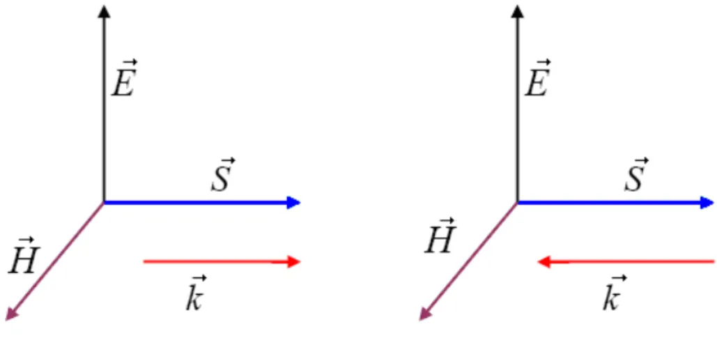
A key feature of these artificial materials is the negative refraction, that some titles leads to the given name "left handed materials" (LHM), materials that refract electromagnetic waves in a way which is contrary to the "right handed" rule of electromagnetism, Fig. 2.1. When an electromagnetic wave passes through this material the electric vector , the electromagnetic vector and the wave vector do not abide the right-handed law. The first study of general properties of wave propagation in such a LHM medium has been attributed to Veselago [11]. In his work he showed that a plate of material with negative index of refraction would focus light in the same way that a curved lens made with conventional materials, in the absence of any material that had these properties. This initial work fell into obscurity.
Fig. 2.1 – Diagram showing the Poynting vectors of an electromagnetic wave. On left, normal materials, and on the right metamaterials.
Permittivity (ε) and permeability (µ) are two parameters used to characterize the electric and magnetic properties of materials interacting with the electromagnetic fields. The measure of how much a medium changes to absorb electrical energy when subjected to an electric field is named permittivity. It relates and , where is the electric displacement by the medium and is the electric field strength. The common term dielectric constant is the ratio of permittivity of the material to that of free space (ε0 = 8.85×10⁻¹² F/m). It is also named as the relative permittivity. Permeability is a constant of proportionality that exists between magnetic induction and magnetic field intensity. Free space permeability µ0 is approximately 1.257×10⁻⁶ H/m [1].
1In geometry, a figure is named chiral, and said to have chirality, if the figure is not the same to its mirror image,
or if the figure cannot be mapped to its mirror image by rotations and translations alone. A chiral object and its mirror image are said to beenantiomorphs.
As mentioned before, Electric permittivity and magnetic permeability are the parameters that determine the electric and magnetic properties of materials. Together they determine the material's response to electromagnetic radiation. In natural occurring materials both permittivity and permeability are positive. However, for such metamaterials the effective permittivity and effective permeability are negative values but the propagation of electromagnetic waves is still possible since their product remains positive.
In this case, the refractive index in the Snell's law2 is negative, an incident wave experiences a negative refraction at an interface, and we have a backward wave for which the phase of the waves moves in the direction opposite to the direction of the energy flow [3]. Considering a medium having identical values of a property in all directions (isotropic), the ray diagram for an interface between a medium with a positive index of refraction and a LHM can be seen in Fig. 2.2.
Fig. 2.2 – Ray diagram of interface between n>0 and n<0 media.
The diagram shown in Fig. 2.2 can be explained by using Snell’s law. For the case where the refractive index is positive for both media the ray could pass through the interface. When the refractive indexes are 0 and 0 the transmitted beam travels through the second medium on the same side of the incident wave in the normal direction [7]. The resulting wave moves backwards. That can be explained with the help of Fig. 2.1 were the poynting vector is in the direction of energy flow and continues in the same direction as in a normal material but the wave vector k propagates in the negative direction.
η √µε (2.1)
2In optics, the Snell's law is used to describe the relationship between the angles of incidence and refraction,
when referring to electromagnetic waves passing through a boundary between two media with different index of refraction. The Snell's law defines that the ratio of the sines of the angles of incidence and of refraction is a constant that depends on the media.
Ziolkowski [5] has categorized metamaterials by their constitutive parameters as described in Fig. 2.3. In the equation 2.1 the ± sign is assumed for general proposes. The four possible combinations for the sign of ε and µ are (+,+), (+,-), (-,+) and (-,-). Most of the materials in nature have positive permittivity and permeability, and hence, they are referred to as double-positive (DPS) media. If both permittivity and permeability are negative, they are called double-negative (DNG) or LHMs.
Therefore, materials with one negative parameter are named single-negative (SNG) and are further classified into two subcategories, epsilon-negative (ENG) and mu-negative (MNG). Some examples of natural materials such as cold plasma and silver exhibit negative permittivities at microwave and optical frequencies, respectively, and ferromagnetic materials exhibit a negative permeability behavior in the VHF and UHF regimes. Nevertheless, to date, no naturally occurring materials that exhibit simultaneous negative permittivity and permeability have been found, so, they must be designed artificially.
Fig. 2.3 – A diagram showing the possible domains of electromagnetic materials and wave refraction having the same sign. Waves are refracted positively in conventional materials and negatively in LHMs.
The arrows in Fig. 2.3 represent wave vector directions in each medium. There is wave transmission only when both parameters waves in which the phase propagates in a direction opposite to that of the energy flow. The wave propagation directions, using the diagram of
rays for normal materials (isotropic) and metamaterials is shown in Fig. 2.4, when a wave is obliquely incident to the material. It may be noted in the natural materials that have refraction in the first interface is up compared to normal while in the artificial material is down.
Fig. 2.4 – Ray diagram showing the direction of wave propagation.
The first metamaterials were electromagnetic structures normally consist of artificially arranged molecules, dielectric or metallic inclusions of a certain form. These molecules can be distributed and oriented in space, either in a regular periodic lattice or in a random manner one example of such organization is given in Fig. 2.5 [1].
Fig. 2.5 – The geometry of a generic artificial dielectric.
The dimensions of the molecules and the characteristic distance between neighboring molecules are considered very small when compared to the wavelength. However, the size of
a single inclusion is usually much smaller than that of a real molecule in a network of natural crystals. This consideration allows the description of the inclusions in terms of material parameters and the resulting metamaterial can be characterized using Maxwell equations [1].
2.2 Electromagnetic Wave Propagation in a Metamaterial Media
Starting with the Maxwell equations reduced to the wave equation [11]:
ψ 0 (2.2)
where “η” is the refractive index, “c” is the velocity of light in vacuum, and n2/c2 = µε. Knowing that the squared refractive index “η2” is not affected by a simultaneous change of sign in µ and ε, it can be noted that the low-loss left-handed media must be transparent. Considering the above equation, it can be observed that its solutions will remain unchanged after a simultaneous change of the signs of µ and ε. The general expressions of a plane wave are:
E E (2.3)
H H (2.4)
where E and H are vectors in arbitrary directions, k is the vector propagation constant whose magnitude is k and whose direction is the direction of propagation of the wave and r is the observation position vector.
k k x k y k z (2.5)
k (2.6)
Rather than solving Maxwell’s equations straightforwardly to obtain the wave solutions, we will transform the system of first order partial differential equations into a single second order partial differential equations that is easier to solve. We start with Maxwell’s equations in time harmonic form,
E jωB (2.8)
H jωD J (2.9)
Knowing that,
· B · µH 0 (2.10)
· D · εE (2.11)
Equations 2.8 and 2.9 can be rewritten as,
E jωµH (2.12)
H jωεE J (2.13)
In order to handle lossy materials, we first rewrite Ampere’s Law. If we have a medium which has free charge allowing current flow, then J E, and
H jωεE E jω ε E (2.14)
H jωεE E jω ε j E (2.15)
This shows that in the phasor domain, the conductivity can be lumped together with the permittivity to produce a new effective complex permittivity:
A different notation can be used,
(2.17)
for the real and imaginary parts of the complex permittivity. This reduces Ampere’s law for a lossy material into the form
H jεωE (2.18)
where ε is complex. It can be shown that we have the following relations for the field vectors and the propagation direction.
E H k (2.19)
H E (2.20)
E H (2.21)
For the plane-wave fields of the kind E E exp jk · r jωt and H H exp jk · r jωt, equations 2.12 and 2.18 can be reduced to:
k E ωµH (2.22)
k H ωεE (2.23)
Therefore, for positive µ and ε, E, H and k form a right-handed orthogonal system of vectors, Fig 2.1 (a). However, if µ < 0 and ε < 0, equations 2.22 and 2.23 can be rewritten as
k E ω|µ|H (2.24)
In this case it can be shown that E, H and k form a left-handed triplet, as illustrated in Figure 2.1. This result mathematically demonstrates the original reason for the denomination of negative µ and ε media as “left-handed” media [6]. The main physical implication of the previous analysis is backward-wave propagation. The direction of the time-averaged flux of energy is determined by the real part of the Poynting vector,
S E H (2.26)
which is unaffected by a simultaneous change of sign of µ and ε. Thus, E, H and S still form a right-handed triplet in a left-handed medium. For that reason, energy and wavefronts travel in opposite directions in a metamaterial. In either way, backward-wave propagation in unbounded homogeneous isotropic media seems to be a unique property of left-handed media. As it will be shown, most of the unique electromagnetic properties of metamaterials arise from this backward propagation property.
2.3 Artificial Materials
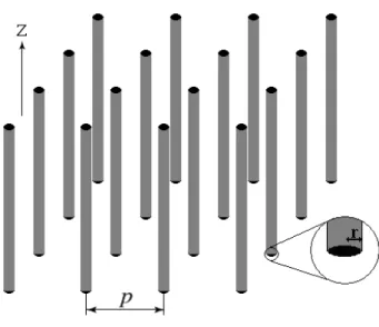
The concept of artificial dielectric materials was first introduced by Kock [12], and used in the design of low-profile dielectric lens at microwave frequencies. An example of artificial dielectric is a wired medium, Fig. 2.6, which was introduced in the 1950s. The permittivity in a medium of wires that has a frequency dependence of the plasma type frequency dependence that is negative below the plasma frequency but small and positive above this frequency. This structure has a negative permittivity and positive permeability.
The first real artificial metamaterial structure was designed and experimentally demonstrated by Smith [13]. This structure was inspired by the work of Pendry [14] who introduced the structure shown in Fig. 2.7b. This structure like the wired medium can be designed to have a plasmatic type frequency dependence in the microwave range. This structure has a negative permeability and positive permittivity.
Fig. 2.6 – The geometry of wire medium: a lattice of parallel conducting thin wires.
Fig. 2.7 – Metamaterials constructed with common dielectrics and metals: (a) negative permittivity and positive permeability, (b) negative permeability and positive permittivity, and (c) double negative media DNG [15].
In the structure shown in Fig. 2.7a if the excitation electric field E is parallel to the axis of the wires E z we have from [15]:
ε ω 1 1 j (2.27)
where ω 2πc / p ln p/r (c: speed of light) is the electric plasma frequency, and ζ ε pω /r /πσ (σ: conductivity of the metal) is the damping factor due to metal losses. From [15] we have that:
Re ε 0, for ω ω ζ (2.28)
if ζ 0 from [15] we have,
ε 0 for ω ω . (2.29)
The permeability is µ , since there is no magnetic material present (µ 1). The structure shown in Fig. 2.7b if the excitation magnetic field H is perpendicular to the plane of the rings H y from [15],
µ ω 1 F 1 F j F (2.30)
where F π r/p , ω c
/ is a magnetic resonance frequency, and ζ 2pR (R :
metal resistance per unit length) is the damping factor due to metal losses. From [15] Equation 2.30 reveals that a frequency range can exist in which Re µ 0 in general
ζ 0 . In the lossless case ζ 0 , it appears that [15],
µ 0, for ω √ F ω (2.31)
An essential difference between the plasmonic expressions for ε and µ is that the latter is of resonant nature µ ω ω ∞ , whereas the former is a non-resonant expression. The resonance of the structure is due to the resonance of its SRRs, given in [15] by ω 3pc / π ln 2d/s r .
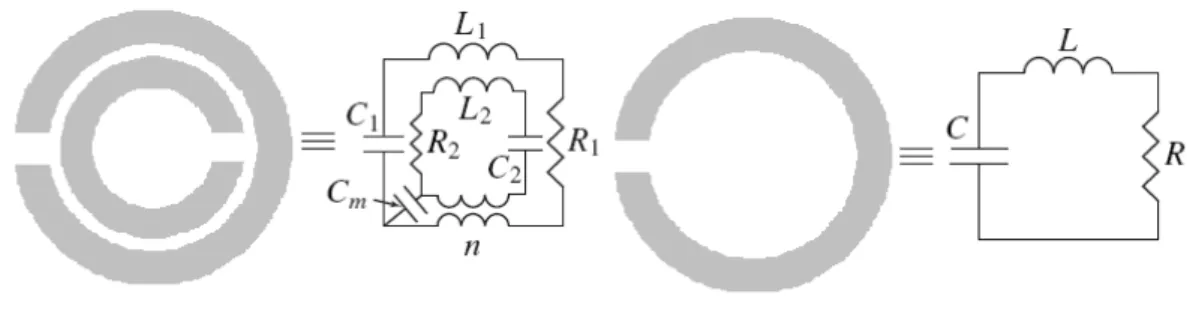
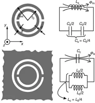
The pair of concentric rings shown (Fig. 2.7b) is an artificial magnetic material formed by resonant metallic elements. This structure is called Split Ring Resonator (SRR) and due to the small gap between the rings the structure has a larger resonant wavelength then the diameter of the rings. This small space also produces high capacitive values, which reduce the value of the resonance frequency. A magnetic flux penetrating the rings induces a current in the rings that will produce its own current flow that increases or is oppose to the incident field. It results in low radiative losses and in the high value of quality factor. At frequencies below the resonance frequency the real part of the permittivity becomes positive and at frequencies above the resonance becomes negative. This negative permeability along with the negative permittivity of the wire allows the construction of a metamaterial structure shown in Fig. 2.7c.
The equivalent circuit of a SRR is shown in Fig 2.8 [15]. In the double ring configuration (left), capacitive coupling and inductive coupling between the larger and smaller rings are modeled by a coupling capacitance (Cm) and by a transformer (transforming ratio n), respectively. In the single ring configuration (right), the circuit model is that of the simplest RLC resonator with resonant frequency ω 1/√LC. The double SRR is essentially equivalent to the single SRR if mutual coupling is weak, because the dimensions of the two rings are very close to each other, so that L1 ≈ L2 ≈ L and C1 ≈ C2 ≈ C, resulting in a combined resonance frequency close to that of the single SRR with same dimensions but with a larger magnetic moment due to higher current density.
The split-ring resonators are widely used since they can be manufactured using printed circuit technology. The artificial magnetic material with frequency-dependent positive permeability has also been build by using double circular ring resonators. A split-ring resonators, exhibits negative permeability within a certain frequency band near the resonant frequency of the single split-ring resonator. Theoretical results for the permeability using a thin wire and permittivity using a SRR are shown in Fig. 2.9, the results were obtained from equations 2.27 and 2.30, the substrate material is considered vacuum and a Perfectly Electrically Conducting (PEC) as the material for the CSRR.
(a)
(b)
2.4 Bianisotropic Media
Considering the Maxwell’s theory of macroscopic electromagnetism, material media are described phenomenologically by constitutive relations. Depending on the particular form of the constitutive relations, a medium can be characterized as linear or nonlinear; conducting or non-conducting; dispersive or non-dispersive; homogeneous or inhomogeneous; isotropic, anisotropic, or bianisotropic. An isotropic medium is characterized by a scalar permittivity that relates D to E, and by a permeability that relates H to B. In an anisotropic medium, either or both of the permittivity and the permeability can assume the form of a three-dimensional tensor. The constitutive relations of a bianisotropic medium relates D to both E and B, and H to both E and B. Similarly to the anisotropic case, their relationships are provided by three-dimensional tensors [16]. When all four tensors become scalar quantities, the medium may be called bi-isotropic. Just like an isotropic medium or an anisotropic medium, which provides a phenomenological description of many physical media, a bianisotropic medium can also be realized by a large class of material [16].
An explanation of this fact is the bianisotropic which is associated with the simultaneous presence of both anisotropic and magnetoelectric behavior, e.g. particles chiral and omega shown in Fig. 210. The insulation behavior can not be described in terms of permittivity and permeability due to the electromagnetic coupling effects between the sets of inclusions that affect their performance, as a result the electric field not only induces electric polarization, but also magnetic. The same is true for the magnetic field, materials that have this characteristic are called bianisotropic [1].
Fig. 2.10 – Bianisotropic particles: (a) chiral, (b) omega, and (c) double chiral.
The bianisotropic medium is the most general type of material that can be described in terms of normal material parameters. They have been used in many applications, such as the design of radar absorbing materials for stealth technology and polarization transformers.
These bianisotropic materials are anisotropic and can be characterized by uniaxial permittivity and permeability tensors [18].
ε ε ε 0 0 0 ε 0 0 0 ε (2.32) µ µ µ 0 0 0 µ 0 0 0 µ (2.33)
2.4.1 Double-Negative and Indefinite Media
A material will be denoted throughout as a double positive (DPS) medium if its relative permittivity ε ε/ε and permeability µ µ/µ are both positive. On the other hand, the relative permittivity and permeability are both negative in a double negative (DNG) medium [6].
The DNG media, materials with both negative permittivity and permeability, have become almost synonymous with metamaterials. One way to build a uniaxial DNG is to use the structure described in Fig. 2.7c that was suggested by Pendry [13]. This structure can be seen in Fig. 2.11 in three-dimensional form, where the arrangement of wires allows the realization of negative permittivity and the network of SRR the negative permeability.
2.4.2 Photonic and Electromagnetic Band Gaps
The electromagnetic crystals, or photonic crystals, when operating at optical frequencies are often termed electromagnetic band-gap (EBG) or photonic band-gap (PBG) materials. These crystals are structures composed of electromagnetic periodic dielectric or metallo-dielectric, operating at wavelengths that are comparable to the period, and one of its characteristics is that they have passbands and stopbands, which affect the propagation of electromagnetic waves [1].
Basically, these crystals contain regularly repeating internal regions of high and low dielectric constant. Electrons or photons behaving as waves, propagate, or not, through this structure depending on their wavelength. Wavelengths that are allowed to travel are known as modes, and groups of allowed modes form bands. Disallowed bands of wavelengths are called electromagnetic or photonic band gaps.
Moreover, these PBG or EBG occur in natural biological systems, for example the color generating nanoarchitectures in the cover scales of the Morpho butterflies that use multiple layers of cuticle and air to produce striking blue color, as shown in Fig. 2.12.
Courtesy of Prof. Dr. Dacio Rocha Brito from Universidade Estadual de Alagoas Fig. 2.12 – The blue-green color on several species of butterflies is caused by the nanoscale structure of the
insects’ wings.
The first studies and demonstration of a photonic crystal with a complete bandgap, see Fig. 2.13, were carried out in the early 1990s [19]. Since then, photonic and electromagnetic crystals have found numerous applications in FSSs and as components for waveguide and resonators, both in optical and microwave regimes.
Fig. 2.13 – The first photonic crystal with a complete band gap [19].
Electromagnetic crystals are also classified as electromagnetic bandgap structures and high-impedance surfaces at microwave frequencies. Some practical applications of EBGs include antenna beam narrowing and shaping using Fabry-Perot like EBG cavity [20], mobile antenna efficiency improvement using Mushroom-like EBGs [21] amongst others. Typical HISs are thin composite layers with reflection coefficient +1, and hence, the HIS behaves as though it were a magnetic conductor. For this reason, HIS’s are also referred to as artificial magnetic conductors (AMCs). An example of a HIS application is shown in Fig. 2.14 from [22]. In this application a bowtie wideband antenna is place above a HIS substrate.
2.5 Summary
In this chapter a detailed discussion about the theoretical background of metamaterials was presented. We provided theoretical information about the components of a left-handed material, negative permittivity and negative permeability structures. We also showed that the simultaneous negative values for permittivity and permeability results in negative refraction. In this review we have stressed the novelty of electromagnetic metamaterials and shown the great flexibility that we now have to design materials with the power to control electromagnetic radiation.
Chapter 3
Frequency Selective Surfaces
This section provides the necessary Frequency Selective Surface (FSS) knowledge to understand and design these structures. The theory governing the use of FSSs has evolved directly from the diffraction grating used in optics. David Rittenhouse discovered the filtering properties of a frequency selective surface in 1786 [23], He noted that some colors of a light spectrum are suppressed when he observed a lamp through a silk scarf. Due to the simplicity of the filtering process achieved by these structures, they are used in many areas of engineering. This simplicity is the reason why the FSSs receive great attention in many areas of electromagnetic.
Frequency Selective surfaces are planar periodic structures that behave like inductance and capacitance towards incident waves and hence behave as spatial filters to electromagnetic energy. The surface is assembled with identical patch or aperture conducting elements repeating periodically in either a one or two-dimensional array [24-26]. Frequency selective surfaces can be fabricated as planar 2-dimensional periodic arrays of metallic elements with specific geometrical shapes, or can be periodic apertures in a metallic screen. The transmission and reflection coefficients for these surfaces are dependent on the frequency of operation and may also depend on the polarization and the angle of incidence. The versatility of these structures are shown when having frequency bands at which a given FSS is completely opaque (stop-bands) and other bands at which the same surface allows wave transmission [24].
In optics spatial filter is a beam converging device coupled with a filter that uses the principles of Fourier optics to alter the structure of a beam of coherent light or other electromagnetic radiation. The filter is used to remove interference patterns in the output of a laser beam. In spatial filtering, a lens is used to focus the beam. Because of diffraction, a beam that is not a perfect plane wave will not focus to a single spot, but rather will produce a
pattern of light and dark regions in the focal plane. The interference is removed from the beam in the following manner the laser output appears as a point source at infinity and the interference producing sources are at finite distance from the filter, due to the difference in the point of origin, focusing the beam will produce an image of the source with all the interference defocused in an annulus around the focused beam at the filter. The focused beam will pass through the filter and the interference will be severely attenuated.
To understand the concept of spatial filtering, consider an incident wave striking a metal surface as shown in Fig. 3.1. Imagine a single electron in the surface plane with a direction vector perpendicular to the plane. The E-vector of the incident wave is parallel to the metallic surface. Therefore, when the incident wave strikes the metal surface, it exerts a force on the electron causing it to accelerate in the direction of E-vector. In order to keep the electron in a continuous oscillating state, some portion of energy must therefore be converted into the kinetic energy of the electron. This will result in the absorption of most of the incident energy by the electron and its reflection by the electron aceleration (Low Transmittance). The transmission through the filter will be zero if all the energy of incident wave is converted to the kinetic energy for the electron.
3.1 – Electron in the plane oscillates due to the force exerted by incident wave resulting in low transmittance.
Referring to Fig. 3.2, in which the direction vector of the electron is perpendicular to the E-vector of incident wave. In this case, despite of force exerted by the E-vector, the electron is constrained to move along the direction vector. Hence the electron is unable to absorb the kinetic energy of incident wave. Therefore, the wave is not absorbed and a high transmittance occurs.
3.1 FSS Elements
A periodic surface is basically a set of identical elements arranged in a two-dimensional or infinite arrays. Considering the structure shown in Fig. 3.3. The incident field E is given by [25],
E ue , for z 0 (3.1)
where the time factor exp jωt has been suppressed, and k 2π/λ ω/c is the wave number. The unitary vector u satisfies the relation · 1 and · 0. It defines the polarization of the incident field, e.g., u for a linearly polarized field, and u
x jy /√2 for a circularly polarized field [25].
Fig. 3.3 – Metal screen illuminated by a normally incident plane wave [1].
This frequency selective property described by Rittenhouse proved the fact that surfaces can exhibit different transmission properties for different frequencies of incident wave. Hence, such surfaces are now called frequency selective surfaces (FSSs). As mentioned before an FSS can be considered as a free-space filter, which could be used to pass certain
frequencies and stop others. Therefore, an FSS either blocks or passes waves of certain frequencies in free space [27]. A FSS comprises a bi-dimensional periodic array of elements patches or apertures in a conducting screen, which must be either freestanding or etched on supporting dielectric substrates. Based on the element geometry, FSSs can be classified into two categories as shown in Fig. 3.4 [24].
Fig. 3.4 – Basic FSS geometries: The patch-array produces a capacitive response, whereas the array of slots is inductive.
The main difference between this two cases is that we excite electric currents on the squares while we excite "magnetic currents” in the slot square case (i.e., there is a voltage distribution in the slots). The two cases become quite similar and symmetric if we compare the electric field in the square case and the magnetic field in the slot square case. Following this principle a Frequency Selective Surface is a periodic array of either radiating or non-radiating elements or slots, which effectively act as a band stop or band, pass filter respectively to electromagnetic waves. There are a wide variety of possible elements, which can be used to realize FSS arrays.
3.2 Different FSS Element Types
As mentioned before FSSs can be seen as electromagnetic filters that are normally realized using periodic structures formed by arrays of conducting elements on a dielectric substrate or by periodic aperture elements in a conducting sheet.
The basic types of frequency selective surfaces elements are: center linked or N-pole, type of loop, interior solid or plate type and combinations of the others elements. Fig. 3.6 shows examples of FSSs elements [25].
Fig 3.5 – The four major groups of FSS elements. These elements may be used to construct band stop filter type FSS arrays. Elements are ordered from most narrowbanded on the left to most wide-banded on the right [25].
3.2.1 Infinite FSS Arrays
Considering the periodicity a true frequency selective surface is infinite. Thus, the concept of starting to discuss the properties of infinite arrays and apply that knowledge for a finite array design as in practice [24].
3.2.2 Finite FSS Array
Although only finite ones can be fabricated, the infinite FSS periodical structures are useful to identify many of its properties. Two main considerations must be made in the design of a finite array, i.e., edge diffraction and surface waves radiating. The edge diffraction causes the stopband bandwidth to rise. Surface waves appear about 20-30 per cent below the resonance, when the spacing between elements is less than 0.5λ [25]. Surface waves can be a problem when using FSSs.
The electromagnetic band-gap structures have been employed in different applications to reduce the effects of surface wave. An example is the use of a high impedance surface, a
metamaterial with dispersive permeability on top of a FSS array. The HIS has a high-impedance frequency regime and the surface wave suppression in the high high-impedance band gap is a consequence of the FSS connected to its ground plane using a metallic via.
3.3 Metamaterial FSSs
The most common FSSs types take the form of planar, periodic metal or dielectric arrays in 2D space. Frequency behavior of an FSS is determined by the geometry of the surface unit cell provided that the surface size is infinite. As mentioned before FSSs were originally introduced as spatial filters and since that they have been employed in a variety of other applications including most recently metamaterial applications.
Metamaterial frequency selective surfaces can be used in designing reactive impedance surfaces in a form of an artificial magnetic conductor (AMC) and electromagnetic band-gap (EBG). The FSS are an alternative to fixed frequency metamaterial where static geometry and spacing of unit cells to determine its frequency response. FSSs have reflective characteristics with a certain phase and amplitude that allow frequency changes in a single medium and are not restricted to a fixed frequency response.
The classic example of AMC is the high impedance surface described in [33]. This high impedance surface is a periodic array printed in a dielectric substrate where each element of the array is connected to the ground plane. This array is called mushroom. In a normal electric conductor electric current flow is allowed, in an AMC currents will not be allowed to travel through the medium, which in turn bans the propagation of surface waves inside the substrate.
This metamaterial FSS will be used as a ground plane for antennas in order to effectively suppress undesirable wave fluctuations, i.e., surface waves inside the substrate, while producing good radiation patterns. The type of high impedance surface used in this work is show in Fig. 3.6. The square metal patches are raised above the surface, and points at the center are the vias of vertical connection.
Fig. 3.6 – A transver impedan field, Et cannot b properti impedan used in impedan Fig. 3.7 – – Superior view cylinders. An AMC c rse wave im nce is defin t/Ht. In this bear a tang ies can the nce transfor n design o nce, Fig. 3.7 – A corrugated w of a high im can be seen mpedance a ned as the ra case an inf gential magn explained rmer, a shor f corrugate 7. d reactive surf mpedance surf n as a surf at the surfac atio of the t finite imped netic field a by the tra rt impedanc ed surfaces face acting as face, patches c face with i ce is infinit transverse e dance corres and hence t ansmission ce is transfo s behaving an AMC. connected to t ncreased su te (for an in electric field sponds to H the name m line theory ormed to an as an ope
the ground pla
urface impe ncident plan d over the t Ht ≈ 0, mean magnetic co y. Consideri n open impe en circuit
ane with meta
edance. Ide ne). The tra transverse m ning that the
nductor. Th ing a quart edance. Thi in terms o l eally the ansverse magnetic e surface he AMC ter-wave is idea is of wave
The HIS can be viewed as a network of parallel LC resonant circuits, which acts as a 2D electric filter to block the flow of currents and consequently suppresses the surface waves along the sheet. When the patches are connected to the ground plane its impedance changes and the surface waves properties are altered. The HIS equivalent LC circuit from [33] is shown in Fig. 3.8. The capacitance occurs due to the proximity of the top metal patches, while the inductance originates from current loops within the structure. In the LC resonance frequency the surface impedance is high and an electromagnetic band gap is formed so waves are not bound to the surface and they radiate into surrounding areas.
Fig. 3.8 – Origin of the equivalent circuit elements left and equivalent circuit model for the high-impedance surface right [33].
3.4 Antenna Bandwidth Augmentation
Frequency selective surfaces can be used as a superstrate to enhance the performance of a number of antennas [34-36]. These superstrates offer the advantage of ease of fabrication with microstrip technology and reduced thickness as compared with those of the dielectric type superstrates. The FSS can suppress its grating lobes and as a result a high gain antenna can be obtained.
Another way to achieve a broader bandwidth is the use of a Fabry-Pérot (FP) [37-42] configuration. Antenna applications that require high directivity need the use of array designs with complex feed network to comply with the directivity specifications using conventional technology. A FP configuration uses a single radiating element instead of a array that can simplify considerably the complexity of receivers and transmitters, reducing the size and the mass of the conventional configurations. The FP medium consists of a capacitive-type frequency selective surface array that is used as superstrate and an artificial magnetic conductor as ground plane. The realized gain and the bandwidth of the antenna can be simultaneously improved by using the tapered artificial magnetic conductor. As a result the
maximum gain is increased and the bandwidth is improved when compared to the single uniform antenna. In Chapter 6 this phenomenon will be described.
3.5 Summary
This chapter has presented a historic background and a review of literature on FSSs. Particular emphasis has been placed on factors, which influence the FSS response, including the element geometry, the element conductivities, the dielectric loading, and the signal incident angles. Studies have indicated that the fundamental frequency characteristics of an FSS are mainly governed by the element geometry, including element dimensions and shapes. With a proper choice of element dimensions and shapes, an FSS could, to some extent, be insensitive to incident angles and signal polarizations. Some metamaterial like FSSs were also described.
Chapter 4
Planar Antennas and Microstrip Filters
with CSRR Parasitic Structures
Interference is a big issue for UWB communication systems. Since the UWB spectrum is so large (3.1-10.6 GHz) the entire U-NII (Unlicensed National Information Infrastructure) band (5.15-5.825 GHz) overlaps with its spectrum. Fig. 4.1 shows the U-NII spectrum inserted in the UWB spectrum. As UWB transmitters must not cause electromagnetic interference on any nearby communication systems, a solution to notch this band is needed. In this chapter two solutions to achieve a band notched function are presented.
Fig. 4.1 – Ultra wideband and UN-II spectrums.
As a first solution, a parasite metamaterial structure is inserted directly in the antennas patch. Many UWB antennas designers have been working on several alternative solutions to achieve band rejected function. Some of the approaches proposed in literature are embedding
slots (arc-slot) [43], double U-slots [44], stubs or spurlines [45], square-slot [46], V-slot [47], and attaching bar [48]. In these classical solutions the band-notched characteristic comes with many problems mainly due to the difficulty in controlling the band-notch width in a limited space. Some designs occupy wider band-notch (more than 2 GHz) or have only single band- notched characteristic. The solution proposed in this work to block this band was found by introducing a metamaterials SRR structure in the antenna’s patch for notching the entire U-NII band. As mentioned before, a SRR is a pair of concentric annular rings splited at opposite ends. There are two types of SRR: one were the rings are made of metal like copper and the other is a slot-type SRR where the rings are slots on a nonmagnetic metal, which are etched in the foursquare patch. These structures are also called Complementary Split Ring Resonator (CSRR) where both rings have small gap between them. Different from classical solutions the band-notch of the CSRR can be easily tunable by changing is dimensions and also have a tunable dual band-notched characteristic.
The second solution is a microstrip UWB filter with the same goal as the first solution, i.e., notch the UN-II band. There are many classical methods for designing such filters some examples are the stepped-impedance resonator (SIR) [49], the spurline [50], and the defect ground-structure [50]. The filter solutions proposed in this work consist of a simple microstrip line backed by the CSRR placed on its ground plane. This structure present, many advantages like a tunable band-notch by simple changing its physical dimensions, band-notch augmentation by increasing the number of CSRRs in the ground plane and easy design and fabrication when compared to some classic solutions
The CSRR-based medium has the property of negative effective permittivity and can be used to reject unwanted frequency band. Due to the relatively high insertion loss for CSRR slots, the CSRR has a band-stop filtering property. Moreover, the band-notched frequencies can be varied by adjusting the length of C-shaped slot and the dimensions of CSRR independently. Simulated and measured results of the proposed prototypes are provided.
4.1 – Ultra Wideband Monopole Antenna with Split Ring
Resonator as Filter
In the last years a special attention has been devoted to the development of Ultra Wideband (UWB) monopole antennas [51 - 53]. The UWB is a short-range wireless technology for transmitting large amounts of data at very high-speed with very low power,
generally the effective isotropic radiated power (EIRP) is -41.3 dBm/MHz. The bandwidth of the UWB signal is at least 25% of the center frequency, and the unlicensed use of UWB is in the range of 3.1 to 10.6 GHz [54]. The use of UWB systems needs efficient antennas to provide acceptable bandwidth requirements, and radiation pattern characteristics throughout the designated UWB spectrum. It is generally accepted that for antennas to be classified as ultra-wideband, the requirement will be to satisfy minimum fractional bandwidths of at least 20 % or 500 MHz or more [55].
There are many theories to explain the operation of UWB antennas. In the 1950s Rumsey’s principle [56] was introduced to explain a family of that he called frequency-independent antennas. This principle suggests that the impedance and pattern properties of an antenna will be frequency independent if the antenna shape is specified only in terms of angles. To satisfy the equal-angle requirement, the antenna configuration needs to be infinite in principle, but is usually truncated in size in practice. This requirement makes frequency-independent antennas quite large in terms of wavelength. It has been verified that for spiral antennas, conic spiral antennas and some log-periodic antennas the principle can be applied.
The Rumsey’s principle was, probably, inspired by Mushiake and Uda work in the 1940s on the constant independent of self-complementary antennas for all frequencies, half the intrinsic impedance of free space [57], which were invented by Runge in the 1930s [58]. They discovered that the product of input impedances of a planar electric current antenna (plate) and its corresponding ‘magnetic current’ antenna (slot) was a real constant. Therefore, an antenna built in a complementary structure of electric and magnetic currents exhibits a real constant impedance. This theory, referred as ‘Mushiake’s relation’, has led to the development of a large family of self-complementary antennas with constant input impedance. Mushiake’s relation has relaxed the condition for achieving ultra wide impedance bandwidth. However, it doesn’t guarantee constant radiation patterns over the operation bandwidth [55]. Incidentally, an infinitely long biconic antenna was also demonstrated to exhibit constant impedance, although it is not a self-complementary structure.
Lately, many researchers have started to look into UWB with the development of the latest communication systems, and a surge of research interest into small UWB antennas has been raised. Such antennas have to be small enough to be compatible to the UWB unit and omnidirectional radiation patterns are often required for UWB terminal antennas. Finally, a good time-domain characteristic, i.e., a good impulse response with minimal distortion is also required for transmitting and receiving antennas. For these tasks two families of compact antennas have emerged to provide solutions. The first family is originated from biconal
antennas, but in a compact planar configuration, such as bowtie, diamond, circular and elliptical disc dipoles. They provide UWB characteristics and also satisfy other requirements imposed by commercial UWB systems. The second family is due to further developments on broadband monopole antennas, in which planar elements, such as circular, square, elliptical, pentagonal and hexagonal discs appear.
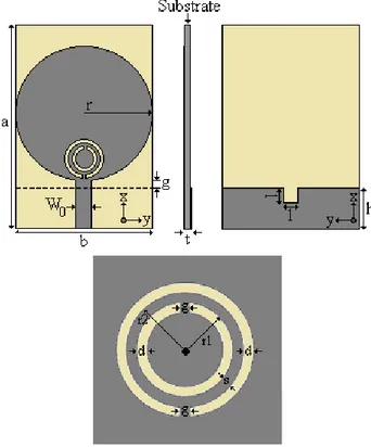
For this investigation, a circular monopole antenna was chosen as a starting point. A monopole antenna is a type of radio antenna formed by replacing one half of a dipole antenna with a ground plane at right angles to the remaining half. If the ground plane is large enough, the monopole behaves like a dipole, as the reflection in the ground plane behave as the missing half of the dipole, except that the radiation from the reflected half is added to that of the real half (see image antenna). However, a monopole will have a directive gain of 5.19 dB (gain is twice, 3 dB over) that for a half-wave dipole antenna, and a lower input resistance [50]. In general, these antennas are built into microstrip structures with limited ground plane, in the monopole form. For this reason, they have small dimensions and weight, and easy construction, which are some of its main advantages. The geometry of the antenna considered as a starting point is shown in Fig. 4.2 [65].
Fig. 4.2 – Circular monopole antenna, the gray region denotes a conductor material.
The self-resonant antenna consists of a circular monopole disc with a radius “r” and is fed by a 50Ω microstrip line, printed on a dielectric substrate with dimensions “a-b” and thickness “t”, backed by a ground plane of height “h”. The feeding line width is represented by W0 and “g” is the gap between the disc and the ground plane. The structure shown above was considered to start the experimental research implementation, performed with the construction and measurement, while the Computer Simulation Technology: Microwave Studio (CST MWSTM) was used as an auxiliary tool in the simulation process. The simulated
return loss (S11) and Smith Chart results for this monopole antenna are shown in Fig. 4.3. In the computer aid simulation an Arlon DiClad 880TM substrate with coppered plates on both sides was used. The thickness of the dielectric layer, “t” is 0.768 mm, the inherent dissipation of electromagnetic energy (dielectric loss tangent) is 0.0009, the permeability is 1, and the permittivity εr is 2.17. Once the antenna was adapted the following dimensions were determined (see Fig. 5.1) a = 30 mm, b = 20 mm, r = 10 mm, h = 6 mm, g = 1 mm, W0 = 2.4 mm.
(a)
(b)
The bandwidth is recommended to guarantee an S11 of –10dB over the frequency band of interest and Fig. 4.3 (a) show that the antenna has a large bandwidth, i.e. the S11 is below −10 dB in the extension from 3.7 GHz to 8.2 GHz. The antenna has also a good matching to the 50Ω microstrip line. To optimize the antenna for a bandwidth augmentation the ground plane is truncated with a rectangular cut introduction of width “l”, which consists in reducing the capacitance in the microstrip line connection region with the circular conductor patch, to improve the impedance matching. Fig. 4.4 shows the improved design.
Fig. 4.4 – Circular monopole antenna with improved ground plane, where the gray region denotes a conductor material.
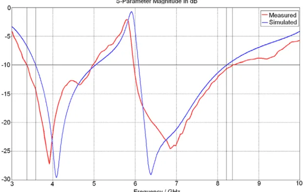
The return loss for the improved antenna is shown in Fig. 4.5. The new design has the same dimensions as the first one and the rectangular cut has the width l = 2.4 mm which is equal to the microstrip feeding line W0. It can be seen that with the rectangular cut introduction the bandwidth is increased by about 17%, in the improved bandwidth the S11 is below −10 dB form 3.8 GHz to 8.9 GHz.
Based on the obtained results it can be said that, according to the antenna theory [59], the maximum available power Wm of a receiving antenna for a matched load is proportional to the product of λ2, |E|2, and D.
Wm: Maximum available power of receiving antenna with a matched load. λ: Wavelength.
: Electric field.
D : Directivity (Directive gain) of the receiving antenna.
The received power “Wm” decreases to smaller values with increasing frequencies in inverse proportion to the square of the frequency when its directivity “D” remains unchanged [60]. The term frequency-independent is reserved for antennas that have no theoretical limitation on the bandwidth of operation. Such a property is really unimaginable from its nomenclature. In Practice, however, the performance cannot be even approximately constant for all frequencies. There are physical bounds that limit the band over which the performance can be held almost constant.
4.1.1 –
Complementary Split Ring Resonator StructureThe SRR was first introduced in [61] as a new method for the design of metamaterials structures. If the excitation magnetic field H is perpendicular to the plane of the rings H y , so as to induce resonating currents in the loop and generate equivalent magnetic dipole moments. This metamaterial exhibits a plasmonic-type permeability frequency function that in the lossless case it appears that [61],
µr < 0 (4.1)
This investigation was carried out considering a CSRR structure and its stop band characteristics. A SRR can be mainly considered as a resonant magnetic dipole, with very high Q, that can be excited by an axial magnetic field, while the CSRR essentially behaves as an electric dipole (with the same frequency of resonance) that can be excited by an axial electric field [62]. As mentioned in Chapter 2 the SRRs behave as an LC resonator that can be excited by an external magnetic flux, exhibiting a strong diamagnetism above their first resonance. The SRRs also exhibit cross-polarization effects, so that excitation by a properly