O
pen
A
rchive
T
OULOUSE
A
rchive
O
uverte (
OATAO
)
OATAO is an open access repository that collects the work of Toulouse researchers and
makes it freely available over the web where possible.
This is an author-deposited version published in :
http://oatao.univ-toulouse.fr/
Eprints ID : 11403
To link to this article : DOI:10.1109/TNS.2013.2249095
URL :
http://dx.doi.org/10.1109/TNS.2013.2249095
To cite this version :
Gaillardin, Marc and Girard, Sylvain and
Paillet, Philippe and Leray, Jean-Luc and Goiffon, Vincent and
Magnan, Pierre and Marcandella, Claude and Martinez, Martial and
Raine, Mélanie and Duhamel, Olivier and Richard, Nicolas and
Andrieu, F. and Barraud, S. and Faynot, O. Investigations on the
vulnerability of advanced CMOS technologies to MGy dose
environments. (2013) IEEE Transactions on Nuclear Science, 60 (4).
pp. 2590-2597. ISSN 0018-9499
Any correspondance concerning this service should be sent to the repository
administrator:
[email protected]
Investigations on the Vulnerability of Advanced
CMOS Technologies to MGy Dose Environments
M. Gaillardin, Member, IEEE, S. Girard, Senior Member, IEEE, P. Paillet, Senior Member, IEEE,
J. L. Leray, Fellow, IEEE, V. Goiffon, Member, IEEE, P. Magnan, Member, IEEE, C. Marcandella, M. Martinez,
M. Raine, Member, IEEE, O. Duhamel, N. Richard, F. Andrieu, S. Barraud, and O. Faynot, Member, IEEE
Abstract—This paper investigates the TID sensitivity of
silicon-based technologies at several MGy irradiation doses to evaluate their potential for high TID-hardened circuits. Such circuits will be used in several specific applications suc as safety systems of current or future nuclear power plants considering various radiation en-vironments including normal and accidental operating conditions, high energy physics instruments, fusion experiments or deep space missions. Various device designs implemented in well established bulk silicon and Partially Depleted SOI technologies are studied here up to 3 MGy. Furthermore, new insights are given on the vul-nerability of more advanced technologies including planar Fully Depleted SOI and multiple-gate SOI transistors at such high dose. Potential of tested technologies are compared and discussed for stand-alone integrated circuits.
Index Terms—Bulk silicon, FinFET, fully depleted, MGy
irradi-ation, multiple-gate transistors, nanowire, partially depleted, SOI, TID.
I. INTRODUCTION
I
NCREASING needs for high-TID tolerant electronic sys-tems have been revealed recently for several applications including high energy physics instruments, fusion experiments or deep space missions such as jovian missions. Futhermore, in March 2011, the Fukushima Daichii event revealed the need for enhanced radiation tolerance of electronic systems, both for use in future nuclear facilities and for the new security systems to be implemented in existing nuclear power plants, spent-fuel pools of future facilities. Higher radiation tolerance appears manda-tory to ensure the functionality of equipments including elec-tronic components in the case of an accident occurring within the nuclear facility; this would induce a strong and rapid in-crease of radiations at levels largely exceeding the ones consid-ered for normal operating conditions. The consideration of ac-cident constraints strongly increases the needed Total Ionizing Dose (TID) tolerance for different electronic technologies. Offcourse, radiative constraints and other environmental conditions like temperature, pressure and chemical hazards depend on the accident scenario as well as on the location of the considered device inside the installation. To the best of our knowledge, the most constraining scenarii are associated with TID in the order of few MGy deposited in few weeks at the device level. In these cases, in addition to increased radiative constraints, other environment parameters will change during the accident phase which may also affect the device, such as the temperature and pressure that could increase up to 160 and 560 kPa [1], [2]. Usually, accident simulation tests to qualify containment in-strumentation or control cables include a gamma radiation ex-posure, which represents the total accident and post-accident ir-radiation dose, followed by a thermodynamic test in steam and under pressure to fully characterize the impact of the harsh en-vironment on the device functionality [1].
TID effects on Commercial Off-The-Shelf (COTS) micro-electronics devices have been widely studied up to 10 kGy, showing that most COTS components survive to doses of at least 5 Gy [3] without any radiation hardening effort. Some COTS devices can withstand doses exceeding this value, but in this case, radiation tests are necessary to identify the maximal dose before the component loses its functionality. The 5 Gy to 10 kGy dose range covers most of the considered applications in space [4], avionics or terrestrial environments [5] but is not representative of the larger TID considered in the harsh environ-ments considered in this study. This is particularly true for the case for future nuclear facilities but also for deep space missions for which high TID are considered. The TID induced degrada-tion is mainly linked to the generadegrada-tion of electron–hole pairs within the metal-oxide semiconductor (MOS) structure that can be trapped at point defects and result in a shift of the oper-ating conditions of the device. The amplitudes of these radia-tion effects have been shown to depend on device parameters such as geometry, design and biasing conditions. Furthermore, the impact of these changes depends on the device profile of use; we could consider that for doses exceeding 10 kGy, only few COTS radiation tolerant components survive without ap-plying hardening techniques. Radiation-hardened by design or radiation-hardened by technology devices can be developed, as demonstrated by the researchers involved in the Large Hadron Collider (LHC) instrumentation design [6]. Among the different current technologies, bulk CMOS technology appears as the most promising to resist to high TID levels. However, up to now, the TID response of recent advanced CMOS technologies, like Silicon-On-Insulator (SOI) or FinFET is not documented at MGy dose levels.
The goal of this paper is not to qualify specific devices or technologies for high TID environments but to highlight the possible potential of current and advanced technologies for in-tegration in nuclear facilities. We investigate the intrinsic vul-nerability of current (Bulk, Partially-Depleted (PD) SOI) and advanced (Fully-Depleted (FD) SOI, Multiple Gate Devices) CMOS technologies to withstand high TID levels (up to 3 MGy) since to the best of the authors’ knowledge, no data exist on the high TID sensitivity of advanced CMOS technologies such as planar FDSOI and SOI FinFETs. For this preliminary study, we consider 3 MGy as a sufficiently large dose to cover the radiative constraints for both ageing effect (cumulative effects of the en-vironmental conditions corresponding to normal operation [7]), accident and post-accident effects.
For each technology, we characterize the impact of geometry, design and biasing conditions on the TID response. CMOS cir-cuits exposed with no bias (all terminal grounded or floating) generally exhibit a considerably lower degradation than their biased counterparts. Then, we characterize the device response under bias to provide the worst-case response. We also evaluate the radiation sensitivities of these technologies unbiased since only most electronic systems may be shut down most of time during a deep space mission or in the case of a nuclear accident, some electronic-based systems, may be activated after they re-ceived an important cumulated dose in their stand-by mode, to authorize the functionally-limited but crucial radioprotection or security systems in such an event.
II. EXPERIMENTALDETAILS
A. Test Procedure
On the one hand, for applications like temperature or pres-sure sensing in nuclear power plants, the surrounding environ-ment remains dominated by gamma rays leading to Total Ion-izing Doses (TID) which may reach up to few MGy (normal or accident) [8], [9]. At certain locations, neutrons of a wide energy range may also complete the radiation environment. In nuclear accidental conditions, additional betas (fuel, radioactive decay, fission products) are also expected but radiation-induced effects can arise only from penetrating radiation involving gammas and neutrons. Such effects could have potential implications for the reliability of electronic components in nuclear accidental condi-tions. On the other hand, for radiative environment encountered in deep space missions, Single-Event Effects must be consid-ered in addition to high TID. Since this paper is only focused on irradiation effects (TID); neutron-induced degradations in electronic devices and ICs will be completely overviewed in a dedicated publication. The present paper is thus focused on high TID effects on advanced CMOS technologies designed for low power purpose. To do so, we perform radiation tests at a constant dose rate of 80 (8 ) up to 3 MGy (300 Mrad) using a 10 keV X-ray laboratory source on elementary devices made of MOS transistors from various technologies. In all the following, the standard unit Gy will be used because of the high TID discussed in that paper. Devices are tested at room temperature either at wafer level or mounted in standard Dual-In Line packages. In these experimental conditions devices are ei-ther biased at the nominal voltage of the technology (cf. Table I) or grounded to match the various possible operating conditions.
TABLE I
NOMINALVOLTAGE VSTECHNOLOGYUSED TOBIASDEVICESDURING
IRRADIATION
Each total dose irradiation step is followed by static electrical measurements using a setup which includes a HP4145 through a Keithley switching matrix.
Some devices are also irradiated up to about 500 kGy (50 Mrad) under -rays at Brigitte nuclear reactor facility at SCK-CEN. Devices are irradiated at a temperature of 50 . At this lo-cation the dose rate was 1.5 kGy/h. Devices are unbiased during irradiation and characterized several days after irradiation.
B. Devices
In such a context, bulk silicon devices appear as good candi-dates to survive high TID effects [6] using specific device de-sign. Except thick field oxide isolations, such as Shallow Trench Isolation, only few dielectrics are used in the front-end of bulk silicon technologies. TID effects should thus be reduced since they mainly induce damages in oxides and at semiconductor-ox-ides interfaces. Irradiations are performed on I/O transistors de-signed using a 0.18 m COTS process to confirm their function-ality after 3 MGy and to act as a basis of comparison with other available technologies. However, bulk technology would need additional hardening techniques if SEE mitigation is necessary. Silicon-On-Insulator (SOI) technology is also a promising candidate to meet the requirements of functionality in such harsh environment. This technology has already demonstrated its ability to withstand TID in the 10 kGy (Mrad) range com-bined to very low power consumption needed for stand-alone applications. SOI/SOS technologies, either with a thick or with a partially depleted active silicon layer [10]–[12], can withstand high TID levels. In this paper, a 0.13 m PDSOI technology is studied to investigate whether or not the TID induced charge trapping in the buried oxide (BOX) is an intrinsic limitation for use in MGy dose environments.
Among available advanced CMOS technologies, planar Fully Depleted (FD) SOI is a promising candidate for stand alone ap-plications, thanks to its reduced power consumption. Its TID response is not intrinsically as good as for bulk technology but may be strongly improved using various hardening techniques including either the use appropriate SOI substrates option [13], [14] (substrate removal, thin BOX with or without ground plane implants) associated to back-biasing techniques or using a re-laxed geometry [24]. Furthermore, the complete dielectric iso-lation between devices combined with the reduced active silicon volume inherent to this technology appear as clear advantages if SEE tolerance is needed.
The next step in advanced technologies will probably be 3-D device design with FinFETs and nanowires. Indeed, this specific architecture is introduced by Intel for the 22 nm node [15] to meet the requirements of the International Technology Roadmap for Semiconductors for enhanced performances and
improved power consumption. FinFET architecture has also shown its intrinsic TID tolerance up to the Mrad range using a narrow geometry [16], [17] either in SOI or bulk silicon. SOI FinFETs may thus combine number of advantages including low power consumption, TID and SEE tolerance with the use of an appropriate geometry.
These four technologies, bulk silicon, Partially Depleted (PD) SOI, Fully Depleted (FD) SOI and SOI FinFETs are studied in this paper to review their ability to operate in MGy environ-ments.
III. MGy DOSESENSITIVITY OFSi-BASEDTECHNOLOGIES
A limited number of applications need electronic systems hardened to several MGy irradiation doses. In the 1980’s, thick SOI devices and circuits made on SIMOX BOX substrate with 1.4 m gates were tested up to tenths (and hundreds) of MGy. This technology featured body tied transistor designs which in-trinsically suppress sidewall leakage currents. Devices were de-signed and qualified for use in electronic systems in such harsh environments. In the 1990’s, SOI devices and circuits made on a thick SOI technology with 0.8 m CMOS gates were quali-fied. They have been fabricated for several years to be used in inner parts of Large Hadron Collider detectors’. More recently, bulk devices were also studied for LHC. However, to the best of the authors’ knowledge, no data exist on the TID sensitivity of advanced CMOS technologies such as planar FDSOI and SOI FinFETs up to 3 MGy, which correspond to the specific oper-ating conditions previously discussed. The main goals of this paper are to discuss whether or not unintended effects appear above 1 MGy in CMOS devices and to review a wide panel of technologies that may be chosen to design highly hardened cir-cuits.
A. Bulk Technology
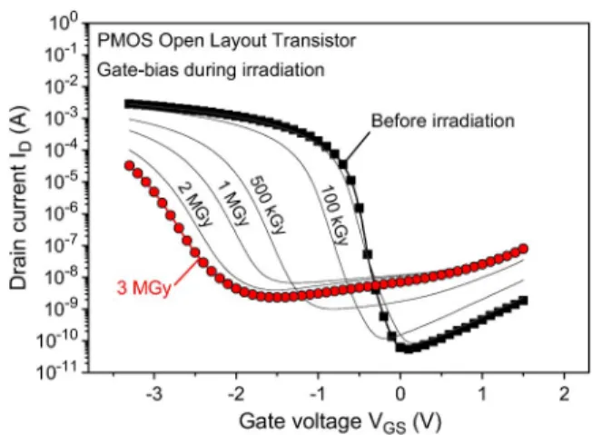
Numerous studies were dedicated to TID effects in bulk silicon technologies. They concluded that several radiation-in-duced parasitic effects may appear, including parasitic sidewall leakage current due to charge trapping in field oxides [18], threshold voltage shift due to charge trapping in gate oxides, or degradation of subthreshold characteristics due to buildup of interface traps at Si-oxide interfaces [19]. However, only few of them were focused on MGy dose environments. Faccio et al. [6] have shown that devices designed using COTS foundries can withstand doses up to 1.36 MGy. I–V measurements pre-sented in Fig. 1 on pMOS I/O transistors highlight a similar trend with a significant threshold voltage shift. Transistors de-signed using a standard open layout are highly sensitive to TID. Radiation-induced STI leakage currents and Radiation-Induced Narrow Channel Effects (RINCE) lead to limit the radiation tolerance of this technology, in both nMOS and pMOS transis-tors. In particular, Edgeless transistor designs are thus needed to ensure the functionality of bulk silicon technology at high TID. So, enclosed layout transistors (ELT) were designed to remove all parasitic field-oxide induced leakage currents. Both RINCE and parasitic sidewall leakage should then be intrinsi-cally suppressed. This is shown in Fig. 2 which presents I–V characteristics of nMOS ELT gate-biased during irradiation.
Fig. 1. Drain current vs gate voltage characteristics of bulk silicon pMOS open layout transistor with m at several TID from before irradiation (black squares) up to 3 MGy (red circles).
Fig. 2. Drain current vs gate voltage characteristics of a bulk nMOS enclosed layout transistor with m at several TID from before irradiation (black squares) up to 3 MGy (red circles).
As expected, the voltage shift associated to radiation-induced oxide trap charges is still limited to few mVs after 3 MGy. Only radiation-induced charge trapping in the thin gate oxide is involved. On the other hand, the subthreshold slope is strongly degraded due to the large buildup of interface-traps whatever the bias case used during irradiation (grounded, drain-biased or gate-drain-biased). Measurements also show that the elec-trical consumption ( : drain current at ) of ELT bulk silicon transistor does not significantly change with TID. No shoulder appears on curves displayed in Fig. 2 meaning that parasitic leakage currents are mitigated by the device design. In contrast, the drive current decreases sharply with TID, following the degradation of the subthreshold slope . This may be an issue since drive-current is a key parameter to design CMOS circuits.
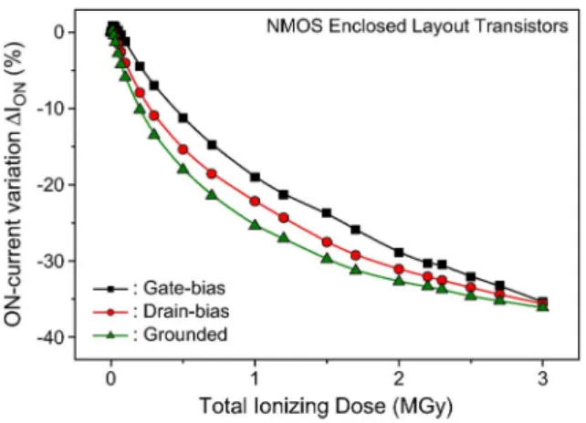
Margins should be taken into account to define reliable electronic systems operating in harsh TID environment. To do so, Fig. 3 summarizes the variation vs TID of ELT transistors biased in various conditions during irradiation: grounded, drain-biased and gate-biased. Each curve exhibits a similar shape leading to a maximum variation of 35% after 3 MGy. This value gives indications on the needed appropriate
Fig. 3. Evolution of ON-current vs TID for the bulk ELT in biased in various conditions during irradiation.
margins to design CMOS circuits hardened to MGy irradiation dose.
It is worth noting that the tested bulk devices are I/O transis-tors used to design image sensors and not core transistransis-tors of the technology. This means that their gate oxides are much thicker than in core transistors, so that they can operate with higher nominal voltages. So, core transistors from this technology will show a better TID tolerance than I/O transistors presented in this paper. One can thus consider that the high TID response of I/O transistors reported here is a worst case compared to the one re-lated to core transistors. Despite the area penalty induced by the use of enclosed layout transistor, bulk silicon technologies are promising for high TID environments, with a reduced effort of hardening by design to ensure safe operations.
B. Partially Depleted SOI Technology
SOI technology introduces an additional parasitic effect to those already reviewed in bulk silicon technologies: the radia-tion-induced charge trapping in the buried oxide (BOX). It may trigger a parasitic “back” transistor at the active silicon-BOX interface [14]. The effect has been demonstrated to depend on several parameters including geometry and bias case applied during irradiation [20]. To investigate the response of such tech-nology to high TID, irradiation tests are performed on a 0.13 m partially depleted SOI technology. All transistors are ini-tially designed using external body contacts to suppress any ra-diation-induced parasitic leakage due to charge trapping in field oxides made of STI [21], [22]. Because of the results obtained on bulk technology, only core transistors of the design kit are used for this study.
I-V curves obtained on a nMOS PDSOI transistor (cf. Fig. 4) show very limited electrical characteristic shifts. Radiation-in-duced charge trapping in the thin gate oxide has no significant effect on the threshold voltage; similarly, the buildup of inter-face-traps at the silicon-gate oxide interface induces no signif-icant subthreshold slope degradation. Only the leakage current
increases with TID.
This is due to the triggering of the parasitic back-transistor since body contacts prevent transistors from any effect of charge trapping in field oxides. The leakage current increases of
Fig. 4. Drain current vs gate voltage characteristics of a nMOS PDSOI tran-sistor with m from before irradiation (black squares) up to 3 MGy (red circles).
Fig. 5. Evolution of OFF-current (in log scale) vs TID for 0.13 m PDSOI transistor drain-biased (black squares) or grounded (red circles) during irradia-tion.
about 3 orders of magnitude after 3 MGy (see Fig. 5). The par-asitic back transistor has no impact before 0.5 MGy which is a very high TID value for a non-hardened technology. The par-tially depleted architecture associated with a technology node involving high doping levels seem sufficient to mitigate high TID induced effects. Similar results are obtained on pMOS tran-sistors (not presented here). This behavior guarantees almost constant power consumption of PDSOI circuits up to 0.5 MGy when devices are biased (Fig. 5, black squares). However, no in-crease of the leakage current is noticed if devices are grounded during irradiation (e.g., grounded, Fig. 5, red circles); this corre-sponds to leaving devices in a stand-by mode before activating them during irradiation. It suggests that radiation-induced oxide charge trapping in the BOX is not efficient enough to trigger the parasitic back transistor, either because less charges are trapped or that they are trapped at a location that can’t easily trigger the parasitic conduction. This may be a key parameter in the choice of a technology for stand-alone applications located in high TID environments.
Furthermore, devices should remain functional. Drive cur-rent variations need to be reduced as much as possible. Contrary to what was previously observed on bulk silicon I/O
Fig. 6. TEM cross section of a 30 nm FDSOI transistor [26].
transistors (cf. Part III-A.), changes in subthreshold slopes ex-hibited in Fig. 4 are not significant enough to induce vari-ations which stay within measurement uncertainties whatever the bias condition during irradiation. Obviously, it is not an in-trinsic characteristic of SOI or bulk architectures; it may rather be attributed to the front-end-of-line process of the technology. These transistors which use an extremely thin gate oxide seem almost insensitive to high TID induced effects. The silicon-gate oxide interface quality is high enough to prevent significant buildup of interface traps under irradiation, reducing the impact of TID on the drive current. Margins needed to design hardened circuits should thus be intrinsically limited, thanks to this ability of PDSOI technology to withstand high irradiation doses. No unintended effect is revealed despite a 3 MGy irradiation.
C. Fully Depleted SOI Technology
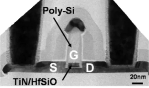
The next step in scaling SOI technologies is the use of Fully Depleted architecture to improve electrical behavior with reduced short channel effects. It allows extremely low voltage operations especially for mobile applications. In this paper, tested devices are FDSOI nMOS transistors with body contacts. This technology is developed at CEA/LETI-Minatec and is optimized for the 20 nm node [23]. The SOI active layer is 8-nm thick and the gate length varies from 10 m down to 30 nm. The BOX thickness is different from the one of the PDSOI technology studied in the previous section. A cross section of the transistor is represented in Fig. 6, where the gate stack made of a high-k dielectric layer topped by a metal-gate is presented. In such extremely thin SOI devices, radiation-induced charge trapping in both the front-gate oxide and in field oxides is a lower concern than the one related to trapping in the Buried Oxide (BOX) [14], [24]. In such transistors, the TID response is mainly governed by the radiation-induced holes trapped in the BOX, combined with electrostatic coupling effect inherent to FDSOI devices [25].
Oxide-trapped charge in the BOX can efficiently modify the potential in the whole silicon layer, inducing a shift of electrical characteristics. This mainly leads to an increased OFF-current and power consumption. It may also lock the transistor in the ON-case for a sufficiently high voltage shift is sufficiently high. Interface trap formation may also occur in addition to oxide-trapped charge buildup. Contrary to bulk and PDSOI devices, interface trap buildup occurring at the silicon-BOX interface can affect the transistor response due to electrostatic coupling effects. This may degrade the subthreshold slope and the drive current of static I–V characteristics, thus reducing
Fig. 7. Drain current vs gate voltage characteristics of planar FDSOI transistor with nm at several TID: before irradiation (black squares), 1 MGy (green triangles) and 3 MGy (red circles).
Fig. 8. Evolution of OFF-current (in log scale) vs TID for planar FDSOI tran-sistors with two different gate lengths: 40 nm (black squares) and 5 m (red circles). Irradiations are performed using a 10 keV X-ray laboratory source (small symbols) and using irradiations performed at Brigitte reactor located at SCK-CEN (large symbols at 0.5 MGy).
dynamic performances of integrated circuits. These mecha-nisms are depicted in Fig. 7 where static I–V measurements are presented at several total dose steps up to 3 MGy.
Transistor is grounded from pre-rad (black squares) up to 1 MGy (green triangles) to simulate an electronic component vol-untary left in a standby mode. From 1 MGy up to 3 MGy (red circles), the transistor is then turned on to account for normal operating conditions.
Fig. 7 highlights the previously explained behavior, with a voltage shift of electrical characteristics in addition to a signif-icant degradation of the subthreshold slope with TID. It is worth noting that this transistor remains functional after 3 MGy, without any particular hardening effort. This is very promising even if electrical performances appear degraded. Fig. 8 sum-marizes the evolution with TID for transistors with two different gate lengths: nm (black squares) and
m (red circles).
Even grounded, the transistor with the aggressive design nm exhibits a 2 orders of magnitudes increase of -current at 1 MGy during 10 keV X-ray irradiation. This is high enough to increase power consumption but it should be manageable for designers to maintain the Integrated
Fig. 9. Evolution of ON-current vs TID for planar FDSOI transistors with nm (black squares) and m (red circles). Irradiations are performed using a 10 keV X-ray laboratory source (small symbols) and using irradiations performed at Brigitte reactor located at SCK-CEN (large symbols at 0.5 MGy).
Circuit (IC) functional. After switching on the transistor, current increases by one additional order of magnitude at 3 MGy. This transistor, which is close to the nominal design for this technology, shows large variations in -current. It is sensitive to TID but this may be mitigated using hardening techniques, such as changing the geometry of the transistor. Only relaxing the transistor’s gate length leads to a much more limited impact on the current. As already stated in [14], radiation-induced hole trapped charge distributions are mainly governed by the electric field shape which stands in oxides. In that case, this leads to “pockets” of high trapped charge densi-ties mainly located at body-source and/or body-drain junctions as a function of the bias configuration during irradiation. For a short gate length, these pockets of high trapped charge densities into the BOX are long enough to start from the body-drain junction and to reach the body-source junction. A significant trapped charge density is trapped under the entire length of the transistor’s body modifying more efficiently the electrostatic potential through the entire thickness of the silicon layer due to coupling effects. By contrast, Relaxing the gate length thus leads to separate such pockets of high trapped charge densities less impacting the device response. Consequently, the transistor designed with a long gate length shows an shift which stays within the same decade up to 1 MGy; this is a satisfying result for a non-hardened technology.
However, both transistor designs exhibit large -current variations (see Fig. 9), with 60% decrease at 3 MGy. In such conditions, large margins are needed since transistors cur-rents govern the IC function to ensure safe operations.
Figs. 8 and 9 also exhibit results of -irradiations performed up to 500 kGy at Brigitte nuclear reactor facility located at SCK-CEN. In that case, devices are not biased during irradi-ation. Contrary to tests done using the X-ray laboratory source, devices are irradiated at a dose rate of 1.5 kGy/h in “real” op-erating conditions, combining -ray irradiation and tempera-ture stress at about 50 . Electrical characteristics are mea-sured several days after the end of irradiation. Both the - and -current measurements are consistent with 10 keV X-rays irradiation results. The limited difference can be explained by
Fig. 10. Schematic description of SOI FinFET/nanowire architecture and transversal TEM cross section [30].
several factors including charge yields related to 10 keV X-ray and irradiations [27]–[29], difference of temperature during irradiations and delays between irradiation and measurements. However, these preliminary results show similar trends, X-rays giving results close to those obtained under -ray irradiation even if measurements were not gathered in ideal conditions, de-vice qualification being not the topic of this paper.
Additional features of the presented curves, such as their shape, could be discussed. However, we choose to include data obtained on another technology (e.g., FinFETs, see Section III-D.) in MGy environment instead of detailing each curve shape related to physical mechanisms which is not the main topic of this paper.
D. SOI FinFET/Nanowire Technology
As presented in Section II-B, FinFET technology becomes more than a promising candidate for future commercial tech-nologies [15]. This architecture features multiple-gates to get an enhanced control of the electrostatic potential over the active sil-icon layer. Transistors now look like silsil-icon fingers surrounded by the gate stack made of a high-k dielectric and a metal-gate. The schematic configuration of SOI FinFET architecture (here with an -shaped gate) is displayed in Fig. 10, along with a transversal cross section [30].
Some studies have already shown that FinFET architecture may be intrinsically hardened to TID up to the 10 kGy (Mrad) level using appropriate geometry. Indeed, [16], [17] have demonstrated the fin width dependence of the TID response of multiple-gate FETs up to the 10 kGy range [16], [17], [31], [32]. Such devices should withstand high amount of TID even under normal operating conditions (biased). This is displayed in Fig. 11 where electrical characteristics obtained on a single-fin narrow SOI FinFET with a relaxed gate length m are given both before irradiation and after 3 MGy.
The SOI FinFET with long gate length exhibits an excellent TID tolerance. Neither the ON-current nor the OFF-current are significantly modified by radiation-induced oxide trap and in-terface trap charges. The strong potential control provided by the multiple-gates over the active silicon layer mainly reduces these effects. Similar results are obtained on the same devices grounded during irradiation.
Apparently, the subthreshold slope of FinFET devices slightly increases; this effect remains limited with regard to the number of silicon-oxide interfaces intrinsic to multiple-gate architectures. Obviously, such devices should be considered for
Fig. 11. Drain current vs gate voltage characteristics of a narrow SOI FinFET transistor with m before irradiation (black squares) and after 3 MGy (red circles). Device is drain-biased during irradiation.
Fig. 12. characteristics of bulk silicon, PDSOI, FDSOI and SOI FinFET technologies. Results are displayed as a function of TID for various geometries.
high TID environments when commercially accessible. Exper-iments are also performed on a FinFET with an aggressive gate length nm up to 500 kGy showing an equivalent promising TID tolerance. This means that the silicon finger width is the key parameter to ensure a good immunity to TID.
By contrast, wider SOI FinFETs do not exhibit this intrinsic TID tolerance. As expected, their behaviors under ionizing radi-ation look almost like the ones exhibited by planar FDSOI tran-sistors, with significant electrical characteristics modifications. Narrower the silicon fin, higher the TID tolerance.
IV. DISCUSSION
Fig. 12 summarizes the characteristics as a func-tion of TID of all devices tested in this paper: bulk silicon, PDSOI, FDSOI and SOI FinFET technologies. This figure-of-merit highlights the ability of one technology to withstand TID up to several MGy. The high-TID sensitivity of 0.18 m bulk devices (green) strongly depends on their design. Only edgeless transistors with enclosed layout geometry can withstand high irradiation level. The apparent reduction would probably be reduced using a much more scaled bulk technology with a thinner gate oxide. 0.13 m PDSOI devices with body contacts exhibit a high level of TID hardening.
Only the leakage current increases due to the triggering of the parasitic back transistor. The drive current is insen-sitive to TID and increases only when devices are biased during irradiation. When devices are grounded during irradia-tion, neither the current nor the current are modified. Few efforts are needed to harden such devices to MGy doses. Only the parasitic back transistor has to be mitigated to improve the radiation tolerance of this technology.
Among other advanced technologies, SOI FinFET seems to meet the requirements needed for safe operation in MGy environments. In the results presented here, -currents of FinFETs are strongly lower than FDSOI ones because only single-fin devices are tested. No significant shifts are obtained on SOI FinFETs results (red), not only for the ON-current but also for the OFF-current. variations are within the measurement uncertainty (see Fig. 11, ), varia-tions on this parameter should not be taken into account. This intrinsic immunity to TID of SOI FinFETs has to be checked on bulk FinFETs presented in [15]. Indeed, the first study on similar multiple-gate bulk transistors has concluded to an opposite behavior [33]: wide bulk FinFETs show a promising TID tolerance when optimized narrow bulk FinFETs exhibit a higher TID sensitivity. Actually, number of STI/active silicon interfaces occur in such narrow bulk transistors with multiple fins, even processed with multiple gates. Their TID response will then be mainly governed by the radiation-induced charge trapping in STIs which may trigger a strong Radiation-Induced Narrow Channel Effect as already observed in [6], [34] on planar bulk transistors.
On the other hand, planar FDSOI exhibits a promising be-havior to operate in harsh environment with appropriate device architecture, despite modifications of their electrical character-istics with TID.
Fig. 12 presents trends on the high TID response of elemen-tary devices fabricated in several technologies since it is the main issue discussed in this paper. However, one has to take in mind that these technologies strongly differ by their tech-nology node, substrate type (bulk or SOI), architecture (planar or FinFET) and distributions of high TID responses will be obtained for each technology if a great number of devices would have been tested. These distributions would appear in Fig. 12 as clouds of points around the ones depicted in Fig. 12 for each tested device without changing the overall trend. So, this would give an image of the variability intrinsic to each fabrication process and its related ionizing radiation response.
V. CONCLUSION
This paper investigates the vulnerability of commercial bulk and PDSOI technologies along with state-of-the-art advanced FDSOI and SOI FinFET under MGy dose environment which may be encountered in future nuclear power plants or deep space missions. They are studied using dedicated experiments on n-channel Metal-Oxide Semiconductor Field Effect Tran-sistors (MOSFETs) to draw first trends on their behavior under high TID. Bulk and PDSOI technologies present low TID sensitivity using the appropriate device design but without any hardening of field oxides or doping engineering. As already observed in the literature at lower TID (about 10 kGy i.e.,
1 Mrad) FDSOI devices show large modifications of their electrical characteristics, mainly due to radiation-induced hole trapping in the buried oxide. This is an issue for circuit power consumption but the most critical one is the strong reduction of ON-current at high TID whatever the geometry. By contrast, similar experiments performed on narrow SOI FinFETs demonstrate their intrinsic tolerance to MGy doses without particular hardening effort. Neither the ON-current nor the OFF-current are significantly modified after 3 MGy (300 Mrad), meaning that circuit functionality should be safely ensured as well as a low power consumption compatible with stand alone operations.
REFERENCES
[1] IAEA-TECDOC-118, Assessment and Management of Ageing of
Major Nuclear Power Plant Components Important to Safety: In Containment Instrumentation and Control Cables, 2000.
[2] NF M64-001, Procedure de qualification des matériels électriques
in-stallés dans l’enceinte de confinement des réacteurs à eau sous pres-sion et soumis aux conditions accidentelles, 1991.
[3] D. Fleetwood, “How to protect nuclear reactor electronics,” IEEE
Spectrum Tech Talk, 2011.
[4] A. H. Johnston, “Space radiation effects and reliability considerations for micro- and optoelectronic devices,” IEEE Trans. Device Mater.
Re-liab., vol. 10, no. 4, p. 449, 2010.
[5] R. Lacoe, “Designing radiation hardened CMOS microelectronic com-ponents at commercial foundries: Space and terrestrial environments and device and circuit techniques to mitigate radiation effects,” in Proc.
IEEE Int. Integr. Reliab. Workshop Final Rep., 2005, p. 143.
[6] F. Faccio and G. Cervelli, “Radiation-induced edge effects in deep sub-micron CMOS transistors,” IEEE Trans. Nucl. Sci., vol. 52, no. 6, p. 2413, Dec. 2005.
[7] EPR Safety, Security and Environmental Report, “Fundamental Safety Overview, volume 2: Design and Safety” Sub-Chapter C7, “Qualifica-tion of Electrical and Mechanical Equipment for Accident Condi“Qualifica-tions”. [8] [Online]. Available:
http://www.asn.fr/index.php/S-informer/Ac- tualites/2012/Rapport-del-ASN-sur-les-evaluations-complemen-taires-de-surete-ECS
[9] J. Verbeeck, M. Van Uffelen, M. Steyaert, and P. Leroux, “Conceptual design of a MGy tolerant integrated signal conditioning circuit in 130 nm and 700 nm CMOS,” in Proc. Topical Workshop Electron. Particle
Physics, 2011, pp. 1–8.
[10] J. L. Leray, “Activation energies of oxide charge recovery in SOS or SOI structures after an ionizing pulse,” IEEE Trans. Nucl. Sci., vol. 32, no. 6, pp. 3921–3928, Dec. 1985.
[11] J. L. Leray, E. Dupont-Nivet, J. F. Pere, O. Musseau, P. Lalande, and A. Umbert, “Limiting factors for SOI VLSI high-level hardness: Modeling and improving,” in Proc. SOS/SOI Technol. Conf., 1989, pp. 114–115.
[12] J. L. Leray, E. Dupont-Nivet, J. F. Pere, Y. M. Coïc, M. Raffaelli, A. J. Auberton-Hervé, M. Bruel, B. Giffard, and J. Margail, “CMOS/SOI hardening at 100 ,” IEEE Trans. Nucl. Sci., vol. 37, no. 6, pp. 2013–2019, 1990.
[13] P. Gouker, J. Burns, P. Wyatt, K. Warner, E. Austin, and R. Mi-lanowski, “Substrate removal and BOX thinning effects on total dose response of FDSOI NMOSFET,” IEEE Trans. Nucl. Sci., vol. 50, no. 6, pp. 1776–1783, Dec. 2003.
[14] J. R. Schwank, V. Ferlet-Cavrois, M. R. Shaneyfelt, P. Paillet, and P. E. Dodd, “Radiation effects in SOI technologies,” IEEE Trans. Nucl.
Sci., vol. 50, no. 3, pp. 522–538, Jun. 2003.
[15] [Online]. Available: http://www.intel.com/content/www/us/en/sil-icon-innovations/intel-22nm-technology.html
[16] M. Gaillardin, P. Paillet, V. Ferlet-Cavrois, S. Cristoloveanu, O. Faynot, and C. Jahan, “High tolerance to total ionizing dose of -shaped gate field-effect transistors,” Appl. Phys. Lett, vol. 88, p. 223511, 2006.
[17] M. Gaillardin, P. Paillet, V. Ferlet-Cavrois, O. Faynot, C. Jahan, and S. Cristoloveanu, “Total ionizing dose effects on triple-gate FETs,” IEEE
Trans. Nucl. Sci., vol. 53, no. 6, p. 3158, Dec. 2006.
[18] N. Rezzak, M. L. Alles, R. D. Schrimpf, S. Kalemeris, L. W. Massen-gill, J. Sochacki, and H. J. Barnaby, “The sensitivity of radiationin-duced leakeage to STI topology and sidewall doping,” Microelectron.
Reliab., vol. 51, pp. 889–894, 2011.
[19] M. R. Shaneyfelt, P. E. Dodd, B. L. Draper, and R. S. Flores, “Chal-lenges in hardening technologies using shallow trench isolation,” IEEE
Trans. Nucl. Sci., vol. 45, no. 6, pp. 2584–2592, Dec. 1998.
[20] V. Ferlet-Cavrois, T. Colladant, P. Paillet, J. L. Leray, O. Musseau, J. R. Schwank, M. R. Shaneyfelt, J. L. Pelloie, and J. du Port de Pontcharra, “Worst-case bias during total dose irradiation of SOI transistors,” IEEE
Trans. Nucl. Sci., vol. 47, no. 6, pp. 2183–2188, Dec. 2000.
[21] M. Rezzak, E. X. Zhang, M. L. Alles, R. D. Schrimpf, and R. D. Hughes, “Total-Ionizing-Dose radiation response of partially-depleted SOI devices,” in Proc. IEEE SOI Conf., 2010, pp. 1–2.
[22] P. E. Dodd, M. R. Shaneyfelt, J. R. Schwank, and J. A. Felix, “Current and future challenges in radiation effects on CMOS electronics,” IEEE
Trans. Nucl. Sci., vol. 57, no. 4, pp. 1747–1763, Aug. 2010.
[23] C. Fenouillet-Beranger, P. Perreau, S. Denorme, L. Tosti, F. An-drieu, O. Weber, S. Barnola, C. Arvet, Y. Campidelli, S. Haendler, R. Beneyton, C. Perrot, C. de Buttet, P. Gros, L. Pharn-Nguyen, F. Leverd, P. Gouraud, F. Abbate, F. Baron, A. Torres, C. Laviron, L. Pinzelli, J. Vetier, C. Borowiak, A. Margain, D. Delprat, F. Boedt, K. Bourdelle, B.-Y. Nguyen, O. Faynot, and T. Skotnicki, “Impact of a 10-nm UltraThin BOX (UTBOX) and Ground Plane on FDSOI Devices for 32 nm and below,” in Proc. ESSDERC, 2009.
[24] P. Paillet, M. Gaillardin, V. Ferlet-Cavrois, A. Torres, O. Faynot, C. Jahan, L. Tosti, and S. Cristoloveanu, “Total ionizing dose effects on deca-nanometer fully depleted SOI devices,” IEEE Trans. Nucl. Sci., vol. 52, no. 6, p. 2345, Dec. 2005.
[25] H. K. Lim and J. G. Fossum, “Threshold voltage of thin film Silicon-on-Insulator (SOI) MOSFET’s,” IEEE Trans. Electron Dev., vol. ED-30, no. 10, p. 1244, Oct. 1983.
[26] L. Brunet, X. Garros, M. Cassé, O. Weber, F. Andrieu, C. Fe-nouillet-Béranger, P. Perreau, F. Martin, M. Charbonnier, D. Lafond, C. Gaumer, S. Lhostis, V. Vidal, L. Brévard, L. Tosti, S. Denorme, S. Barnola, J. F. Damlencourt, V. Loup, G. Reimbold, F. Boulanger, O. Faynot, and A. Bravaix, “New insights on Vt stability of HK/MG stacks with scaling in 30 nm FDSOI technology,” in Proc. Symp. VLSI
Technol. Dig. Tech. Papers, 2010, p. 29.
[27] C. M. Dozier, D. M. Fleetwood, D. B. Brown, and P. S. Winokur, “An evaluation of low energy X-ray and cobalt-60 irradiation of MOS tran-sistors,” IEEE Trans. Nucl. Sci., vol. NS-34, no. 6, pp. 1535–1539, Dec. 1987.
[28] M. R. Shaneyfelt, D. M. Fleetwodd, J. R. Schwank, and K. L. Hughes, “Charge yield for Cobalt-60 and 10-keV X-ray irradiations of MOS devices,” IEEE Trans. Nucl. Sci., vol. 38, no. 6, pp. 1187–1194, Dec. 1991.
[29] P. Paillet, J. R. Schwank, M. R. Shaneyfelt, V. Ferlet-Cavrois, R. L. Jones, O. Flament, and E. Blackmore, “Comparison of charge yield in MOS devices for different radiation sources,” IEEE Trans. Nucl. Sci., vol. 49, no. 6, pp. 2656–2661, Dec. 2002.
[30] C. Jahan, O. Faynot, M. Casse, R. Ritzenthaler, L. Brevard, L. Tosti, X. Garros, C. Vizioz, F. Allain, A.-M. Papon, H. Dansas, F. Martin, M. Vinet, B. Guillaumot, A. Toffoli, B. Giffard, and S. Deleonibus, “OmegaFETs transistors with TiN metal gate and HfO2 down to 10 nm,” in Proc. Symp. VLSI Technol. Dig. Tech. Papers, 2005, pp. 112–113.
[31] J. P. Colinge, A. Orozco, J. Rudee, W. Xiong, C. Rinn Cleavelin, T. Schulz, K. Schrufer, G. Knoblinger, and P. Patruno, “Radiation dose effects in trigate SOI MOS transistors,” IEEE Trans. Nucl. Sci., vol. 53, no. 6, pp. 3237–3241, Dec. 2006.
[32] F. ElMamouni, E. X. Zhang, R. D. Schrimpf, D. M. Fleetwood, R. A. Reed, S. Cristoloveanu, and W. Xiong, “Fin-width dependence of ionizing radiation-induced subthreshold swing degradation in 100-nm gate-length FinFETs,” IEEE Trans. Nucl. Sci., vol. 56, no. 6, pp. 3250–3255, Dec. 2009.
[33] S. Put, E. Simoen, M. Jurczak, M. Van Uffelen, P. Leroux, and C. Claeys, “Influence of fin width on the total dose behavior of p-channel bulk MugFETs,” IEEE Electron Dev. Lett., vol. 31, no. 3, pp. 243–245, 2010.
[34] M. Gaillardin, V. Goiffon, S. Girard, M. Martinez, P. Magnan, and P. Paillet, “Enhanced radiation induced narrow channel effects in a com-mercial 0.18 m bulk technology,” IEEE Trans. Nucl. Sci, vol. 58, no. 6, p. 2807, Dec. 2011.
![Fig. 10. Schematic description of SOI FinFET/nanowire architecture and transversal TEM cross section [30].](https://thumb-eu.123doks.com/thumbv2/123doknet/3562274.104354/7.888.86.403.95.325/schematic-description-finfet-nanowire-architecture-transversal-cross-section.webp)
