Competition between deep impurity and dopant behavior
of Mg in GaN Schottky diodes
M. Schmeits,a)N. D. Nguyen, and M. Germain
Institute of Physics, University of Lie`ge, B4000 Sart-Tilman/Lie`ge, Belgium 共Received 18 July 2000; accepted for publication 13 November 2000兲
The effect of the deep acceptor Mg on the electrical characteristics of p-doped GaN Schottky diodes is analyzed. The theoretical study is based on the numerical resolution of the basic semiconductor equations, including the continuity equation for the Mg-related acceptor level. It gives the steady-state and small-signal analysis of p-doped GaN:Mg Schottky diodes, yielding as final result the frequency dependent capacitance and conductance of the structure. It is shown that the low-frequency characteristics are determined by the carrier exchange between the Mg related impurity level and the valence band, whereas above the impurity transition frequency, the hole modulation of the depletion layer edge governs the electrical response. Detailed results are shown on the effect of temperature, applied steady-state voltage and series resistance. The study of two back-to-back connected GaN Schottky diodes reveals the appearance of typical features in the electrical characteristics, depending on the respective Schottky barrier height of the two junctions. © 2001 American Institute of Physics. 关DOI: 10.1063/1.1339208兴
I. INTRODUCTION
The wide-gap semiconductor gallium nitride has re-ceived much attention during the past decade. It is consid-ered as a basic material for visible and UV light emitters and UV visible blind detectors.1–4 GaN-based bipolar junction transistors and heterojunction field effect transistors are an-other potential application field.5,6
The need for both n-type and p-type dopants for the realization of practical structures has led to active research to find the most efficient atomic impurities. For wide-gap semi-conductors like SiC and GaN, Si is used as shallow n dopant. However, shallow p dopants do not exist. Rapid progress was obtained when p-type conduction by Mg doping with appropriate posttreatment was achieved. Magnesium is con-sidered as a deep dopant with activation energies given in the literature in the range of 120–250 meV, the most frequently cited values being around 150–170 meV.7–9 We label the total Mg concentration Nt and nt is the concentration of oc-cupied Mg levels.
With these values of the acceptor ionization energy, Mg acts simultaneously as a dopant and as a deep impurity. Shal-low dopants are considered as fully ionized, at least for all temperatures of practical interest. The Mg acceptor level is only partially ionized for these temperature ranges. At ther-mal equilibrium, its occupation is fixed by the relative posi-tion of the defect level with respect to the Fermi energy. This in turn results from the charge neutrality condition, which contains the ionized acceptor charge qntas one of its terms. Mg acts as dopant, providing free holes for the valence band, but less than the total Mg concentration. In a junction, at the depletion layer edge, the hole concentration varies from zero to a maximum value, which is the total acceptor concentra-tion in the case of shallow dopants but which is less in the
case of Mg doping. This influences the contribution of the modulation of the depletion layer edge to the total junction capacitance.
When used in a p–n junction or in a metal/GaN-p Schottky diode, the Mg-related acceptor level may cross the hole quasi-Fermi level. The modulation of the applied volt-age modifies the occupation of the Mg-related energy level and gives rise to typical features in the electrical character-istics. This behavior is similar to that of deep impurities,10–12 but with the difference that the crossing point here separates regions where the concentration of the occupied levels is respectively Nt and nt, i.e., the impurity levels are totally ionized and partially ionized. In the classical deep impurity case, however, these concentrations are, respectively, Ntand zero.
As the value of nt is strongly temperature dependent, important effects in the study of electrical characteristics as a function of temperature can be expected. We will effectively show that this is the case and that moreover, in the resulting response to an applied voltage modulation, there is a compe-tition between the contribution of the modulated defect state population and the hole concentration at the depletion layer edge. For low frequencies, in the classical deep impurity context, both act simultaneously and independently. In the deep dopant case however we will show that, at low frequen-cies, the holes provided by the modulating source contribute mainly to the modulation of the occupation of the Mg-related energy level and only in a minor way to the modulation of the depletion layer edge. Above the defect transition fre-quency however, the hole response increases, remaining the only contribution to the junction capacitance.
Experimental studies of the electrical characteristics of Mg-doped GaN Schottky diodes have been reported in Refs. a兲Electronic mail: m.schmeits@ulg.ac.be
1890
13 and 14. Depletion region effects in GaN p–n junctions have been discussed by Kozodoy et al.15
The aim of this article is to present a theoretical study of the role of Mg in the electrical characteristics of GaN Schottky diodes, performing the detailed steady-state and small-signal analysis of a Schottky diode containing Mg-related deep acceptor levels. It starts from the numerical resolution of the basic coupled semiconductor equations, i.e., Poisson’s equation and the continuity equations for elec-trons, holes and occupied impurity levels. This yields position-dependent values of the electrical potential, the en-ergy band diagrams, the carrier concentrations, the current densities and the carrier recombination rates. As a final re-sult, one obtains the electrical admittance Y, whose real part is the conductance G, and the imaginary part yields the total junction capacitance. This allows us to study in detail the influence of each microscopic parameter corresponding ei-ther to the material, the impurity, the junction, or the experi-mental conditions on the resulting macroscopic electrical quantities.
In the applications, we will determine the effect of the temperature T, the applied steady-state voltage and the series resistance. Finally, systems consisting of a double Schottky diode, i.e., two Schottky diodes connected back to back will be considered.
II. BASIC EQUATIONS AND NUMERICAL PROCEDURE
GaN is classified as a wide-gap semiconductor, with a room-temperature gap of 3.4 eV. Mg is giving rise to several impurity states with energies inside the gap. There is com-mon agreement that there is one acceptor state whose energy position Et is at 150–170 meV above the valence band edge.7–9 In the numerical applications, we will take Et ⫽160 meV for the activation energy. The total Mg concen-tration will be labeled Nt, with notations similar to those used for deep impurities.16 Other eventually present shallow donor or acceptor concentrations are labeled ND and NA, respectively. The concentration of occupied defect levels for thermal equilibrium at temperature T is given by17
nt⫽
Nt
1⫹g exp关共Et⫺EF兲/kT兴
, 共1兲
where g is the degeneracy factor, k the Boltzmann constant, and EFis the Fermi energy; g is assumed to equal 4, a value characteristic of acceptor levels.17 The hole concentration p is given by
p⫽Nvexp关共Ev⫺EF兲/kT兴, 共2兲
where Nv is the effective valence band density of states. The electron concentration n can be expressed similarly. The equilibrium Fermi energy EFis obtained by solving numeri-cally the charge neutrality condition which writes for accep-tor levels
p⫺n⫹ND⫺NA⫺nt⫽0. 共3兲
The shallow dopants are supposed completely ionized. With a hole effective mass mh⫽0.8 m0
7
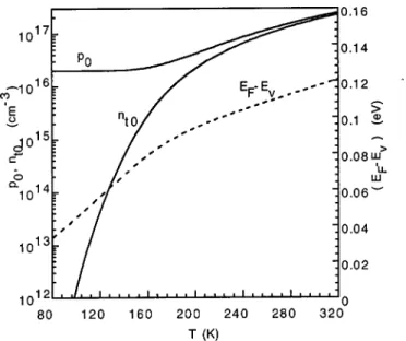
, Nt⫽4⫻1018 cm⫺3, ND ⫽0, and NA⫽2⫻1016cm⫺3, the thermal equilibrium values
as function of temperature T of (EF– Ev), nt, and p are given in Fig. 1. In this temperature range, the Fermi level is pinned at a value between the valence band edge Ev and the defect energy Et. The equilibrium hole concentration is at least equal to NA, increasing with temperature in a similar way to nt. At room temperature共RT, T⫽293 K兲, nt reaches a value of 1.6⫻1017cm⫺3, which corresponds to about 4% of ionized acceptors.
The transition rates for electrons between the level Et and the valence band are given according to the Shockley–Read–Hall16scheme by
rpt共Et兲⫽cppnt⫺ep共Nt⫺nt兲, 共4兲
where cp is the capture rate for holes, expressed in terms of the hole thermal velocity vth
p and the hole thermal capture cross section p by
cp⫽vth
p
p. 共5兲
The thermal emission rate ep is given by ep⫽cp
g Nvexp关共Ev⫺Et兲/kT兴. 共6兲
Similar expressions hold for the electron to conduction band transition rates rnt. Carrier exchanges with the conduc-tion band in this case plays only a minor role, as the defect energy position is close to the valence band edge. The elec-trical potential⌿ and the carrier concentrations n, p and nt have to satisfy the basic semiconductor equations, namely Poisson’s equation and the continuity equations for elec-trons, holes, and occupied defect levels.18,19
“共“兲⫽⫺q共p⫺n⫹ND⫺NA⫺nt兲, 共7a兲
n t ⫽
1
q “•Jn⫺rnt, 共7b兲
FIG. 1. GaN bulk Fermi level position in thermal equilibrium relative to the valence band edge, for Et– Ev⫽0.16 eV, Nt⫽4⫻10
18cm⫺3, and N A⫽2
⫻1016 cm⫺3. Steady-state bulk hole concentration p0 and occupied
p t ⫽ ⫺ 1 q “•Jp⫺rpt, 共7c兲 nt t ⫽rnt⫺rpt, 共7d兲
where Jn and Jp are, respectively, the electron and hole cur-rent densities
Jn⫽nn“ Ec⫹nkT“ n, 共8a兲
Jp⫽pp“ Ev⫺pkT“ p, 共8b兲
where n and p are the electron and hole mobilities, q is the electronic charge.
For the steady-state equations for a given value of tem-perature T and applied voltage V0, the left-hand side of
re-lations 共7兲 is equal to zero. In the small signal analysis, the applied voltage contains in addition to the steady-state value V0, a sinusoidally modulated term of frequency f⫽/2
and of amplitude V˜ , small with respect to kT/q
V⫽V0⫹V˜ eit. 共9兲
In the small-signal analysis, all quantities will have a dc component which will be given with an index ‘‘ 0’’ and a harmonic component whose amplitude, labeled with a tilde, is complex in the general case. For example, the hole con-centration writes
p共x,t兲⫽p0共x兲⫹p˜共x兲 eit. 共10兲
Explicit expressions for the ac components are given in Ref. 20.
In the numerical study, the system is considered as one dimensional, with x giving the position. The position of the left boundary and right boundary of the region occupied by the semiconducting material are, respectively, xL and xR.
We place the Schottky contact at x⫽xL. In the boundary conditions, the Schottky barrier height qb is fixed. In ther-mal equilibrium it is related to the built-in potential Vbi and the bulk separation between the Fermi energy EF and the depletion layer edge Ev by17
qb⫽qVbi⫹共EF⫺Ev兲. 共11兲
In addition, a finite surface recombination velocity has to be given to fully characterize the metal–semiconductor contact.18 At x⫽xR, ohmic contact conditions are imposed when a single junction is considered. Some results will be given for back-to-back Schottky contacts, and in that case similar boundary conditions are imposed for both contacts.
Instead of using the variables⌿, n, p, and nt, the Eqs. 共7a兲–共7d兲 are expressed in terms of and the quasi-Fermi energies Fn, Fp, and Ft, as these are more appropriate, giving variations of the same order of magnitude for the four unknowns. The set of Eqs.共7a兲–共7d兲 is then solved numeri-cally, after scaling and discretization according to a variable size mesh. As results one obtains the steady-state and small signal values of the electrical potential⌿, the concentrations n, p, nt, the recombination rates rnt and rpt, the current densities Jn and Jp and the displacement current JD, in the ac case. The total ac current density J˜ is constant with
re-spect to x. From its value, one obtains the admittance Y ⫽J˜/V˜, from which the total capacitance C and conductance G can be obtained
Y⫽G⫹iC. 共12兲
Both G and C depend on the frequency f, the steady-state voltage V0, and the temperature T.
III. NUMERICAL RESULTS
A. Schottky GaN:Mg junction under room temperature, zero-bias conditions
We start by the study of a rectifying metal/GaN:Mg junction for which the chosen set of parameters corresponds to typical values resulting from experimental analysis.7–9,21–24 The activation energy of the Mg acceptor level is taken at 共 Et– Ev)⫽0.16 eV. The Schottky barrier
height qb is taken 0.70 eV.21–23The hole surface recombi-nation velocity is taken 109 cm/s. The deep and shallow dop-ant concentrations are, respectively, Nt⫽4⫻1018cm⫺3, NA ⫽2⫻1016 cm⫺3. The total length of the device is chosen as
20 m, such that series resistance effects are of moderate importance. The hole thermal cross section is p⫽2 ⫻10⫺20 cm2;24
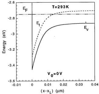
and the hole mobility is p⫽10 cm2/V s8. The resulting energy band diagram for T⫽293 K and zero bias is given in Fig. 2. The bulk hole concentration is p0 ⫽1.8⫻1017cm⫺3and represents a relatively strong effective
doping, producing a depletion layer edge at 0.020 m, this edge being not totally abrupt. The defect state crosses the equilibrium Fermi level at a distance of 0.014m from the left metal/semiconductor interface.
In Fig. 3, we represent for the same conditions, the steady-state concentrations nt0(x) and p0(x) as function of position x, together with the absolute values of the small-signal amplitudes n˜t(x) and p˜ (x). The latter have been cal-culated for three different frequencies 关low 共LF兲, medium
FIG. 2. Metal/GaN-p Schottky contact energy diagram for RT and zero-bias conditions. Mg acceptor level is at 0.16 eV above the valence band edge. Schottky barrier height is 0.7 eV. Left limit of semiconducting region is at xL⫽⫺10m.
共MF兲, and high共HF兲兴, f ⫽102 Hz共LF兲, 3⫻103 Hz共MF兲, and
105 Hz 共HF兲, the notations used becoming clear in the fol-lowing. At low frequency, this absolute value is practically equal to the real part n˜t
R
, changed by sign. Having chosen the voltage amplitude V˜ real, n˜tR is negative. At low fre-quency, n˜t(x) presents a peak at a distance of 0.01m from the junction, a position where nt0(x) is at about 50% of its maximum value; p˜ (x) presents its maximum value at 0.017 m from the left boundary. These responses remain approxi-mately constant up to 5⫻102Hz, i.e., as long as the impurity states are able to completely follow the variations of the applied voltage. With increasing modulation frequency, the amplitude n˜t(x) decreases as expected, reaching at the HF frequency a value reduced by about a factor 102with respect to the low frequency value. The variation of p˜ (x) with fre-quency is however different. It does not simply remain
con-stant above the impurity transition frequency, but increases above the MF frequency, reaching in the HF regime a value which is by a factor of 10 larger than the LF value.
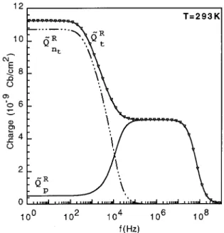
The same behavior is illustrated in Fig. 4, where one shows, as function of frequency, the real part of the charges related to the amplitude of the impurity level concentration, hole concentration, and charge density. These are defined as
Q˜n t R⫽q
冕
xL 0 兩n˜t R兩 dx, 共13a兲 Q˜pR⫽q冕
xL 0 p ˜R共x兲 dx, 共13b兲 Q˜t R⫽q冕
xL 0 共p˜R⫺n˜ t R兲 dx. 共13c兲The upper limit of the integration given here is largely above the x values where the integrands are of negligible value; x⫽0 represents here (XR– XL)/2.
These curves show that the modulated space charge con-tribution due to the exchange of carriers between the Mg-related impurity level and the valence band goes to zero at a transition frequency of 4⫻103 Hz. At the same time, as the impurity response decreases, the response of the holes at the depletion layer edge increases, keeping a constant value up to 107 Hz. Above this value, the hole response goes to zero with a cutoff frequency corresponding, in electrical terms, to the RC cutoff frequency of a RC series circuit, where C is the depletion-layer capacitance and R the series resistance. The modulation of the total charge Q˜tR is the resulting sum of both contributions, where the LF contribution is due essen-tially to the response of the impurity level and the HF con-tribution is due essentially to the holes modulating the deple-tion layer edge. The LF contribudeple-tion of the holes exists in this case, because a nonzero value of the shallow acceptor concentration NA has been assumed. Without this term, Q˜p R
FIG. 3. Steady-state impurity concentration nt0and hole concentration p0, as function of position x, for RT and zero-bias conditions. Absolute value of small-signal ac amplitude for three frequencies of the applied ac voltage f
⫽102Hz共LF兲, f ⫽5⫻103Hz共MF兲, f ⫽105Hz共HF兲.
FIG. 4. Integrated absolute value of the real part amplitude of the ac re-sponse of q n˜t, q p˜ , q(n˜t⫺p˜).
would have been zero in the LF case. Dividing Q˜tR by the amplitude of the ac voltage yields V˜ yields nothing but the capacitance of the whole structure.
This behavior is obviously different from that of p–n junctions or Schottky diodes containing shallow, fully ion-ized dopants and deep impurities, with concentrations of the shallow dopants larger than those of the impurities.10–12Here the hole共or electron兲 response resulting from the modulation of the depletion layer edge remains constant over the entire frequency range, yielding a constant共called HF兲 capacitance term. The contribution of the impurity level exchanging car-riers with the valence 共or conduction兲 band gives an addi-tional contribution from zero frequency up to the transition frequency where the impurity levels no longer respond to the applied voltage. Here, the Mg level acts simultaneously as dopant and deep impurity. Depending on frequency, there is a competition between the two functions. In the LF range, the holes provided by the modulating voltage source essen-tially modify the charge on the impurity level. When these are no longer able to follow the applied voltage modulation, the holes contribute to the modulation of the depletion layer charge, but with a stronger amplitude than in the LF regime.
B. Effect of applied steady-state voltageV0
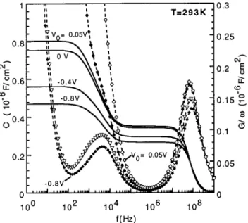
In Fig. 5, we show as a function of frequency and for different values of the steady-state voltage V0 the resulting
variations of the capacitance C and of G/. The curve of G/ presents a peak at the cutoff frequencies of the capacitance, or at least a shoulder when the conductance G is too large. As the reverse voltage increases, the capacitance decreases both in the LF and the HF regimes. The plot of the inverse square values of CLF and CHF as function of V0 yields,
within the particular values if the parameters we have used, a
straight line. However, care should be taken before directly applying textbook relations in order to determine dopant concentrations or built-in voltages.
C. Effect of series resistance
The series resistance in a structure depends on the dis-tance separating the ohmic contact from the depletion layer edge, in our case this is essentially (xL– xR). It also depends on the geometry of the structure, which in many cases has not a linear configuration. Gallium nitride is often grown on a sapphire substrate, on which it is impossible to realize con-tacts of either ohmic or Schottky type. The concon-tacts are therefore evaporated on top of the GaN layer.
We have considered different cases, simulating these ef-fects. In Fig. 6, curve 共A兲 corresponds to the previously treated case, with l⫽(xL– xR)⫽20m andp⫽10 cm2/V s. For curve 共B兲, the length is taken l⫽1000 m, all other parameters remaining constant. This causes a shift of the RC cutoff frequency by a factor 50, the rest of the C(f) curve is unmodified. For curve共C兲, the hole mobility of GaN outside the depletion region has been divided by a factor 200. In a one-dimensional analysis, cylindrical symmetry along the x axis is implicit. The reduction of the mobility would simulate a three-dimensional structure where the conduction channel has a cross section much smaller than the metallic contacts. This is, for example, the case in a planar structure where contacts of about 1 mm2section are realized on a GaN layer whose thickness is in the micrometer range. In this case, as seen on curve共C兲, the RC cutoff frequency has moved below the impurity transition frequency. The new cutoff frequency of 2⫻103 Hz corresponds to the RC cutoff frequency, where R is still the series resistance Rsand C is now the LF capaci-tance, due essentially to the response of the impurity level. The electrical character governs the response of the system, irrespective of the microscopic origin of the capacitance. It
FIG. 5. Capacitance per unit section C and conductance per unit section G over, as function of frequency f for RT conditions, for metal /GaN:Mg junction with applied steady-state voltages V0⫽⫹0.05, 0, ⫺0.4, and ⫺0.08 V. Length of the structure is (xR– xL)⫽20m. Hole mobility ish⫽10 cm2/V s.
FIG. 6. Capacitance per unit section C and conductance per unit section G over, of Schottky junction with parameters of Fig. 5,共curve A兲, length multiplied by factor 50共curve B兲, length multiplied by factor 50, and mo-bility divided by factor 200共curve C兲.
should be mentioned that the low frequency value of the capacitance remains unmodified by the change in series sistance, as this latter produces no modifications in the re-gion where the occupation of the impurity level changes.
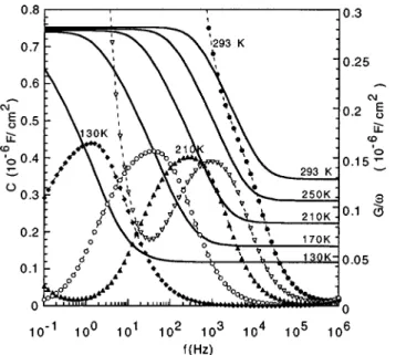
D. Effect of temperature
Modifying the temperature is expected to produce ef-fects at several levels. It modifies the position of the equilib-rium Fermi level EF relative to the valence band edge. The value of the energy gap and of the impurity activation energy are assumed to remain constant with T. Temperature also affects the occupation of the Mg level and the hole equilib-rium concentration in the valence band, as well as the ther-mal transition rates rpt. In Fig. 7, we show the C–f and G/ curves for temperatures T⫽293, 250, 210, 170, and 130 K. The low frequency capacitance remains nearly constant with temperature, whereas the HF capacitance decreases with T. This latter effect is clearly a consequence of the reduction of the hole concentration in the valence band. The transition frequency ft between the LF and the HF values decreases with temperature. Assuming this frequency equal to the ther-mal emission rate ep, divided by 2, would give a tempera-ture dependence of the type
ft⬀ T2exp共⫺⌬E*/kT兲, 共14兲
where ⌬E* should be in principle equal to (Et– Ev), the impurity ionization energy. A plot of the numerically ob-tained transition frequencies as function of 1/kT yields, in our particular case, a value of⌬E*⫽0.115 eV, which is less
than the used value of (Et– Ev)⫽0.160 eV. By writing ft ⫽ep/2, several terms are neglected already in the classical case.25In addition, the original relation has been established in a context which is not fully realized in the case treated here. It effectively assumes a concentration of fully ionized
shallow dopants, with a concentration larger than the deep impurity concentration and both entities being of a distinct nature.
IV. BACK-TO-BACK CONNECTED SCHOTTKY DIODES
In experimental situations, one may meet configurations where the electrical measurements are performed on samples with two identical contacts, which both are of Schottky type. In that case, it is necessary to describe both contacts as Schottky junctions. In the numerical treatment used here, this presents no major difficulty, as it needs only to set the ap-propriate boundary conditions on the second contact.
In the case of a symmetric double Schottky diode, with homogeneous doping and impurity concentrations and with the same value of the Schottky barrier height qb⫽0.70 eV at the left and right contact, the resulting amplitudes of the carrier concentrations are antisymmetric with respect to the center of the structure x⫽0. This is illustrated in Fig. 8 where we show the real part of n˜t, for x values close to both semiconductor/metal interfaces. The resulting capacitance– frequency curves for the V0⫽0 case have the same shape
than those shown in Fig. 3, except that all values are divided by a factor of about 2, as in that case the voltage is applied to a system which consists essentially of two identical diodes placed in series.
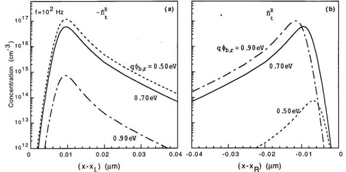
In order to study the effect of the asymmetry of the contacts, we have treated two other cases, where the Schottky barrier height has been kept equal to qb⫽0.70 eV at the left contact, but set equal to respectively 0.50 and 0.90 eV on the right contact. This leads to completely different ac-impurity occupation functions in the two sides of the structure. As shown in Fig. 8, the amplitude of n˜tR is stron-gest on the side where the Schottky barrier is larstron-gest. The weakest barrier seems to have a behavior similar to that of an ohmic contact. This feature is illustrated in Fig. 9, where we show for the case where qb⫽0.90 eV at the right contact, the values of the integrated real parts of the carrier ampli-tudes. The integrations are performed on x values close to the respective contacts. The resulting functions are drastically different from those shown in Fig. 4. The low frequency part of the modulated space charge has now two contributions, one from the right contact, below 104 Hz, and one from the left contact, centered at 5⫻102 Hz. The HF contribution of the holes is of equal importance on both sides of the struc-ture. Taking the resulting total charge amplitudes Q˜tRdivided by V˜ here does not give the capacitances of the isolated junctions, as can be seen by comparing the result for the left contact with that shown in Fig. 4.
The resulting C–f and G/curves for the three cases are shown in Fig. 10. The cutoff at 108 Hz remains unmodified by the height of the barriers. The low frequency capacitance is larger for the two asymmetric structures, compared to the symmetrical one. the marked feature introduced by the asym-metry is to produce a new peak in the G/curves, to which new steps in the C–f characteristics correspond. In the case where the right barrier has been reduced共curve b兲, the peak in G/appears at 5⫻105 Hz, i.e., beyond the former
transi-FIG. 7. Capacitance per unit section and G/per unit section as function of frequency f for Schottky metal/GaN:Mg junction at different temperatures T⫽293, 250, 210, 170, and 130 K.
tion frequency. It is due to an enhanced hole response in that frequency range. In the case of on enhanced barrier height 共curve c兲, the new peak is at 102 Hz, due this time to a
modified impurity level response.
These features can be retrieved in the study of an equiva-lent lumped electrical circuit composed of two different RC circuits in parallel, placed in series with a resistance Rs. Each RC circuit represents a junction. Taking different val-ues of the resistances R1and R2and the capacitances C1and C2 produces the appearance of cutoff frequencies in the
equivalent total capacitance and conductance, which are not present in a symmetrical structure.
V. CONCLUSIONS
We have investigated the role of the deep dopant mag-nesium in the electrical characteristics of GaN Schottky di-odes. From our theoretical analysis it can be concluded that Mg acts neither as a simple deep impurity, nor as a classical shallow dopant. Mg has both behaviors, but not in a simple
FIG. 8. ac response at f⫽100 Hz of real part of occupied impurity concentration for back-to back connected Schottky diodes. For left contact, minus real part is shown. Schottky barrier height for left contact is 0.70 eV. Barrier heights for right contacts are, respectively, 0.70, 0.50, and 0.90 eV.
FIG. 9. Integrated absolute value of the real part amplitude of the ac response of q n˜t, q p˜ , q(n˜t⫺p˜) of back-to-back connected Schottky diode, for left contact and for right contact, in case of left Schottky barrier height of 0.70 eV and of right Schottky barrier height of 0.90 eV.
additive way. There is effectively a competition between the deep impurity character and the dopant character. At low frequency, the electrical characteristics are determined by the impurity behavior; above the defect transition frequency, the hole modulation at the depletion layer edge dominates. These conclusions could only be obtained through the used numeri-cal study, which gives results which are quantitatively reli-able. No approximations are made, once the basic equations are formulated.
We have studied in detail the effect of parameters which may be varied in a complete experimental study, namely the applied steady-state voltage, the temperature, and the series resistance. Results for the effect of asymmetry in a double-Schottky diode configuration are also given and show the appearance of new features in the electrical characteristics.
ACKNOWLEDGMENTS
Financial support by the Belgian Fonds National de la Recherche Scientifique共Contract No. 9.4565.96F兲 and by an INTAS Grant No. N97-0995 are gratefully acknowledged.
1J. Y. Duboz, Phys. Status Solidi A 176, 5共1999兲.
2S. Nakamura, T. Mukai, and M. Senoh, Appl. Phys. Lett. 64, 28共1994兲. 3M. Asif Khan, J. N. Kuznia, D. T. Olson, M. Blasingame, and A. R.
Bhattarai, Appl. Phys. Lett. 63, 2455共1993兲.
4E. Monroy, M. Hamilton, D. Walker, P. Kung, F. J. Sanchez, and M.
Razeghi, Appl. Phys. Lett. 74, 1171共1999兲.
5C. Zolper, R. J. Shul, A. G. Baca, R. G. Wilson, S. J. Pearton, and R. A.
Stall, Appl. Phys. Lett. 68, 2273共1996兲.
6
J. I. Pankove, M. Leksono, S. S. Chang, C. Walker, and B. Van Zegh-broeck, MRS Internet J. Nitride Semicond. Res. 1, 39共1996兲.
7T. Tanaka, A. Watanabe, H. Amano, Y. Kobayashi, I. Akasaki, S.
Yamazaki, and M. Koike, Appl. Phys. Lett. 65, 593共1994兲.
8
H. Nakayama, P. Hacke, M. R. H. Khan, T. Detchprohm, K. Hiramatsu, and N. Sawaki, Jpn. J. Appl. Phys., Part 2 35, L282共1996兲.
9W. Go¨tz, N. M. Johnson, J. Walker, D. P. Bour, and R. A. Street, Appl.
Phys. Lett. 68, 667共1996兲.
10
W. G. Oldham and S. K. Naik, Solid-State Electron. 15, 1085共1972兲.
11
Y. Zotha, Solid-State Electron. 16, 1029共1973兲.
12M. Beguwala and C. R. Crowell, Solid-State Electron. 17, 203共1974兲. 13J. W. Huang, F. T. Kuech, H. Lu, and I. Bhat, Appl. Phys. Lett. 68, 2392
共1996兲. 14
Y. Zotha, H. Kuroda, R. Nii, and S. Nakamura, J. Cryst. Growth 189Õ190, 616共1998兲.
15P. Kozodoy, S. P. Den Baars, and U. K. Mishra, J. Appl. Phys. 87, 770 共2000兲.
16
M. Schmeits, M. Sakhaf, and S. Munnix, J. Appl. Phys. 74, 6266共1993兲.
17
S. M. Sze, Physics of Semiconductor Devices共Wiley, New York, 1981兲.
18S. Selberherr, Analysis and Simulation of Semiconductor Devices 共Springer, Wien, 1984兲.
19C. M. Snowden, Semiconductor Device Modelling共Peter Peregrinus,
Lon-don, 1988兲.
20M. Sakhaf and M. Schmeits, J. Appl. Phys. 80, 6839共1996兲.
21T. Mori, T. Kozawa, T. Ohwaki, Y. Taga, S. Nagai, S. Yamasaki, S.
Asami, N. Shibata, and M. Koike, Appl. Phys. Lett. 69, 3537共1996兲.
22H. Harima, T. Inoue, S. Nakashima, K. Furukawa, and M. Taneya, Appl.
Phys. Lett. 73, 2000共1998兲.
23X. A. Cao, S. J. Parton, G. Dang, F. P. Zhang, F. Ren, and J. M. Van
Hove, Appl. Phys. Lett. 75, 4130共1999兲.
24D. J. Kim, D. Y. Ryu, N. A. Bojarczuk, J. Karasinski, S. Guha, S. H. Lee,
and J. H. Lee, J. Appl. Phys. 88, 2564共2000兲.
25
See, e.g., Ref. 10, relations共19兲.
FIG. 10. Capacitance per unit section and G/per unit section as function of frequency f for back-to-back connected Schottky contacts. Left Schottky barrier height is 0.70 eV, right Schottky barrier height is, respectively, 0.70 eV共curves a,a⬘兲, 0.50 eV 共curves b,b⬘兲 and 0.90 eV 共curves c,c⬘兲.