Small-signal characteristics of organic semiconductors with continuous
energy distribution of traps
M. Schmeits and N. D. Nguyen
Institute of Physics, University of Liège, 4000 Sart Tilman/Liège, Belgium
PACS 71.55.Ht, 72.80.Le, 73.61.Ph, 85.60.Bt, 85.60.Jb
Abstract
The electrical characteristics of organic light emitting devices containing a continuous distribution of trap states in the forbidden gap are obtained by numerically solving the basic semiconductor equations for the steady state and under small-signal conditions. The spatially-dependent occupied trap states, which are described by an explicit density of states function, modify the charge distribution within the structure and the shape of the electric field and the carrier current densities. The effect of the modulation frequency, the applied voltage and the device temperature are studied for a hole conducting layer with a trap density of states consisting of a double gaussian profile and for a given set of microscopic parameters including the carrier mobilities and thermal velocities, the capture cross sections, and the residual shallow impurity concentration. The frequency-dependent loss and capacitance curves are obtained for various experimental conditions, like temperature and applied steady-state voltage. Effects of parameters describing electrical contacts and trap density of states are shown. Such results are particularly useful for the analysis of experimental electrical characteristics obtained by thermal admittance spectroscopy.
1 INTRODUCTION
The electrical characteristics of organic semiconductors have intensively been studied during the last decade as devices based on these materials are used as electroluminescent diodes (OLED) or as organic transistors [1]. The organic semiconductors are known to frequently present trap states in the forbidden gap, with energies between the occupied HOMO levels and the empty LUMO levels. These states result either from structural defects or from extensive doping. They appear either as discrete levels or with a continuous energy distribution. The existence of these continuous energy trap states was mentioned with various energy density of states (DOS). The functional dependence can be for example exponential, single gaussian or multiple gaussian [2-8].
Traps play an important role in electroluminescent diodes. In inorganic materials it is known that traps, especially when located in the mid-gap region, yield non-radiative recombination paths reducing the light emitting efficiency of the diodes. In organic diodes, the current-voltage characteristics are in many cases determined by trap-controlled space charge limited currents, which indicates that the electrical and consequently the optical properties are related to the spatial and the energetic distribution of trap states. In order to optimize performances of any given structure it is mandatory to understand the underlying microscopic mechanisms and in particular, the role traps play in the electrical conduction of the free electrons and holes.
Impedance spectroscopy is the classical technique for probing traps in inorganic as well as in organic materials. Within this technique, a small ac component of frequency ƒ is superimposed to the steady state applied voltage
V0, yielding electrical characteristics presented as frequency-dependent real or imaginary parts of the admittance, or equivalently, of the impedance or the dielectric function. The as-obtained results are frequently interpreted in terms of equivalent electrical circuits [9-16]. Transient capacitance measurements have also been used to determine trap concentrations and trap activation energies [17, 18].
In this paper, we present a theoretical study of the electrical conduction under small-signal conditions of organic devices having a continuous distribution of trap states in the forbidden gap. The devices under consideration are built of one or several layers of organic materials. Carriers are injected by metallic contacts and, after transport and radiative recombination, they yield visible light [1]. The polymeric or low-molecular weight materials are treated within a description derived for devices made from inorganic semiconductors like e.g. silicon. This implies use of band diagrams and conduction characterised by electron and hole mobilities.
The formalism includes explicitly the interaction of the defect states with both the valence and the conduction band, even as for traps close to a band edge, a situation occurring in organic semiconductors, the effect of the other band can be neglected. The exchange of trap states and conduction or valence band is treated within a Shockley-Read-Hall description. The analysis starts from the classical semiconductor equations, widely used in the description of electronic devices. Application to structures made of organic materials may be considered as a first approximation, due to the inherent complexity of these materials. But, at present, it is the only way to have a tractable description of the electrical conduction processes. The basic equations are Poisson's equation and the continuity equation for electrons, holes and occupied defect levels. The traps are introduced with their explicit Status: Postprint (Author’s version)
energy distribution. Under steady-state conditions, the presence of traps modifies the charge distribution inside the structure, which modifies in turn the electric field distribution and the current densities. When an additional ac voltage is applied, the trap states are able to respond to the applied voltage up to a characteristic frequency, which depends on microscopic parameters such as the trap concentration, their ionization energy, the carrier mobilities and capture cross sections. The traps contribute to the frequency-dependence of the resulting capacitance and conductance.
Numerical application is made to a typical structure, illustrating the microscopic response of the organic material to the applied ac-voltage. In the first step, the steady-state equations are solved, which yields the energy band diagram, electron, hole and occupied defect distributions, as well as current densities and transition rates between trap states and bands. The small-signal analysis then yields the position-dependent amplitudes of the same quantities, from which the macroscopically interesting quantities, such as admittance and impedance, can be obtained and compared to experiment.
The paper is organized as follows. In Section 2, the basic formal developments are given. In Section 3 results for a numerical application to a typical device are shown. Section 4 summarises and concludes the paper.
2 BASIC FORMALISM
We briefly recall the basic equations for semiconductor devices [19], and their extension to materials with a continuous distribution of non-interacting defect states [20]. The formal developments are applied to a structure with planar geometry comprising one or several organic layers sandwiched between two metallic electrodes. Therefore, all quantities depend only on one spatial variable x. The treatments generally used to study devices made of inorganic substances are applied to the organic materials. The occupied HOMO levels play the role of the valence band and the unoccupied LUMO levels give the conduction band. They are separated by an empty gap of value Eg. The free electron and hole concentrations are given in terms of the electron and hole
quasi-Fermi levels Fn and Fp by
where Ec and Ev are respectively the conduction and valence band edges and Nc and Nv the effective conduction and valence band densities of states. The band edges Ec and Ev are position-dependent and related to the electrostatic potential by
where is the electron affinity.
Defects are present with a density of states Dt(Et) depending on the defect energy Et inside the gap. Position dependence of Dt could also be included. Integration of Dt over the gap yields the total defect concentration Nt. The occupation function ft(Et) is given at thermal equilibrium by Fermi-Dirac statistics.
Defects states are either of donor or acceptor type. Acceptor states are neutral when empty and negatively charged when occupied by electrons. Donors are neutral when occupied and positively charged when empty. The number of occupied states nt(x) at a given position x, is then obtained by integration over the gap region of the
product dt(Et) =ft(Et) Dt(Et), where both factors can depend on position x. The electrical potential obeys Poisson's equation
where ND and NA are the shallow donor and acceptor concentrations and Ct is the trap charge concentration. Ct
equals -nt for acceptor states and equals (Nt - nt) for donor states, q is the electronic charge. The continuity equations for electrons, holes and occupied defect states are
In these equations, Jn and Jp are the electron and hole current densities. They are given by the sum of a drift and
a diffusion term, according to
where E is the electric field, µn is the electron mobility and Dn is the diffusion constant. Einstein relations
between µnand Dn are assumed. The expression of Jp is similar. Rbb is a band to band recombination term given
by
where Br is a recombination constant and ni the intrinsic carrier concentration. The dependence on the
concentrations n and p is similar to that in the bimolecular recombination term as used in organic semiconductors.
Rnt and Rpt are the total electron transition rates from conduction band to trap states and from trap states to the
valence band. Rnt is the integral over the band gap of the electron transition rate per unit energy
with
Similarly, Rpt is the integral over the band gap of the transition rate for electrons per unit energy
with
Here g is the degeneracy factor, σn and σp are the electron and hole capture cross sections and vth are the carrier
thermal velocities.
Each defect level is supposed to interact independently with the valence and conduction band. The interaction between trap states is neglected, which is certainly justified at trap concentrations for which hopping
mechanisms between various defect states can be neglected.
Under steady-state conditions, Eq. (8) leads to the relation rnt (Et) - rpt (Et) = 0, from which the steady-state occupation function can be deduced.
This quantity is, in the general case, position-dependent, as it depends on the electron and hole concentration. It reduces to the Fermi-Dirac shape only under thermal equilibrium conditions. This allows to replace ft in the
various expressions of nt, Rnt and Rpt in the steady-state equations by expression (13) and finally reduces the
initial set of 4 equations to a set of 3 equations, as the defect variable is eliminated.
In the study of the ac response under small-signal conditions, a sinusoidal potential of amplitude << kT/q and of frequency ƒ = ω/2π is added to the steady-state voltage V0:
Within the small-signal approximation, all quantities can be written as the sum of a steady-state plus a harmonic term. All higher order terms are neglected. Labelling the steady-state term with an index 0 and the ac component Status: Postprint (Author’s version)
with a tilde, one has e.g. for the potential, the electron concentration and the hole concentration
The amplitudes of the ac quantities, labelled by a tilde, are complex quantities, the different physical quantities do not necessarily vary in phase with the applied voltage. From the continuity equation for the defect states and under the same assumption of non-interacting states, one obtains the ac component of the occupation function
where n0,p0 are the steady-state values for V= V0, and
From this the ac component (x) is obtained by integration. The ac components of the transition rates rnt and rpt are obtained by developing relations (11) and (12), retaining only first order terms. The total transition rates and are then obtained by integration. As for the steady-state case, the ac problem can be reduced to a set of three equations, whose variables are , and . In addition to the electron and hole ac current densities and
, the total current density contains the displacement current term . The sum of these three terms yield the total current which has to be constant with respect to position x.
For the numerical resolution of both the steady-state and small-signal equations, one expresses all terms as functions of the electrical potential (ψand of the electron and hole Fermi-levels Fn and Fp, using relations (1) and
(2) for the steady-state part. For the ac components of n and p, one obtains by inserting relations (16) and (17) into (1) and (2), making use of (3) and (4), retaining only first order terms
The position-dependent occupied ac-defect state concentration (x) is obtained by numerical integration of the product of the defect density of states Dt(Et) and the ac-occupation function (x, Et), as given by relation (18)
The steady-state and small-signal equations are of similar form, they therefore can be solved along the same numerical procedure. After scaling and discretization according to a variable size mesh, the resulting second-order non-linear equations are linearized in terms of small corrections of the variables and iterated until convergence is achieved.
As boundary conditions, contacts are supposed to be of the Schottky type, where electron and hole currents at the contacts are expressed in terms on effective surface recombination velocities [21].
This yields all dc and ac components of the involved physical quantities. The small-signal conductance G and capacitance C are obtained from the complex admittance which is decomposed into an equivalent parallel conductance and capacitance
These quantities can be compared with experimentally obtained admittance measurements.
3 NUMERICAL RESULTS 3.1 Parameters of model structure
As a typical organic diode structure, we consider a single organic layer sandwiched between two metallic electrodes. As thickness of the layer, we have taken 0.12 µm and an energy gap of 2.4 eV. At the left edge, a hole Status: Postprint (Author’s version)
injection barrier of 0.2 eV corresponds to the anode and at the right edge, an electron injection barrier of 0.6 eV corresponds to the cathode. These parameters are representative of typical hole-injection materials like poly (para-phenylene vinylene) (PPV) with indium-tin oxide (ITO) as anode and Ca as cathode materials [21-24]. The conduction and valence band effective densities of states are taken as NC = NV = 5 × 1020cm 3. A shallow acceptor concentration NA = 2 ×1016cm 3 is assumed. The relative permittivity was taken as εr =3. The electron and hole mobilities are taken respectively as µn= l × 105 cm2/Vs and µp= 1 × 10 3cm2/Vs. Temperature, electric-field and trap-concentration dependences of the mobilities are neglected. A total trap concentration Nt = 5 ×
1016cm3 is taken. The density of states function Dt(Et) has been taken as the sum of two gaussian distributions Et1 and Et2, with mean values E1 and E2 defined with respect to the valence band edge Ev, (E1 - Ev) = 0.3 eV and (E2
- Ev) = 0.5 eV. The relative standard deviation are respectively σE1 = 50 meV and σE2 = 20 meV. This allows to
show simultaneously the response of a relatively narrow distribution (Et2) and a broad distribution (Et1). Experimentally, trap states appear either as discrete levels, or as continuous distributions, which are either exponential or gaussian. The kind of distribution we haven chosen has been observed from thermally-stimulated current measurements (TSC) in N,N'-di-(1-naphtyl)-N,N'-diphenylbenzidine (α-NPD) doped with 4,4',4"-tris-(N-(l-naphthyl)-N-phenylamino)-triphenylamine (1-Naph-DATA) [6, 7]. The capture cross sections have been taken equal to 1015cm2, and the electron and hole thermal velocities equal to 10 m/s. The traps are supposed to be of electron acceptor type, i.e. empty when neutral.
Fig. 1: (online colour at: www.pss-a.com) Energy band diagram for organic layer between anode (left) and cathode (right), at thermal equilibrium, with T = 300 K, Eg = 2.4 eV, NA = 2 × 1016cm-3, Nt = 5×1016cm-3. The mean trap energies are at (E1 -Ev) = 0.3 eV, (E2 = Ev) = 0.5 eV, with standard deviations σm = 50 meV and σE2 = 20 meV for the two Gaussian distributions. Trap bands are shown with E1 ± σEl and E2±σE2.
Fig. 2: (online colour at: www.pss-a.com) Steady state and absolute value of small-signal ac-component at V0 = 0 V, V = 5 meV and frequency ƒ= 0.01 Hz, for hole concentration p and concentration of occupied trap states ηt; x1 and x2 are the maxima of the occupied defect modulation.
3.2 Band diagram and concentrations
In Fig. 1, we show the energy band diagram at zero volt applied voltage, i.e. at thermal equilibrium. The electron and hole quasi-Fermi levels are equal to the equilibrium Fermi energy. They intersect the two bands
corresponding to the trap states Et1 and Et2. In Fig. 2, we show the steady-state hole concentration p0 and
occupied trap concentration nt0. The hole concentration p0 at thermal equilibrium is important only close to the
anode. Except for this particular region, the hole concentration is small, as the hole Fermi level is far above the valence band edge. At this voltage value, the semiconductor is nearly empty of free charges. With increasing positive bias, the hole concentration will progressively increase, leading to conduction above an applied voltage of about 1 V.
The x-dependence of the occupied defect concentration nt0 results from the position of the local defect bands
with respect to the common Fermi-level, as is illustrated by Fig. 1. All defect levels are occupied for x greater than 0.01 µm. Below this value nt0 decreases, when the Et2 band crosses the Fermi level around x = 0. A further
decrease is realized when the Et1 band crosses the Fermi level. In the same figure, we show the absolute value
(which is practically equal to the real part) of the ac-components of p and nt at a frequency of 0.01 Hz. The
ac-hole amplitude extends over the left part of the structure, with a maximum value around -0.04 µm. The occupied level amplitude shows a two-peak structure with maximum values at x1 = -0.015 µm for the
modulated Et1 states and at x2 = 0.04 µm for the Et2 states. On the energy band diagram, the values x1 and x2
correspond to those positions where the bending of the defect band with respect to the hole Fermi-level Fp is
strongest, when the ac-voltage is applied. For trap states close to the valence band edge, as is the case here, the trap states are effectively nearly in equilibrium with the valence band. The larger x-extent of the response of the
Et1 states is not only due to the larger width of the DOS function, but also to the fact that the intersection region
between Fp and Et1 is larger than for the corresponding Et2 situation.
Fig. 3 (online colour at: www.pss-a.com) Density of states function Dt(Et) as function of trap energy Et The valence band edge Ev is the zero of energy. At x = x1 occupied steady-state trap concentration dt0 and real and imaginary part of ac-occupied trap concentration dt at frequency ƒ= 0.01 Hz.
Fig. 4 Density of states function Dt(Et), occupied steady-state trap concentration dt0 and real and imaginary part of ac-occupied trap concentration dt atx = x2 at frequency ƒ= 0.01 Hz.
3.3 Local response of the defects
The microscopic situation is depicted in Figs. 3 and 4, with the plot of the detailed response for the individual trap states at the two particular positions x1 and x2, for the particular modulation frequency ƒ= 0.01 Hz. Together
with the density of states function Dt, the occupied states function dt0 = Dtft0 is given, which depends on the local
position of the quasi-Fermi levels.
The real part of the ac occupation function is the dominant component at this frequency. It describes the filling and emptying of the respective states which occurs for Et1 values between 0.2 eV and 0.4 eV above the valence
band edge at x1 and for Et2 states between 0.45 eV and 0.55 eV above Ev around x2. For these particular
positions, the response is only due to the states whose position is close to that of the hole quasi-Fermi-level, the other states remaining either occupied or empty. The imaginary part of the hole transition rate reproduces the same shape as the modulated defect occupation function.
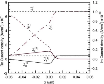
Fig. 5 (online colour at: www.pss-a.com) Real and imaginary part of ac amplitude of hole current density Jp displacement current density JD and total current density Jt.
3.4 Current density
In Fig. 5, the real and imaginary parts of the ac-hole current density and of the displacement current density are shown, the electron current contribution being negligible for this particular system. For the voltage situation V0 = 0, the imaginary part, i.e. the capacitive part of the total current, is the dominant contribution.
From the decrease of the hole current, one can see where the filling and emptying of the trap states takes place. The region between -0.05 µm and -0.01 µm corresponds to charging and emptying of the Et1 traps, whereas the
region from -0.01 µm to 0.01 µm corresponds to the Et2 states. 3.5 Electrical characteristics
From the as-obtained results, one produces the loss curve, i.e. G/ω as function of frequency and the capacitance-frequency-curve as given in Fig. 6. The C-f curve presents several steps, each corresponding to a mechanism where one element in the structure no longer responds to the applied voltage modulation. The remaining high-frequency value of 22 nF/cm2 corresponds to the dielectric capacitance. Any decrease in the C-f curve goes in parallel with a maximum of the G/ω curve. The peak at f = 0.25 Hz is due to the response of the Et2 states,
whereas the peak around 150 Hz is due to the Et1 states. The latter having a larger width of the density of states
function contribute with a larger peak in the G/ω curve. The last peak at 107Hz is due to the modulation of the hole concentration around the anode contact, which leads to a RsCd cut-off. Here Cd is the capacitance associated
with this charge modulation close to the anode contact, as illustrated by Fig. 2, and Rs is the series resistance of
the structure. No charge modulation occurs around the cathode, at least for the V0 = 0 case, therefore there is no
cut-off associated with this contact.
The ac curves depend strongly on the parameters used to describe the trap states. For organic compounds, their precise value is not known in any case. As one can see from the relations (12) and (19), the trap response depends essentially on the energy position Et relative to the valence or conduction band, the carrier thermal
velocity and the capture cross section. For σp, we have taken 10-15 cm2, but lower values down to 10-20 cm2 have been reported [25]. The value of 10 m/s for the thermal velocity corresponds to a material where a hopping mechanism leads to a rather efficient carrier conduction [26]. Band or ballistic transport would lead to a value of 107 cm/s, similar to that of a standard inorganic semiconductor, like silicon [22]. Taking an ionisation energy of the trap states of 0.7 eV instead of 0.5 eV produces at room temperature a shift of the defect cut-off frequency of the order of 3 decades. Admittance curves at different temperatures should give an additional information on the physical parameters, even if the thermal velocity and the capture cross section will be associated as a product. Therefore, we show in Fig. 7, the G/ω curves for 5 different temperatures. The structure around 107Hz is not reproduced, as its position only slightly changes when the hole mobility µp is constant. With a
temperature-dependent hole mobility, the position of this peak would scale with µp. With decreasing temperature, both
defect-related peaks move to lower frequencies. Deducing directly ionisation energies from Arrhenius plots requires some care, even in the case of discrete levels [27]. In the example treated here, the Arrhenius plot yields an activation energy of 0.49 eV for the lowest peak, and a value of 0.26 eV for the highest peak. The values are close, but not identical to the mean energies of the gaussian density of states functions E2 and E1. The difference
being due to the broadening of the defect states and to the fact that the frequency ωA, as given by relation (19) is
not strictly equal to the hole emission rate ep.
The Cole-Cole diagrams given in Fig. 8 illustrate the effect of the applied steady-state voltage V0 on the
ac-response of the structure. Whereas the plot of G/ω as function of C is a nearly perfect circle for the RsCd part of
the response, there is an enlargement of the circle for the Et2 contribution, which is even more pronounced for
the Et1 contribution. This reflects the effect of the width of the gaussian density of states function. Discrete levels
would have led to perfect circles in the latter case. This type of diagram may give a hint for establishing
equivalent electrical circuits, but in the case of a continuous distribution of trap states, this would require a series of distributed elements, with an increasing number of parameters corresponding to the various elements.
Interpretation of experimentally obtained electrical characteristics is a delicate task as this spectroscopic technique yields a global response. Features can be interpreted as being due to different layers of various compositions [1] or to a temperature dependence of the conductivity with a given activation energy [13]. An alternative way to explain the observed results would be to attribute them to trap states with a certain density of states function. Impedance spectroscopy measurements on different PPV derivatives [13] show loss curves with a three-peak structure similar to those given in Figs. 6 and 7. The lowest peak is at very low frequency, at about 10 2 Hz. An intermediate peak around 103 Hz at room temperature moves to lower frequencies with decreasing temperature, with activation energies in the range 0.40 eV to 0.46 eV. A higher structure above 106Hz could be due
to a RC cut-off implying a series resistance effect. Status: Postprint (Author’s version)
Fig. 6 Loss function G/ω and capacitance C as function of frequency for structure defined in Fig. 1 at steady-state voltage V0 = 0 V and temperature T=300K.
Fig. 7 Loss function G/ω as function of frequency for temperatures T = 320 K, 300 K, 280 K, 260 K and 240 K.
Fig. 8 Cole-Cole diagram for temperature T = 300 K and steady-state applied voltages V0 = -0.4 V, 0 V, 0.2 V and 0.4 V. Frequency is increasing from right to left.
3.6 Effect of contacts and trap DOS functions
Once the formalism established, it is easy to study numerically the physical implications of the presence of traps on the electrical characteristics. Modifying the parameters in a given value range, allows to see whether or not this may lead to an quantitative modification of the electrical characteristics.
First to get an observable feature like a peak in the loss curve or a step in the capacitance-frequency response, it is necessary that the defect-related cut-off frequency falls within the accessible range of standard admittance-meters, which is typically from 10-2Hz to several MHz. The order of magnitude of the trap characteristic frequencies is typically given by the electron or hole thermal emission rates, as given by Eqs. (11) and (12). At room temperature, the effective valence band or conduction band density of states is typically 1021 cm-3. Taking the degeneracy factor equal to 1, the remaining critical parameters are the trap energy and the capture
coefficients cp or cn. A defect located for example 0.5 eV from the valence or conduction band edge requires values of cn, cp between 10-14 and 10-6 s 1 to lead to an observable feature. The capture coefficients appear as products of the capture cross sections σn or σp and the respective thermal velocities vth. For organic
semiconductors, these parameters are not very well determined. Capture cross sections appear in the literature with values between 10-14 to 10-20 cm2. Taking the upper value, the thermal velocity should be greater than 1 cm/ s. With the lower value a thermal velocity of 106 cm/s is necessary. As a consequence, defects will not be observable in any case.
Fig. 9 (online colour at: www.pss-a.com) Capacitance-frequency curves for T =300 K, steady-state applied voltage V0 = 0V, with various combinations of left-hand hole injection barrier height qΦBL and right-hand electron injection barrier height qΦBR, with (qΦBL, qΦBR) = (0.2 eV, 0.6 eV) curve (a); (0.2 eV, 0.9 eV) curve (b); (0.2 eV, 0.3 eV) curve (c) and (0.05 eV, 0.6 eV) curve (d).
In Fig. 9, we show the capacitance-frequency curves for four different combinations of the left-hand and right-hand metallic contacts, with the double gaussian DOS distribution and V0 = 0 V, all other parameters identical to
those used along the paper. Curve (a) corresponds to the combination qΦBL = 0.2 eV and qΦBR = 0.6 eV, where qΦBL denotes the hole injection barrier at the left contact and qΦBR the electron injection barrier at the right
contact. In curves (b) and (c) the left barrier is kept equal to 0.2 eV, whereas the right-hand barrier is set equal to respectively 0.9 eV and 0.3 eV. In curve (d) we have taken qΦBL = 0.05 eV and qΦBR = 0.6 eV. Modifying the
values of the barrier-heights does of course not shift the position of the cut-off frequencies and the peaks in the loss-curve. The figure allows to illustrate two aspects inherent in the effect of a modification of the contact characteristic parameters on the resulting small-signal response. When comparing curves (a), (b) and (c) the capacitance in the frequency-range before any of the two cut-off frequencies is strongest for case (b), followed by case (a) and finally (c). This corresponds to the classification according to the total variation of the band edges or the defect bands over the width of the structure of respectively 1.3 eV, 1.6 eV and 1.9 eV. At zero applied voltage the hole Fermi-level is constant throughout the device, the three configurations correspond to an increasing angle between the Fermi-level and the defect states in the intersection region, i.e. where the
occupation of the states is modified when an ac-voltage is applied. The smaller the angle, the larger the width of band of states which are filled and emptied and the larger the resulting contribution of the trap states to the capacitance. A similar effect could be produced through modification of the distance between the two etallic contacts. These conclusions hold as long as a modification of one of the barrier heights only leads to a uniform bending of the band diagram. The parameter set used for case (d) leads to a total variation of the band edges of 1.75 eV. One would therefore expect a resulting capacitance curve at midway between curves (a) and (b). The curve (d) shown in the Fig. 9, is however very close to curve (a). This can only be understood with a detailed Status: Postprint (Author’s version)
analysis of the band diagram which for this case yields a bending close to the left contact, nearly equal to the modification of the hole injection barrier and a nearly unmodified structure for x values larger than -0.04 µm. The effect of the variation of the parameter set will be illustrated on two cases.
In Fig. 10 we show the effect of the shape of the density of states function Dt. We have analysed four different
cases corresponding to a discrete trap, a gaussian distribution, a rectangular shape and an exponential DOS function, all having the same total trap concentration of 5 × 1016 cm 3. The discrete trap is located 0.3 eV above the valence band edge, the single gaussian distribution has the same mean value of 0.3 eV above Ev and a
standard deviation of 0.05 eV. The distribution of rectangular shape is centred at 0.3 eV above Ev and has a total
width of 0.3 eV, the exponential distribution has a exp (-(Et-Ev)/Eλ) dependence, with Eλ = 0.3 eV. The resulting peak in the G/ω curve is strongest with the smallest width for the case of the discrete trap state, as expected. The gaussian peak is still centred around the mean frequency value, whereas the response of the rectangular
distribution shifts to lower frequencies, a consequence of the fact that the displacement of the Fermi level due to the applied voltage does not cover the whole defect band. The exponential DOS leads to a structureless, nearly constant contribution to the G/ω function.
Fig. 10 (online colour at: www.pss-a.com) G/ω as function of frequency for discrete trap state at 0.3 eV above the valence band edge Ev (curve a), Gaussian distribution with mean value of 0.3 eV above Ev and standard deviation σE = 0.05 eV (curve b), DOS function with rectangular shape centered at 0.3 eV above Ev and width of 0.3 eV (curve c), and exponential distribution with decay length Eλ = 0.3 eV. Integrated defect concentration is Nt = 5 × 1016 cm 3 in all cases.
4 CONCLUSION
We have presented the small-signal analysis of an organic diode with a continuous distribution of trap states. Numerical application has been made to a hole conducting layer with a trap density of states composed of two gaussian functions. It illustrates the various steps leading from the applied modulating voltage to the
macroscopic electrical characteristics. The formalism can of course be used to study more complex systems, such as structures consisting of several layers of organic semiconductors, or traps with a space-dependent concentration, as is the case for interface traps. The microscopic parameters can be extended to any density of states function, with energy-dependent parameters like capture cross sections, or trap depending carrier
mobilities. These developments may help in the interpretation of the electrical characteristics of organic diodes, complementing the analysis by equivalent electrical circuits. It constitutes an approach giving access to microscopic information on the trap states, leading finally to a better understanding of the mechanisms governing the light emission efficiency of organic light emitting structures.
REFERENCES
[1] W. Brütting, S. Berleb, and A. G. Mückl, Org. Electron. 2, 1 (2001). [2] A. J. Campbell, D. D. C. Bradley, and D. G. Lidzey, Opt. Mat. 9, 114 (1998).
[3] A. J. Campbell, D. D. C. Bradley, E. Werner, and W. Briitting, Org. Electron. 1, 21 (2000). [4] A. J. Campbell, D. D. C. Bradley, E. Werner, and W. Briitting, Synth. Met. 111/112, 273 (2000). [5] S. Berleb, A. G. Miickl, W. Briitting, and M. Schwoerer, Synth. Met. 111/112, 341 (2000). [6] N. Von Malm, R. Schmechel, and H. Von Seggern, Synth. Met. 126, 87 (2002).
[7] J. Steiger, R. Schmechel, and H. Von Seggern, Synth. Met. 129, 1 (2002).
[8] F. T. Reis, D. Mencaraglia, S. Oould Saad, I. Séguy, M. Oukachmih, P. Jolinat, and P. Destrael, Synth. Met. 138, 33 (2003). [9] D. M. Taylor and H. L. Gomes, J. Phys. D: Appl. Phys. 28, 2554 (1995).
[10] M. G Harrison, J. Griiner, and G. C. W. Spencer, Synth. Met. 76, 7 (1996).
[11] J. Scherbel, P. H. Nguyen, G. Paasch, W. Briitting, and M. Schwoerer, J. Appl. Phys. 83, 5045 (1998).
[12] S. H. Kim, K. H. Choi, H. M. Lee, D. H. Hwang, L. M. Do, H. Y. Chu, and T. Zyung, J. Appl. Phys. 87, 882 (2000). [13] S. Forero-Lenger, J. Gmeiner, W. Briitting, and M. Schwoerer, Synth. Met. 111/112, 165 (2000).
[14] J. Drechsel, M. Pfeiffer, X. Zhou, A. Nollau, and K. Leo, Synth. Met. 127, 201 (2002). [15] Y. S. Lee, J.-H. Park, J. S. Choi, and J. I. Han, Jpn. J. Appl. Phys. 42, 2715 (2003).
[16] S. H. Kim, J. W. Jang, K. W. Lee, C. E. Lee, and S. W. Kim, Solid State Commun. 128, 143 (2003). [17] I. H. Campbell, D. L. Smith, and J. P. Ferraris, Appl. Phys. Lett. 66, 3030 (1995).
[18] H. L. Gomes, P. Stallinga, H. Rost, A. B. Holmes, M. G. Harrison, and R. H. Friend, Appl. Phys. Lett. 74, 1144 (1999). [19] S. Selberherr, Analysis and Simulation of Semiconductor Devices (Wiley, New York, 1981).
[20] M. Sakhaf and M. Schmeits, J. Appl. Phys. 80, 6839 (1996). [21] C. D. J. Blades and A. B. Walker, Synth. Met. 111/112, 335 (2000). [22] G. Paasch and S. Scheinert, Synth. Met. 122, 145 (2001).
[23] P. H. Nguyen, S. Scheinert, S. Berleb, W. Brütting, and G. Paasch, Org. Electron. 2, 105 (2001). [24] A. Nesterov, G. Paasch, S. Scheinert, and T. Lindner, Synth. Met. 130, 165 (2002).
[25] O. Gaudin, R. B. Jackman, T. P. Nguyen, and P. Le Rendu, J. Appl. Phys. 90, 4196 (2001). [26] G. Paasch, T. Lindner, and S. Scheinert, Synth. Met. 132, 97 (2002).
[27] M. Schmeits, N. D. Nguyen, and M. Germain, J. Appl. Phys. 89, 1890 (2001).